Photonic Matrix Computing
1. Foundations of Neural Multiplication and Matrix Operations
1.1 Neural Network Computation as Matrix Multiplication
Neural networks compute outputs by repeatedly applying linear transforms and then nonlinearity. The linear part is matrix multiplication; the nonlinearity is what makes the whole system more than a fancy calculator. A clean way to see this is to start with one layer and then generalize.
From Neurons to Vectors
Consider a layer with input vector \(x\in\mathbb{R}^{n}\) and \(m\) outputs. Each output neuron forms a weighted sum of inputs plus a bias:
\[ y_i = \sum_{j=1}^{n} W_{ij} x_j + b_i \]
Stacking all \(y_i\) into a vector \(y\in\mathbb{R}^{m}\) gives the compact form:
\[ y = W x + b \]
This is the first key best practice: keep the shapes explicit. If \(W\) is \(m\times n\), then \(x\) must be length \(n\), and \(y\) becomes length \(m\). When shapes match, the math stops being mysterious and starts being mechanical.
Batch Computation as Matrix Multiplication
Training and inference usually process many examples at once. Put \(B\) input vectors into a matrix \(X\in\mathbb{R}^{n\times B}\) (columns are examples). Then the layer output is:
\[ Y = W X + b\mathbf{1}^T \]
Here \(b\in\mathbb{R}^{m}\) is broadcast across the batch using a ones vector \(\mathbf{1}\in\mathbb{R}^{B}\). This broadcasting detail matters for implementation because it determines whether you add bias per column or per row.
Nonlinearity as a Separate Step
After the linear transform, a nonlinearity \(\phi\) is applied elementwise:
\[ Z = \phi(Y) \]
Elementwise means \(Z_{ij}=\phi(Y_{ij})\). This separation is useful because it lets hardware focus on the matrix multiply part, while the nonlinearity can be approximated or handled in a different stage.
A Concrete Example with Shapes
Let \(x\in\mathbb{R}^3\), and we want \(y\in\mathbb{R}^2\). Choose:
\[ W = \begin{bmatrix} 1 & -1 & 2 \\ 0 & 3 & 1 \end{bmatrix},\quad b=\begin{bmatrix} 0.5 \\ -1 \end{bmatrix} \]
For a single input \(x=[2,1,-1]^T\):
\[ Wx = \begin{bmatrix}1\cdot2 + (-1)\cdot1 + 2\cdot(-1) \\ 0\cdot2 + 3\cdot1 + 1\cdot(-1)\end{bmatrix} =\begin{bmatrix}-1 \\ 2\end{bmatrix} \]
Then \(y=Wx+b=[-0.5,,1]^T\). The arithmetic is straightforward; the important part is that every neuron output is one row of \(W\) dotted with \(x\).
Mind Map: Matrix Multiplication View of Neural Layers
Data Layout Choices That Affect Correctness
Whether you store examples as rows or columns changes how you write the multiplication. If you store \(X\) as \(B\times n\) (rows are examples), then the same layer is:
\[ Y = X W^T + b \]
Both are correct; the best practice is to pick one convention and stick to it across the codebase and experiments. A common bug is mixing conventions so that you accidentally compute \(W^T x\) instead of \(W x\).
Why This Matters for Photonic Matrix Computing
Photonic accelerators typically implement linear transforms efficiently, because interference naturally performs weighted sums. Once you express a layer as \(Y=W X + b\mathbf{1}^T\), you can identify what must be implemented optically (the \(W X\) part) and what can be handled separately (bias addition and nonlinearities). Even before discussing hardware, this decomposition keeps the system design grounded in the same matrix math used in standard neural network training.
Quick Reference Summary
- One layer linear part: \(y=W x + b\)
- Batch linear part: \(Y=W X + b\mathbf{1}^T\)
- Activation: \(Z=\phi(Y)\) elementwise
- Best practice: track shapes and broadcasting rules every time you write the equation.
1.2 Dataflow Choices for Multiply Accumulate Workloads
Multiply-accumulate (MAC) is the core rhythm of neural layers: for each output neuron, you sum products of inputs and weights. In photonic matrix computing, the “product” can happen optically, but the “sum” still depends on how you route signals, schedule measurements, and reuse data. Dataflow choices decide whether you pay energy in optical power, detector readout, control overhead, or memory movement.
Start with the Baseline: What Must Be Scheduled
A typical dense layer computes Y = XW + b. For a batch, you compute multiple rows of Y. The hardware must decide:
- Which dimension is mapped to parallel optical channels (often columns of W or rows of X).
- Which dimension is mapped to time multiplexing (often tiles of W or segments of X).
- How intermediate results are accumulated across tiles and batches.
A useful mental model is to treat each MAC as belonging to a coordinate triple (batch index n, output index m, input index k). Dataflow is the rule for grouping many k terms into one optical operation, then combining groups into the final sum for each (n, m).
Mind Map: Dataflow Knobs and Their Consequences
Three Practical Dataflows and When They Win
1) Output-Stationary Accumulation
You keep partial sums for each output neuron close to where they are accumulated. In practice, you stream input tiles and reuse the same output accumulation buffers.
- Best when: output dimension is modest, and you want to minimize repeated writes of partial sums.
- Photonic implication: you may measure multiple optical contributions and immediately add them digitally into the same output buffer.
Example: Suppose W is 1024×1024 and you tile k into blocks of 64. For each output m, you run 16 optical measurements (one per k tile) and accumulate into Y[n, m]. You reuse the output buffer across all k tiles, so you avoid storing all partial sums for every tile.
2) Weight-Stationary Transform Reuse
You treat the photonic mesh as a reusable transform for a fixed weight matrix tile. Inputs are streamed through while weights stay put.
- Best when: weights are constant for long stretches, such as inference on a fixed model.
- Photonic implication: calibration and phase alignment are amortized because the same mesh settings apply across many batches.
Example: For inference with batch size 128, you set the mesh once for a W tile. Then you feed 128 different X tiles, measuring outputs each time. The dataflow reduces reconfiguration events, which often dominate control energy and settling overhead.
3) Input-Stationary Streaming with Tiled Weights
You hold an input tile in a local buffer and apply multiple weight tiles to it.
- Best when: input reuse is high, such as convolution lowered to matrix form where the same patch contributes to many outputs.
- Photonic implication: you may reduce peak optical power by scaling inputs per tile, but you must manage more partial sums across weight tiles.
Example: If you lower a convolution to a GEMM, each input patch contributes to many output channels. You keep that patch’s representation stable, apply weight tiles for different output-channel groups, and accumulate results for the corresponding output channels.
Accumulation Placement: Optical vs Electronic
Optical interference can compute linear combinations efficiently, but accumulation across tiles is where errors can stack up.
- Electronic accumulation is usually straightforward: you store partial sums in higher precision and apply scaling consistently.
- Optical accumulation can reduce digital adds, but it requires careful control of phase drift and detector dynamic range.
A practical rule: if your partial sums span many tiles, prefer electronic accumulation unless your noise and dynamic range budget is explicitly verified.
A Concrete Scheduling Example with Tiling
Consider computing Y for one batch element with W split into k tiles: W = [W0, W1, …, W15], each Wi has width 64. For each output tile of m:
- Encode Xk tile (the corresponding 64 inputs).
- Apply the photonic transform for Wi.
- Detect the resulting contribution.
- Add it into the output buffer for that (n, m) tile.
This is output-stationary in the accumulation dimension and weight-stationary in the transform dimension for each Wi.
Best Practices That Follow from the Dataflow
- Keep scaling consistent across tiles so that partial sums are comparable when added.
- Minimize reconfiguration events by grouping operations that share the same mesh settings.
- Choose tile sizes that fit detector dynamic range; if saturation happens, the dataflow choice becomes a numerical problem.
- Buffer only what you must: store final outputs and accumulate partial sums immediately when possible.
Dataflow is not a separate concern from photonic computation; it is the mechanism that decides where energy and error budgets are spent. Once you pick which dimension is parallel and which is tiled, the rest of the design becomes a bookkeeping exercise with measurable consequences.
1.3 Numerical Formats for Neural Weights and Activations
Neural matrix multiplication is only as good as the numbers you feed it. In photonic matrix computing, the format of weights and activations determines how accurately optical interference represents the intended linear transform, and how much headroom you need to avoid saturating detectors or losing small signals in noise.
What “Format” Means in Practice
A numerical format has three practical parts: (1) value range, (2) precision, and (3) representation of sign. For example, a weight matrix element might be stored as an integer with a scale factor, or as a floating-point number with many bits. In optical implementations, you also care about how that representation maps to optical amplitude and phase, and how the detector converts optical intensity back into numbers.
A useful mental model is: the same mathematical matrix can be implemented with different formats, but each format changes the error you introduce at encoding, during propagation, and at detection.
Range First, Precision Second
Start with range because it sets the operating point. If activations are too large, optical power may clip at the modulator or saturate the photodetector. If activations are too small, shot noise and readout noise dominate.
A simple best practice is to normalize activations per layer so their typical magnitude fits a target interval. For instance, if you expect activations to mostly lie in −1 to 1, you can choose a scale so that the optical encoding uses most of the available dynamic range without frequently hitting the extremes.
Precision then controls how finely you represent values within that range. In quantized systems, precision is often the number of discrete steps. If you quantize a value x in −1..1 to 8-bit signed integers, you get 256 steps across the range (including sign), which means the smallest representable change is about 2/255 ≈ 0.0078. That step size becomes a direct contributor to multiplication error.
Sign Handling Without Confusion
Optical intensity is nonnegative, so sign must be represented indirectly. Common strategies include:
- Signed weights via differential encoding: represent a signed value as the difference between two nonnegative channels. Example: store w as (w+ , w−) where w = w+ − w− and both are nonnegative. If w = -0.25, you might set w+ = 0 and w− = 0.25.
- Signed weights via phase encoding: represent sign through phase (e.g., 0 vs π). Example: a positive weight uses constructive interference, while a negative weight flips the phase so the contribution subtracts.
Differential encoding is often easier to reason about because it keeps magnitudes nonnegative, but it doubles the number of channels to detect. Phase encoding can be more compact, but it is sensitive to phase errors.
Quantization Levels and Their Error Shape
Quantization error is not just “more noise”; it has structure. If you quantize uniformly, the error for each value is roughly bounded by half a step. For multiplication, the error in the product depends on both the quantization step and the magnitude of the other operand.
Concrete example: suppose activations a are quantized with step size Δa ≈ 0.01, and weights w are quantized with step size Δw ≈ 0.02. If a and w are around 0.5 in magnitude, then a perturbation of ≈±0.005 in a changes the product by about 0.5×0.005 = 0.0025, while a perturbation of ≈±0.01 in w changes it by about 0.5×0.01 = 0.005. The larger step dominates.
This is why many systems choose different bit widths for weights and activations: the one with the larger effective step size usually contributes more to the final error.
Fixed-Point Formats for Optical Mapping
Fixed-point formats are popular because they make scaling explicit. A typical scheme stores an integer q and interprets the real value as x = q / S, where S is a scale.
Example: choose S = 128 for activations so that a value a = 0.5 becomes q = round(0.5×128) = 64. Then a = q/S = 64/128 = 0.5 exactly. If a = 0.503, q = round(0.503×128) = 65, so the represented value is 65/128 = 0.5078. That difference is the quantization error.
In photonic settings, the scale S is also your bridge between numeric magnitude and optical amplitude or phase settings. A good best practice is to pick S so that the encoded values rarely exceed the representable range, because clipping creates large, nonlocal errors.
Floating-Point Formats and Why They Still Matter
Floating-point formats can reduce quantization error by allocating more precision where values are small. However, they complicate hardware mapping because you still need a consistent encoding for the optical device. Even if the model stores weights in floating point, you often quantize them at the interface.
A practical workflow is: keep training in higher precision, then quantize to a fixed format for the photonic execution path. That way, the photonic format is consistent and calibration-friendly.
Mind Map: Numerical Formats for Neural Weights and Activations
Worked Example: Choosing a Format for One Layer
Assume a layer expects activations mostly in −1..1 and weights mostly in −0.5..0.5.
- Pick range targets: set activation scale so that ±1 maps near the maximum representable magnitude without frequent clipping. If you use signed 8-bit integers for activations, the maximum integer is 127, so choose S a so that 1 ≈ 127/Sa, giving Sa ≈ 127.
- Pick weight scale: for weights in −0.5..0.5, choose a weight scale Sw so that 0.5 maps near 127. That gives Sw ≈ 254.
- Quantize with rounding: represent a = 0.73 as q = round(0.73×127) = 93, so ã = 93/127 = 0.7323. Represent w = -0.21 as q = round(-0.21×254) = -53, so w̃ = -53/254 = -0.2087.
- Estimate error impact: the activation step is about 1/127 ≈ 0.0079; the weight step is about 1/254 ≈ 0.0039. Since the activation step is larger, activation quantization likely dominates product error.
This example shows the core discipline: choose scales to avoid clipping, then choose precision where it matters most for the multiplication error budget.
1.4 Energy Cost Drivers in Conventional Digital Multiply Accumulate
Conventional neural inference spends most of its energy in moving numbers around and in repeatedly performing the same arithmetic pattern. A multiply-accumulate (MAC) is simple on paper, but in hardware it triggers a chain of events: fetch operands, align them, multiply, add, and then write results back. Each step has a different energy cost, and the dominant one depends on where the data lives.
Where the Energy Goes in a MAC
A useful mental model is to split a MAC into three buckets: compute, memory traffic, and control overhead. Compute energy covers the switching activity inside multipliers and adders. Memory traffic energy covers reading activations and weights, plus writing partial sums. Control overhead covers clocking, buffering, and address generation that keep the pipeline fed.
A practical rule: if your design can reuse data already in registers or SRAM, energy drops sharply. If it must stream from DRAM for every MAC, energy rises fast because DRAM access is expensive.
Memory Traffic Dominates When Reuse Is Poor
Consider a fully connected layer with input vector length K and output length N. A straightforward implementation computes N×K MACs. If weights are stored in DRAM and fetched for each output neuron, you repeatedly pay the cost of weight movement. Better dataflows keep weights stationary or keep activations stationary so that each fetched value participates in many MACs.
Example: Suppose each weight is 8 bits and each activation is 8 bits. If you process one output neuron at a time, you may stream the entire input vector K for each neuron, causing K reads per neuron. If instead you tile the computation so that a block of activations is loaded once and reused across multiple neurons, the number of activation reads per MAC decreases.
Compute Energy Depends on Precision and Implementation
Digital multipliers scale with bit-width. Going from 8-bit to 16-bit typically increases switching activity and area, which increases energy per operation. Even when the arithmetic is “the same” conceptually, the circuit complexity changes.
Example: In an 8-bit MAC, the multiplier can use smaller partial-product arrays. In a 16-bit MAC, there are more partial products and more carry propagation in the adder stage. The energy per MAC rises even if memory traffic stays constant.
Compute energy also depends on whether you use dense arithmetic or exploit sparsity. If many weights are zero and the hardware skips multiplications, compute energy can drop. However, skipping only helps if the system also avoids fetching or processing the corresponding operands.
Accumulation and Partial Sums Create Extra Writes
Accumulation is not free. Partial sums must be stored somewhere while the pipeline processes the next chunk of K. If the accumulator spills to memory, you pay extra reads and writes.
Example: For K=1024, you might process K in chunks of 16. After each chunk, you update a running sum. If the running sum stays in a register file or on-chip SRAM, the update is cheap. If it must be written to off-chip memory between chunks, energy balloons.
Control Overhead and Pipeline Inefficiency Matter
Even with the same arithmetic, real systems waste energy when the pipeline stalls. Stalls can come from cache misses, irregular memory access patterns, or synchronization between compute and DMA engines.
Example: If your tiling strategy causes non-contiguous reads, you may lose cache locality. The compute unit waits, but the memory system still consumes energy for transfers and buffering. The result is lower MAC throughput and higher energy per useful MAC.
Mind Map: Energy Cost Drivers
A Concrete Mini-Example with Numbers
Assume a simplified scenario where energy per access differs by orders of magnitude: on-chip SRAM read is “cheap,” DRAM read is “expensive.” If a design performs one DRAM read per MAC, energy is dominated by memory traffic. If tiling reduces DRAM reads so that each weight is fetched once and reused across many MACs, the same MAC arithmetic suddenly becomes the smaller part of the budget.
This is why energy optimization often starts with data movement and reuse, not with changing the multiply itself. The arithmetic is the headline, but the energy bill is mostly the supporting cast.
1.5 Mapping Matrix Shapes to Hardware Execution Patterns
Matrix multiplication is the same math everywhere, but the hardware “shape” of the computation changes the story. In photonic matrix computing, you typically realize a linear transform using an optical mesh, then detect outputs. So mapping a matrix’s dimensions to an execution pattern means choosing how you partition rows and columns, how you reuse the same optical hardware, and how you align input encoding with detector outputs.
Step 1: Start with the Matrix Shape and the Hardware Primitive
Assume your target is a weight matrix \(W\in\mathbb{R}^{M\times N}\) and you want \(Y=W X\) where \(X\in\mathbb{R}^{N\times B}\) for batch size \(B\). Photonic meshes usually implement a transform from an input vector of length \(N\) to an output vector of length \(M\). That gives a natural “primitive” mapping: one optical run computes one \(M\times N\) multiply for one batch column.
Best practice: write down three numbers before designing anything—\(M\), \(N\), and the mesh I/O sizes \(M_{hw}\), \(N_{hw}\). If \(M\neq M_{hw}\) or \(N\neq N_{hw}\), you will tile.
Step 2: Choose a Tiling Direction That Matches Reuse
If the mesh can handle \(N_{hw}\) inputs at once, but your \(N\) is larger, split columns of \(W\) into blocks of width \(N_{hw}\):
- \(W=[W_0;W_1;\dots]\) where each \(W_k\in\mathbb{R}^{M\times N_{hw}}\)
- Then \(Y=\sum_k W_k X_k\) where \(X_k\) is the corresponding slice of \(X\)
If instead \(M\) is larger than \(M_{hw}\), split rows and accumulate outputs. Column-tiling often wins when input activations can be reused across multiple output blocks; row-tiling often wins when weight blocks can be streamed efficiently.
Concrete example: Suppose \(W\) is \(256\times 1024\) and your mesh is \(256\times 256\). You can compute \(Y\) with 4 column tiles because \(1024/256=4\). Each tile produces a full 256-length output, and you sum them elementwise.
Step 3: Map Batch Size to Execution Scheduling
Batch size \(B\) affects how many times you run the mesh. If you encode one batch column per optical run, total runs scale with \(B\). If your encoding supports multiple batch items in parallel (for instance, using different wavelengths or time slots), you can reduce runs, but you must ensure the detection model separates them cleanly.
Best practice: keep the detection model explicit. If your detector outputs are linear combinations of optical fields, then “parallel batch” only works when the separation is orthogonal in the measurement space.
Step 4: Handle Non-Square Matrices Without Losing Structure
Many neural layers produce rectangular matrices. A common pitfall is forcing everything into square blocks and then discarding the remainder. Instead, use partial tiles:
- For the last column tile, use only \(N\bmod N_{hw}\) inputs and pad the rest with zeros.
- For the last row tile, detect only the needed outputs and ignore the rest.
Example: \(W\in\mathbb{R}^{300\times 512}\) with mesh \(M_{hw}=256\), \(N_{hw}=256\). You need two row tiles (256 + 44) and two column tiles (256 + 0). That yields 2×2=4 mesh runs, with padding on the final row tile.
Step 5: Align Accumulation with the Optical-To-Electrical Interface
Tiling introduces sums across tiles. In photonic systems, the optical transform is linear, but accumulation can happen either:
- In the electrical domain after detection (sum detected outputs), or
- In the optical domain before detection (harder, requires careful power/phase handling).
Best practice: prefer electrical accumulation because it keeps the optical part purely linear and avoids mixing terms that should remain separable.
Step 6: Use a Mind Map to Keep the Mapping Decisions Straight
Mind Map: Mapping Matrix Shapes to Hardware Execution Patterns
Step 7: A Compact Worked Mapping Recipe
For \(W\in\mathbb{R}^{M\times N}\), mesh \(M_{hw}\times N_{hw}\), and batch \(B\):
- Compute \(T_r=\lceil M/M_{hw}\rceil\), \(T_c=\lceil N/N_{hw}\rceil\).
- For each row tile \(r\) and column tile \(c\), run the mesh on the corresponding \(N_{hw}\)-length input slice (with zero padding if needed).
- Detect outputs for the \(M_{hw}\) rows of that tile, then place them into the correct segment of \(Y\).
- If you used column tiling, accumulate \(Y\) across \(c\) by summing the partial results elementwise.
- Repeat for each batch column (or for each separated batch slot if your encoding supports it).
This recipe keeps the math consistent with the hardware’s I/O limits, and it prevents the classic “the indices look right but the accumulation is in the wrong place” bug.
2. Optical Interference and Coherent Light as a Computing Medium
2.1 Coherence, Phase, and Interference Fundamentals
Photonic matrix computing relies on a simple idea: when fields add, the result depends on their relative phase, not just their power. Coherence tells you whether that phase relationship stays usable long enough for computation; interference tells you how the fields combine into intensities that detectors can measure.
Coherence: When Phase Stays Meaningful
Start with a monochromatic field at angular frequency \(\omega\): \[E(t)=E_0 e^{j(\omega t+\phi)}\] The phase \(\phi\) is the knob that interference uses. Coherence describes how stable the phase difference between two paths remains over time and across the device.
Two practical coherence notions matter:
- Temporal coherence: how long the phase stays correlated. If path length difference \(\Delta L\) exceeds \(c,\tau_c\) (with \(\tau_c\) the coherence time), interference visibility collapses.
- Spatial coherence: how well different points across the beam share phase. Poor spatial coherence averages interference fringes out.
Easy example: Send light through two arms with a fixed delay. If the delay is small compared to the coherence time, you see stable fringes. If you increase the delay beyond that, the detector output becomes roughly the sum of intensities with no reliable interference pattern.
Phase: The Quantity Optical Hardware Actually Controls
In waveguide meshes, phase shifters change the phase accumulated along a path. A phase shift \(\theta\) multiplies the complex field by \(e^{j\theta}\). Because matrix multiplication is linear in complex amplitudes, phase control is the mechanism that makes programmable linear transforms possible.
Easy example: Suppose two inputs produce fields \(A\) and \(B\) at a combiner. If one path applies phase \(\theta\), the output field is \(A + B e^{j\theta}\). The detected intensity is \[I(\theta)=|A|^2+|B|^2+2,\Re{A B^* e^{j\theta}}\] The last term is the interference term; it oscillates with \(\theta\).
Interference: From Complex Fields to Measurable Intensity
Interference is easiest to reason about using complex amplitudes. Consider two equal-magnitude fields \(A=B=E\) with relative phase \(\theta\): \[I(\theta)=2|E|^2(1+\cos\theta)\]
- If \(\theta=0\), then \(I=4|E|^2\) (constructive interference).
- If \(\theta=\pi\), then \(I=0\) (destructive interference).
This is why phase errors matter. If the intended phase is \(\pi\) but the actual phase is \(\pi+\epsilon\), then \(\cos(\pi+\epsilon)=-\cos\epsilon\approx-(1-\epsilon^2/2)\), so the “zero” becomes a small but nonzero intensity proportional to \(\epsilon^2\).
Visibility: The Practical Measure of Interference Quality
Real systems have loss, polarization mismatch, and finite coherence. A common way to summarize interference quality is visibility \(V\), defined so that \[I(\theta)=I_\text{avg}\bigl(1+V\cos\theta\bigr)\]
- \(V=1\) means perfect contrast.
- \(V=0\) means no usable interference term.
Easy example: If one arm has extra loss, the interference term scales down relative to the average. Even with perfect phase control, unequal amplitudes reduce the maximum achievable contrast.
Mind Map: Coherence, Phase, and Interference
Worked Micro-Example for Intuition
Imagine a 2×2 interference element that combines two path contributions into one detector. Let \(A=1\) and \(B=0.8\). If the phase is set to \(\theta=\pi\), the ideal output intensity would be \[I=|1-0.8|^2=0.04\] Now include a phase error \(\epsilon=0.1\) rad so \(\theta=\pi+\epsilon\). The output becomes \(I=|1-0.8e^{j\epsilon}|^2\), which evaluates to a noticeably larger value than 0.04. This single calculation shows the chain: coherence must preserve phase, phase control must be accurate, and interference converts those controlled phases into detector-relevant intensity changes.
2.2 Complex Field Representation for Computation
Optical interference computes with the complex electromagnetic field, not directly with intensity. To use wave optics for matrix multiplication, you represent each signal as a complex number whose magnitude controls how much light you have and whose phase controls how the light lines up with other paths.
From Real Values to Complex Fields
Start with a real-valued input vector \(x\). In a photonic linear transform, each output is a weighted sum of inputs, but the weights act on complex fields. A practical bridge is to encode \(x\) into either:
- Complex amplitude encoding: \(x_k \rightarrow E_k = a_k e^{j\phi_k}\), where \(a_k\) carries the value and \(\phi_k\) is chosen (often 0 or a controlled reference).
- Phase-only encoding: \(x_k\) is mapped to phase while amplitude is kept roughly constant, which can simplify some hardware but complicates value recovery.
A common baseline is amplitude encoding with a fixed phase reference: \(E_k = x_k\) (or a scaled version) and \(\phi_k = 0\). Then the optical network implements a complex linear map:
\[\mathbf{E}_{out} = \mathbf{H},\mathbf{E}_{in}\]
where \(\mathbf{H}\) is the transfer matrix realized by the waveguide mesh.
Why Complex Numbers Matter
Intensity is what detectors measure, but intensity is derived from the complex field:
\[I = |E|^2 = E E^*\]
If you only tracked intensity through the network, you would lose the sign and relative timing information that interference depends on. Two fields with equal intensity but different phase can produce very different interference outcomes after combining.
A quick example: let \(E_1 = 1\) and \(E_2 = 1\). If they add in-phase, \(E = 2\) and \(I = 4\). If they add out-of-phase, \(E = 0\) and \(I = 0\). The detector sees intensity, but the network’s behavior is governed by complex addition.
Mapping Matrix Multiplication to Optical Operations
In neural multiplication, you want \(y_i = \sum_k W_{ik} x_k\). In optics, you typically implement a complex-valued linear transform first, then convert to a real output.
A standard workflow is:
- Encode \(x_k\) into \(E_{in,k}\).
- Program the mesh so that \(E_{out,i} = \sum_k H_{ik} E_{in,k}\).
- Detect intensity or field-related quantities to produce \(y_i\).
To make step 3 match a linear neural layer, you choose an encoding and detection model that yields an approximately linear relationship over the operating range. For instance, if you use small-signal modulation around a bias field, the intensity change can be made proportional to the real part of the complex field sum.
Mind Map: Complex Field Representation
Example: In-Phase and Out-of-Phase Addition
Consider a 2-input combiner that produces \(E = E_1 + E_2\). Let both inputs have magnitude 1.
- Case A: \(E_1 = 1\), \(E_2 = 1\) so \(E=2\), \(I=4\).
- Case B: \(E_1 = 1\), \(E_2 = -1\) so \(E=0\), \(I=0\).
This is the core reason complex field representation is not optional. The network can implement subtraction through phase control, even though the detector never directly reads “negative light.”
Advanced Detail: Real Outputs from Complex Fields
Neural outputs are real numbers, but optical fields are complex. A common approach is to arrange the computation so that the detected quantity depends on a chosen component of the complex result.
One robust method is quadrature-style readout: split the optical output into two paths with a relative phase shift of \(\pi/2\), then combine the two measured intensities to estimate the real and imaginary parts. Even when you don’t implement full quadrature hardware, the conceptual model helps you reason about what the detector is actually extracting.
A simpler alternative is to restrict \(H\) and the encoding so that the relevant neural quantity aligns with the real part of \(E_{out}\) over the expected range. That constraint reduces flexibility but makes the mapping from complex computation to real-valued neural arithmetic more predictable.
Best Practices for Complex Representation
- Use a consistent phase reference across the encoding and the mesh programming, so that “phase 0” means the same physical thing for every input.
- Scale inputs to keep the detection model in its approximately linear regime, because intensity detection is inherently nonlinear in \(E\).
- Treat negative weights as phase-controlled interference, not as negative intensity. If you need \(-x\), you generally implement it by shifting phase so the contributions cancel rather than by trying to send negative light.
These practices keep the complex-field math aligned with what the hardware can reliably measure, turning interference from a mystery into a controlled arithmetic tool.
2.3 Intensity Detection and the Role of Photodetectors
Optical interference gives you a field pattern; neural matrix multiplication needs numbers. In most photonic matrix computing schemes, the optical field is converted into electrical signals by photodetectors, and those electrical signals represent the detected intensities. The key idea is simple: interference happens in the complex field, while most detectors respond to the squared magnitude of that field.
From Field to Intensity
Represent the optical output of one waveguide output port as a complex amplitude \(E\). The detector current is proportional to optical power, which is proportional to intensity \(I\propto |E|^2\). If the field is a sum of contributions from multiple inputs, \(E=\sum_k a_k\), then \(|E|^2 = \left|\sum_k a_k\right|^2 = \sum_k |a_k|^2 + \sum_{k\neq j} a_k a_j^*.\) The cross terms \(a_k a_j^*\) are the interference terms that carry the “mixing” needed for matrix multiplication. Best practice: design the encoding so that the desired matrix product appears in the interference cross terms, not only in the individual power terms.
What Photodetectors Actually Measure
A photodetector converts incident optical power into a current \(i\). A common model is \[ i = R,P + i_{\text{noise}}, \] where \(R\) is responsivity (A/W) and \(P\) is optical power at the detector. In a coherent interference setup, \(P\) is proportional to intensity at the output port, so the detector current is proportional to \(|E|^2\).
Practical nuance: many systems use balanced detection to reduce sensitivity to common-mode intensity fluctuations. In balanced detection, two detectors measure two complementary outputs, and the difference current cancels parts of the noise that are shared. Example: if a laser intensity drift adds the same offset to both outputs, subtracting them removes most of that offset, leaving the interference-dependent component.
Detector Bandwidth and Integration Window
Neural inference is often treated as a steady computation, but detectors have finite bandwidth. If the optical modulation or symbol timing is too fast for the detector, the measured current becomes a filtered version of the true intensity. Best practice: choose an integration window that matches the symbol period and the detector’s electrical response time.
Example: suppose each input vector is held constant for \(T\) seconds. If the detector’s effective time constant is much smaller than \(T\), the detector current tracks intensity accurately. If it is comparable to \(T\), the output averages over transitions, effectively mixing adjacent symbols and corrupting the matrix result.
Noise Sources and Their Effect on Matrix Accuracy
Detector noise matters because matrix multiplication amplifies small errors across many outputs. Common contributors include shot noise (from the discrete nature of photons), thermal noise (from electronics), and relative intensity noise (from the laser).
Shot noise scales with the detected optical power: higher power reduces relative shot noise but increases power-related loss and potentially heating. Best practice: operate at a power level where shot noise is not dominant, but also avoid excessive power that stresses components or increases nonlinear effects.
Example: if two output ports should differ slightly due to interference, large shot noise can flip the sign of the difference after thresholding or quantization. That turns a correct multiply-accumulate into a wrong one, which then propagates through the network.
Handling Quantization and Scaling
Detectors produce analog currents that are digitized. The digitizer resolution and the chosen scaling determine how intensity maps to numeric values. A typical workflow is: measure detector currents for known calibration inputs, fit a linear gain and offset, then quantize.
Best practice: calibrate with the same operating point used during inference, including optical power and bias conditions. If you calibrate at one power and run at another, the responsivity and noise statistics shift.
Example: if your system expects outputs in a normalized range like \([-1,1]\), you can choose a scaling factor \(s\) so that the maximum expected detector current maps to \(1\). Then the digital value is \(y=\text{clip}( (i-i_0)/s, -1, 1)\), where \(i_0\) is the dark current offset.
Mind Map: Intensity Detection and Photodetectors
Worked Example: Balanced Detection for a Single Interference Output
Assume two optical outputs correspond to fields \(E_+\) and \(E_-\) that are designed to be complementary for a given interference term. The detectors produce currents \(i_+=R|E_+|^2+n_+\) and \(i_-=R|E_-|^2+n_-\).
If a laser intensity drift multiplies both fields by \(1+\delta\), then both intensities scale similarly, adding a common-mode component to \(i_+\) and \(i_-\). The difference current \(i_{\Delta}=i_+-i_-\) reduces the drift contribution because the shared scaling largely cancels, while the interference-dependent difference remains. Best practice: verify complementarity by measuring \(i_{\Delta}\) across a small set of calibration inputs, then use that mapping during inference so the digital outputs track the intended interference term rather than the raw intensity.
2.4 Linear Optical Transformations and Unitary Structures
Linear optical networks can implement matrix-vector products on optical fields. The key idea is simple: if the network is linear, passive, and lossless, then the transformation between input and output field amplitudes is unitary. That single constraint is what makes interference useful for computation and also what limits what you can do.
Linear Transformations on Optical Fields
Represent the complex optical field at the input as a vector \(\mathbf{a}\) and at the output as \(\mathbf{b}\). A linear optical circuit realizes
\[\mathbf{b} = U\mathbf{a}.\]
Here \(U\) is the circuit’s transfer matrix. Each element \(U_{ij}\) captures how much of input mode \(j\) contributes to output mode \(i\), including amplitude scaling and phase shifts.
A practical best practice is to separate “what the circuit does” from “what the detector measures.” The circuit acts on complex fields; detectors usually measure intensities \(|b_i|^2\). That means the computation is linear in fields but nonlinear in measured power, so you must choose an encoding and detection model that makes the overall mapping match your intended neural operation.
Example: Two-Mode Interference as a 2×2 Linear Transform
Consider a 50:50 beam splitter with a phase convention that yields
\[\begin{pmatrix} b_1 \ b_2 \end{pmatrix} = \frac{1}{\sqrt{2}}\begin{pmatrix} 1 & 1 \ 1 & -1 \end{pmatrix}\begin{pmatrix} a_1 \ a_2 \end{pmatrix}.\]
If you input \(a_1=1, a_2=1\), then \(b_1=\sqrt{2}\) and \(b_2=0\). If you input \(a_1=1, a_2=-1\), the outputs swap. This is the same linear algebra you’d expect from a Hadamard-like transform, but it happens through interference rather than arithmetic.
Unitary Structures and Why They Matter
For a passive, lossless network, energy conservation implies unitarity:
\[U^\dagger U = I.\]
This condition preserves total optical power across modes: \(|\mathbf{b}|^2 = |\mathbf{a}|^2\). In computation terms, unitary matrices are “norm-preserving” linear operators on complex amplitudes.
A useful mental model is to treat each unitary as a rotation in a complex vector space. You can’t arbitrarily scale vectors with a purely passive unitary; any gain or attenuation requires non-unitary elements (loss, amplification, or active modulation).
Example: What Unitarity Prevents
Suppose you want a matrix that doubles one component while leaving another unchanged, like
\[\begin{pmatrix} 2 & 0 \ 0 & 1 \end{pmatrix}.\]
This matrix is not unitary because it changes \(|\mathbf{a}|^2\). A passive unitary network cannot implement it exactly. In practice, you either (1) rescale using detection and normalization, (2) allow controlled loss and treat it as part of the model, or (3) use active elements if your architecture permits.
Building Unitary Matrices from Simple Blocks
Most photonic meshes construct \(U\) from elementary two-mode operations. A common block is a 2×2 unitary that mixes two modes while leaving the others unchanged. Two parameters typically define such a block: a mixing angle (set by coupling) and a relative phase (set by a phase shifter).
A systematic approach is:
- Choose a target \(U\) (or a constrained class of matrices).
- Decompose it into a sequence of 2×2 unitaries.
- Map each 2×2 unitary to a physical interferometer element.
- Verify that the product of blocks matches the target within calibration tolerance.
Example: Decomposition Intuition for a 3-Mode Network
For three modes, you can think of applying a sequence of pairwise mixings that progressively “steer” energy from inputs to desired outputs. Each pairwise mixing is unitary, so the overall product remains unitary. The circuit’s job is to choose the right angles and phases so that interference patterns match the target matrix columns.
Mind Map: Linear Optical Transforms and Unitary Structures
Practical Best Practices for Using Unitary Transforms
First, treat unitarity as a design constraint, not an afterthought. If your neural layer needs arbitrary gain, plan where that gain will come from: normalization in the digital domain, controlled loss, or active amplification.
Second, keep track of phase conventions. Two circuits that are both unitary can still differ by global or relative phase factors, which matter when you later interfere outputs or combine multiple paths.
Third, validate with column-wise thinking. Since \(U\) maps each input basis vector to an output column, you can test calibration by injecting basis-like inputs (or approximations) and checking whether the measured interference patterns match the expected columns.
Finally, remember that “unitary in fields” does not automatically mean “linear in detected values.” Your encoding and detection scheme must convert the field transformation into the numeric operation you want, otherwise the nonlinearity of intensity measurement will surprise you.
2.5 Practical Constraints on Optical Linearity and Stability
Optical interference can implement linear transforms, but real hardware adds small nonidealities that quietly break the math. The goal of this section is to make those constraints concrete, so you can design around them instead of discovering them during debugging.
Linearity Limits in Real Photonic Paths
Linearity means the optical output field scales proportionally with input field, and the implemented matrix multiplication behaves like a linear operator. In practice, three mechanisms dominate.
-
Detector and amplifier saturation: If the photodetector current approaches its nonlinear region, the measured intensity no longer scales with optical power. A simple check is to sweep input optical power while holding everything else constant; the measured output should scale with a slope that stays constant. If the slope bends, treat that power range as off-limits.
-
Optical component nonlinearities: Many waveguide platforms exhibit effects such as two-photon absorption or Kerr-induced phase shifts at high intensities. Even if the phase shift is small, it can couple into the interference pattern and distort the effective matrix. A practical mitigation is to keep optical power low enough that the phase shift per unit power stays within your calibration tolerance.
-
Modulator transfer nonlinearity: Phase shifters and amplitude modulators often have a nonlinear voltage-to-optical response. If you assume a linear mapping during calibration, the implemented weights drift with operating point. Best practice is to calibrate the response curve and then drive the device using an inverse mapping so that “requested phase” corresponds to “achieved phase.”
Stability Constraints That Turn Calibration into a Moving Target
Even if the device is linear at one moment, stability determines whether the same matrix holds later. The main culprits are thermal drift, mechanical stress, and laser frequency noise.
-
Thermal drift: Waveguide effective indices change with temperature, shifting phases across the mesh. A practical symptom is that the same input vector produces outputs that slowly rotate or scale over time. Mitigation is twofold: (1) control temperature tightly, and (2) periodically re-calibrate the mesh using a small set of reference patterns.
-
Mechanical and packaging effects: Small physical changes alter coupling ratios and path lengths. These can show up as sudden jumps rather than smooth drift. A good practice is to log calibration metrics over time and flag discontinuities; if jumps occur, focus on mechanical settling and connector stability.
-
Laser frequency and coherence changes: Interference depends on phase relationships. If the laser linewidth or coherence length is insufficient relative to path differences, the interference contrast drops, effectively adding noise and reducing usable matrix fidelity. A practical check is to measure interference visibility while varying operating conditions; if visibility collapses, the matrix becomes less accurate even with perfect calibration.
How Nonidealities Show Up in Matrix Computation
Optical nonidealities typically manifest as one or more of these computational failures:
- Effective matrix mismatch: The implemented matrix differs from the target because phase and amplitude errors accumulate across many elements.
- Input-dependent behavior: Nonlinearity makes the effective matrix depend on input magnitude, so the same weights do not apply across batches.
- Time-dependent behavior: Stability issues make the effective matrix drift, so inference results depend on when you run.
A useful mental model is to treat the system as:
- a nominal linear transform (M)
- plus an error term that depends on power, temperature, and time
When you test, you want to separate these dependencies rather than averaging them away.
Practical Verification Workflow
Use a staged test that increases realism.
- Static linearity test: Fix a calibration state, then sweep input power and verify proportionality of detected outputs.
- Phase stability test: Hold power constant and run reference patterns over time; track a metric such as normalized mean squared error between measured and expected outputs.
- Operating point test: Repeat the above at different input magnitudes and temperatures to map the safe region.
If you find that linearity holds only in a narrow power band, bake that band into your system-level energy plan so you never “accidentally” leave the linear region.
Mind Map: Linearity and Stability Constraints
Worked Example: Finding a Safe Power Band
Suppose a mesh is calibrated at an input optical power of 1 mW per channel. You run a power sweep from 0.2 mW to 2 mW using the same phase settings and reference inputs. The detected outputs scale linearly up to about 1.2 mW, but beyond that the measured outputs flatten and the inferred matrix coefficients shift. You then set the system’s operating power to 0.8–1.1 mW, leaving margin for drift and batch-to-batch variation. This single decision prevents input-dependent matrix errors that would otherwise look like “mysterious accuracy loss.”
Worked Example: Tracking Drift with Minimal Overhead
If full calibration is expensive, you can monitor stability using a small reference set: for instance, a handful of basis inputs that probe the most sensitive interference paths. You compute a stability metric each time you run inference. When the metric crosses a threshold, you trigger a re-calibration. The key is that the reference set should be chosen to detect the dominant drift mode, not just to confirm that the device is “still alive.”
3. Waveguide Array Architectures for Programmable Linear Transforms
3.1 Reconfigurable Photonic Meshes and Their Signal Paths
Reconfigurable photonic meshes implement programmable linear transforms by routing optical signals through a network of tunable couplers. The key idea is simple: a mesh does not “multiply” by itself; it realizes a target matrix by setting internal phase shifts and coupling ratios so that interference produces the desired output fields. Once you accept that the network is a programmable interferometer, signal paths become the main design object.
Signal Path Basics
A typical mesh has multiple input waveguides and multiple output waveguides. Each input launches an optical field into the first layer of couplers. Every coupler splits the field into two paths with a controlled relative phase. As the fields propagate through successive layers, they accumulate phases and recombine. At the outputs, photodetectors measure intensities, which depend on the coherent sum of all contributing paths.
A practical way to reason about signal paths is to track two things per waveguide segment: (1) the complex amplitude scaling from couplers and (2) the phase accumulated from propagation and phase shifters. If you can describe those two effects for every segment, you can describe the overall linear transform.
Mesh Topologies and What They Imply
Different mesh topologies change which paths interfere and how many tunable elements you need.
- Rectangular meshes use a regular grid of tunable couplers. They are convenient for mapping to square matrices and for systematic calibration.
- Triangular meshes use a triangular arrangement of tunable elements. They can be more element-efficient for certain matrix classes and are often easier to parameterize.
- Cascaded blocks split a large transform into smaller sub-transforms. This reduces calibration complexity because each block can be tuned and verified separately.
Topology choice affects routing granularity. For example, a rectangular mesh gives many alternative routes between an input and an output, which can improve expressiveness but increases sensitivity to phase errors.
Reconfiguration Mechanism
Reconfiguration typically comes from two control knobs:
- Phase shifters adjust the relative phase between the two arms of an interferometer.
- Variable couplers (or tunable beam splitters) adjust amplitude splitting, often by changing effective coupling strength.
In many designs, the couplers are implemented with fixed geometry and the “variable” behavior is achieved through phase-controlled interference inside the coupler region. Either way, the control settings define the mesh’s transfer matrix.
A useful best practice is to treat reconfiguration as a controlled parameter update rather than a free-for-all. If you change many phase shifters at once, you can create large transient optical power swings and make debugging harder. Instead, update in a structured order that matches how the mesh is parameterized.
From Target Matrix to Tuned Paths
To set a mesh, you compute internal parameters that realize a target matrix. Common approaches factor the target matrix into products of simpler unitary-like blocks. Once the factorization is chosen, each block corresponds to a layer of couplers and phase shifters.
A concrete example: suppose you want a 2×2 transform that maps inputs \(x_1, x_2\) to outputs \(y_1, y_2\). A minimal interferometer can realize any complex 2×2 unitary (up to a global phase) by choosing one coupling setting and two phase settings. In a 4×4 mesh, the same logic scales: each additional layer adds degrees of freedom, and the tuning algorithm assigns parameter values so that the cumulative interference matches the target.
Signal Path Accounting with a Small Example
Consider a 4×4 rectangular mesh. Pick one output port, say output 1. That output receives contributions from all four inputs through multiple internal routes. Each route corresponds to a sequence of coupler splits and phase shifts. If you label couplers by layer and position, you can write the output field as a sum of path amplitudes.
Best practice: during debugging, isolate one input at a time. Launch only \(x_1\) while holding others at zero. Then measure the output intensities across all outputs. This reveals which paths are effectively contributing and whether any coupler is stuck at an extreme setting.
Mind Map: Reconfigurable Mesh Signal Paths
Practical Design Notes for Signal Path Clarity
A mesh’s expressiveness comes from the number of distinct routes between inputs and outputs. However, more routes also mean more ways for phase errors to accumulate. That’s why signal path clarity matters: you want a parameterization where each tunable element has a predictable effect on the routes it influences.
Finally, remember that photodetectors measure intensity, not complex field directly. So even if the mesh is tuned for a specific complex transform, the measured outputs depend on how you encode inputs and how you interpret the detected intensities. Keeping the signal path model consistent with the encoding and detection approach prevents “it should work” mismatches later in the pipeline.
3.2 Beam Splitters, Phase Shifters, and Programmable Weights
Photonic matrix meshes are built from two ingredients: interference elements that mix signals, and programmable elements that set how strongly each path contributes. In practice, a “programmable weight” is not a single component; it is the combined effect of a beam splitter’s mixing and a phase shifter’s controlled phase, followed by detection.
Beam Splitters as Mixing Operators
A beam splitter takes two input waveguides and produces two outputs that are linear combinations of the inputs. In the simplest lossless model, the outputs are related by a unitary 2×2 matrix with a fixed amplitude splitting ratio and a relative phase between the two output ports. You can think of a beam splitter as a controlled “redistribution” of signal energy between two paths.
Best practice: treat beam splitters as fixed, calibrated mixing blocks. During design, assume their splitting ratio is stable, and push programmability into phase shifters. This reduces the number of degrees of freedom you must characterize and makes calibration more repeatable.
Easy example: Suppose two inputs carry amplitudes a and b. After a 50/50 beam splitter, each output contains (a + b)/√2 or (a − b)/√2 (up to port-dependent phase conventions). If you later adjust phases on the paths feeding the beam splitter, you can make the “(a − b)” output cancel to near zero.
Phase Shifters as Interference Knobs
A phase shifter changes the phase of the optical field in one waveguide arm. Because interference depends on relative phase, phase shifters effectively control whether contributions add or cancel at subsequent beam splitters.
There are two practical ways to model a phase shifter:
- Ideal phase: multiply the field by \(e^{jφ}\).
- Nonideal phase: multiply by \(e^{j(φ+Δφ)}\) and include amplitude loss or coupling imperfections.
Best practice: calibrate phase shifters in the same operating conditions used for inference. Phase response can drift with temperature and drive current, so a calibration curve should be tied to the actual biasing method.
Easy example: If two paths feed a later beam splitter, and you want constructive interference at one output, you set the relative phase so that the two complex contributions align. If you shift φ by π, the same two contributions swap from constructive to destructive at that output.
Programmable Weights as Complex Gains
In a mesh, a “weight” between an input and an output is a complex number: it has both magnitude and phase. The magnitude is shaped by how much each path contributes through the beam splitter network, while the phase is set by phase shifters along the route.
A useful mental model is: beam splitters define the mixing skeleton; phase shifters define the complex coefficients. When you configure many phase shifters across the mesh, you are effectively programming a target linear transform.
Best practice: when mapping a desired matrix to hardware, separate tasks:
- First, choose a mesh topology that can represent the needed class of transforms.
- Second, compute phase settings that realize the target transform within tolerances.
- Third, verify by measuring the transfer matrix under the same detection model.
Easy example: Consider a 2×2 block. With one beam splitter and two phase shifters (one on each arm, or one plus a reference), you can realize a wide range of complex gains. The phase shifters set the relative phase between the two paths, while the beam splitter sets how strongly each path contributes to each output.
Practical Implementation Details
Phase shifter resolution: If phase control is quantized into N steps, the achievable complex gains become discrete. This can be acceptable for coarse tasks, but for accurate matrix realization you must ensure the quantization error stays within your error budget.
Loss and imbalance: Real beam splitters and phase shifters introduce loss and may not be perfectly symmetric. Treat this as a systematic distortion: it changes the effective transfer matrix, not just the noise level.
Best practice: include a simple measurement-based correction step. After you set phase shifters, measure a small set of basis inputs, estimate the effective transfer matrix, and update the phase settings or compensate in software.
Worked Micro-Example
Take two inputs feeding a 2×2 block. You want output 1 to be large when a and b are in phase, and output 2 to be small. Set the relative phase between the two paths so that the contributions at output 2 cancel. In a 50/50-like mixing scenario, that corresponds to choosing the relative phase difference near 0 for output 1 constructive and near π for output 2 destructive. If cancellation is imperfect, the likely causes are phase shifter calibration offset, quantization, or imbalance in the beam splitter.
Summary of the Component Roles
Beam splitters decide how signals share power between paths. Phase shifters decide how those shared contributions interfere. Together, they create programmable complex weights that a mesh can arrange into a target matrix, provided you calibrate and verify the effective transfer behavior under real operating conditions.
3.3 Common Mesh Topologies and Their Implementation Details
Photonic matrix multiplication is usually realized by programming a linear optical network that implements a target transformation. A “mesh topology” is the blueprint for how many tunable elements you need, how signals route through them, and how you calibrate and verify the result. The most common topologies are built from the same primitives—directional couplers and phase shifters—but they arrange those primitives differently, which changes hardware complexity, control strategy, and error behavior.
Mesh Topologies in One Picture
Mind Map: Mesh Topologies
Rectangular Mesh Topology
A rectangular mesh arranges tunable couplers in a grid-like pattern so that each input mode can reach many output modes through multiple stages. In practice, you pick a convention for port ordering and then treat the mesh as a sequence of layer-wise linear transforms.
Implementation detail 1: stage-by-stage programming. You program one “layer” at a time, where each layer mixes neighboring modes. A simple mental model is a pipeline of small 2×2 rotations: each coupler plus phase shifter pair acts like a controllable rotation in a two-dimensional subspace.
Implementation detail 2: mapping to a target matrix. To program the mesh, you factor the desired matrix into a product of structured matrices that match the mesh’s layer order. For a rectangular layout, that factorization often resembles a decomposition into alternating mixing and phase operations.
Easy example. Suppose you want a 4×4 transform and you restrict yourself to nearest-neighbor mixing per stage. A rectangular mesh lets you route information from input 1 to output 4 by repeatedly mixing adjacent pairs across stages. If you skip a stage, the signal can’t “walk” far enough, so the mesh depth directly limits which matrix entries can be realized accurately.
Triangular Mesh Topology
A triangular mesh uses a factorization that naturally produces a triangular structure in the internal parameterization. This is useful when your target matrix (or a transformed version of it) can be expressed with fewer effective degrees of freedom.
Implementation detail 1: fewer tunable elements for constrained transforms. If you only need a lower-triangular factor (or upper-triangular), you can omit the unused mixing blocks. That reduces the number of phase shifters you must calibrate.
Implementation detail 2: careful handling of permutation. Many neural layers require full dense mixing, so you often combine a triangular mesh with a fixed permutation network that reorders modes. The permutation is not “free”: it must be consistent with your encoding and detection mapping.
Easy example. Consider a 3×3 matrix you’ve arranged so that its factorization yields a lower-triangular internal mixing pattern. You program only the couplers that correspond to that lower structure. If you later change the order of input features, the triangular assumption breaks unless you also update the permutation.
Clements Mesh Topology
The Clements mesh is a widely used topology because it balances the optical path depth across modes. Instead of grouping all couplers in one orientation, it interleaves mixing across the mesh so that each mode experiences a similar number of tunable elements.
Implementation detail 1: interleaved columns. The mesh is built from alternating columns of couplers. Each column mixes neighboring modes, but the pattern shifts so that the overall network can represent a broad class of unitary transforms with a regular structure.
Implementation detail 2: stable calibration workflow. Because the depth is more uniform, calibration errors tend to distribute more evenly across modes. Practically, you can measure the effective transfer matrix, then iteratively adjust phase shifters using a consistent measurement protocol.
Easy example. For a 4×4 Clements mesh, each mode passes through multiple coupler stages, but no mode is systematically “deeper” than others. When you apply a small phase perturbation to one element, the resulting output error pattern is less biased toward a subset of ports than in more depth-skewed layouts.
Practical Implementation Details That Matter
Signal Routing and Port Conventions
Choose a port ordering convention early and stick to it. A common mistake is to treat the mesh as if input index i always maps to the same physical waveguide after packaging, fiber routing, or detector wiring. The fix is simple: define a port map and use it consistently when you build the target matrix and when you interpret measurements.
Control Mapping from Parameters to Hardware
Phase shifters rarely behave as perfect linear phase actuators. You typically build a calibration map from commanded voltage (or current) to optical phase, and a separate map from coupler settings (if tunable) to effective coupling ratios. Even if couplers are nominally fixed, fabrication tolerances mean the “effective” coupling differs from the design value.
Verification with Transfer Matrix Measurements
Verification should measure the actual linear transform, not just a subset of outputs. A straightforward approach is to inject known basis vectors (one input mode at a time) and record all outputs. Then compare the measured transfer matrix to the programmed one using an error metric that reflects both magnitude and phase consistency.
Summary Checklist
- Pick a topology based on how you want to balance depth, element count, and calibration effort.
- Fix port ordering and mode indexing before programming.
- Calibrate phase response and effective coupler behavior separately.
- Verify by measuring the full transfer matrix for the programmed subspace.
Mind Map: Implementation Details
3.4 Calibration Requirements for Accurate Matrix Realization
Accurate matrix realization in a photonic mesh is mostly about making the implemented transfer matrix match the target one closely enough that downstream inference behaves as expected. Calibration is the process of measuring what the hardware actually does, then compensating for systematic differences such as phase offsets, amplitude imbalance, and coupling variations.
What “Accurate” Means for a Matrix
Start by defining the target matrix \(W\) and the implemented matrix \(\hat{W}\). Accuracy can be expressed at several levels:
- Element-wise closeness: \( |\hat{W}*{ij}-W*{ij}| \) small for most entries.
- Operator closeness: the action on typical input vectors is close, e.g., small error in \(\hat{W}x - Wx\) for representative \(x\).
- Inference tolerance: the error does not change decisions beyond an acceptable margin.
A practical best practice is to calibrate against the same input distribution used during evaluation. If your network expects normalized activations, calibrate using similarly normalized optical encodings; otherwise, you may “fit” the matrix for the wrong operating point.
Calibration Targets and Measurement Strategy
A photonic mesh is usually controlled by phase shifters and sometimes by amplitude controls. The calibration target is therefore the mapping from control settings to the complex transfer matrix elements.
Because measuring every complex element directly is expensive, you typically measure responses that let you infer the transfer matrix efficiently. Two common strategies are:
- Row/column probing: inject known basis-like inputs and measure outputs. For a mesh, you can approximate basis inputs by exciting one input waveguide at a time.
- Interferometric probing: use interference between a reference path and the signal path to extract phase information with fewer measurements.
Best practice: choose a probing scheme that isolates one degree of freedom at a time. If multiple phase shifters drift together during measurement, the inferred model becomes harder to fit.
Modeling the Hardware Before You Fit It
Calibration is easier when you assume a structured model. A typical model treats each tunable element as:
- a phase shift with finite resolution and offset,
- a coupling ratio with fabrication-dependent imbalance,
- a loss term that scales amplitudes.
You then fit model parameters so that simulated outputs match measured outputs. A good sanity check is to verify that the model reproduces simple known settings, such as “all phases zero” or “a single phase set to \(\pi\) to flip interference.” If those fail, the model is missing a dominant effect.
Calibration Workflow That Actually Converges
A systematic workflow:
- Stabilize the operating point: let the device reach thermal equilibrium so phase drift during a sweep is small.
- Measure a coarse response map: record output intensities for a small set of control settings.
- Infer initial parameters: estimate phase offsets and coupling imbalances from the coarse data.
- Refine with closed-loop tuning: iteratively adjust controls to minimize the difference between measured and predicted outputs.
- Validate on held-out probes: test additional input patterns not used in fitting.
Best practice: keep the refinement objective aligned with your computation. If your network uses intensity detection after encoding, calibrate using the same detection model rather than only matching complex fields.
Error Sources You Must Account For
Calibration accuracy is limited by:
- Phase shifter nonlinearity: the control voltage-to-phase curve may be nonlinear.
- Quantization: discrete phase steps create residual mismatch.
- Crosstalk: unintended coupling changes the effective transfer matrix.
- Detector noise: shot noise and readout noise add uncertainty to measured intensities.
- Polarization sensitivity: if polarization drifts, the effective matrix changes.
A practical mitigation is to include uncertainty in the fit. For example, weight measurements by their estimated variance so noisy points do not dominate the solution.
Mind Map of Calibration Requirements
Mind Map: Calibration Requirements for Accurate Matrix Realization
Example: Calibrating a Small 4×4 Mesh
Assume a 4×4 mesh with phase shifters controlling an effective linear transform. You want to realize a target matrix \(W\) used for a neural layer.
- Probe inputs: inject four patterns, each exciting one input waveguide while keeping others off. Normalize each input so total optical power matches the expected encoding.
- Record outputs: for each probe, measure the four output intensities. If you also need phase, add an interferometric reference and measure interference fringes for each output.
- Fit parameters: estimate phase offsets and coupling imbalances so the simulated outputs match measured intensities (and interference-derived phases if available).
- Validate: test two additional input patterns, such as equal superpositions of two inputs, and compute the error in \(\hat{W}x\) versus \(Wx\).
A concrete best practice is to report calibration quality using a metric tied to computation, such as mean squared error over the validation probes after applying the same scaling and normalization used in the neural pipeline.
Practical Checklist for Calibration Readiness
- Use the same encoding normalization as inference.
- Stabilize temperature before sweeping controls.
- Fit a structured model and verify it on simple known settings.
- Use held-out probes to confirm generalization.
- Weight measurements by noise estimates.
- Confirm that the calibration objective matches the detection method.
If you do these steps, the calibration stops being a “make it work” ritual and becomes a controlled procedure with measurable quality.
3.5 Example Mapping from a Target Matrix to Mesh Parameters
A photonic mesh implements a linear transform by routing optical fields through a network of tunable couplers and phase shifters. The practical question is: given a target matrix \(W\) that you want the hardware to approximate, how do you compute the mesh parameters and decide whether the approximation is good enough?
Step 1: Choose a Matrix Form the Mesh Can Represent
Most common waveguide meshes implement a unitary (or near-unitary) transform on complex fields. If your target \(W\) is not unitary, you still have options, but you must be explicit. A common workflow is to factor \(W\) into amplitude and phase components.
Easy example: Suppose you want a 2×2 transform \[ W = \begin{bmatrix} 0.8 & 0.2 \\ 0.1 & 0.9 \end{bmatrix}. \] Compute a complex field transform by normalizing input and output power. One pragmatic approach is to approximate \(W\) with a unitary \(U\) and a separate gain factor \(g\) handled by input/output scaling and detection model. If you skip this step and try to force a non-unitary matrix directly into a unitary mesh, you’ll end up with systematic gain errors.
Step 2: Convert the Target into a Decomposition
For an \(N\)-mode mesh, you typically use a decomposition that maps \(W\) to a sequence of 2×2 rotations. Two widely used patterns are:
- QR-style decomposition: factor \(W = QR\) where \(Q\) is unitary.
- Singular value decomposition: \(W = U\Sigma V^*\), then approximate \(U\) and \(V\) with meshes and handle \(\Sigma\) with scaling.
Concrete 2×2 example: For a small matrix, you can compute \(W\)’s SVD and then keep only the unitary parts \(U\) and \(V\). The mesh parameters are derived from these unitary matrices, not from the raw \(W\).
Step 3: Map the Unitary to Mesh Angles and Phases
A programmable mesh (such as a triangular or rectangular interferometer mesh) represents a unitary as a product of elementary 2×2 blocks. Each block corresponds to one tunable coupler and one or more phase shifts.
Rule of thumb:
- The coupler setting controls how much power transfers between two adjacent modes.
- The phase shifters align interference so that the complex amplitudes match the target.
For a 2×2 unitary \[ U = \begin{bmatrix} u_{00} & u_{01} \\ u_{10} & u_{11} \end{bmatrix}, \] a typical parameterization uses one rotation angle \(\theta\) and phases \(\phi\). You solve for \(\theta\) from the magnitude of an off-diagonal term and then solve phases from the arguments of the complex entries.
Easy example: If \(|u_{01}| = 0.3\), then a common rotation model gives \(\sin(\theta) \approx 0.3\), so \(\theta \approx \arcsin(0.3)\). After that, you set phase shifters so that the interference creates the correct signs and relative phases between \(u_{00}\) and \(u_{01}\).
Step 4: Enforce hardware constraints
Real devices have constraints: phase shifters have finite resolution, couplers have limited extinction, and losses exist. You should incorporate these constraints before declaring success.
Best practice with a simple check: After computing parameters, simulate the mesh forward model to get \(\hat{W}\). Then compute an error metric such as \[ \text{MSE} = |W - \hat{W}|_F^2. \] If the error is dominated by amplitude mismatch, revisit how you handled non-unitarity (gain scaling, normalization, or SVD truncation). If the error is dominated by phase mismatch, refine calibration or increase phase resolution in the parameterization.
Step 5: Use a Calibration-Aware Parameter Update
Even with correct math, fabrication and drift shift the implemented transform. A robust workflow is to treat the computed parameters as an initial guess and then tune them using measured responses.
Practical example:
- Program the mesh with the computed parameters.
- Inject known basis inputs (for 2×2, two basis vectors).
- Measure outputs and estimate the implemented unitary \(\hat{U}\).
- Update parameters to reduce \(|U - \hat{U}|\).
This turns “mapping” into a closed-loop procedure where the decomposition provides structure, and calibration corrects the details.
Mind Map: Mapping Target Matrices to Mesh Parameters
Worked Mini-Example: From \(W\) to One Mesh Block
Assume a 2-mode mesh block that mixes modes 0 and 1 with a rotation angle \(\theta\) and a relative phase \(\phi\). After decomposition, suppose the unitary part you need has an off-diagonal magnitude \(|u_{01}|=0.3\) and an off-diagonal phase \(\arg(u_{01})= -\pi/6\).
- Set \(\theta = \arcsin(0.3)\).
- Set the phase shifter so that the generated complex term has argument \(-\pi/6\) relative to the reference arm.
Then simulate the full 2×2 mesh to obtain \(\hat{W}\). If the simulated output amplitudes are consistently too large or too small, adjust the gain model used to represent \(\Sigma\) or the non-unitary part of \(W\). If the amplitudes match but the outputs are swapped in sign or rotated in the complex plane, the phase alignment is the culprit, and calibration should correct it.
This example scales: for larger matrices, the same logic repeats across many 2×2 blocks, with decomposition deciding the order and calibration correcting the mismatch between ideal math and real hardware.
4. Implementing Matrix Multiplication with Photonic Circuits
4.1 Encoding Strategies for Inputs and Weights
Photonic matrix multiplication is linear in the optical field, so the entire “neural” computation depends on how you map numbers into fields and how you interpret the detected light. A good encoding strategy makes three things easy: (1) representing signed values, (2) keeping scaling consistent across layers, and (3) matching the hardware’s linear transform model.
Core Principle: What Gets Multiplied
In a typical waveguide mesh, the circuit implements a linear transform on complex optical amplitudes. If the mesh transfer matrix is \(U\), then the output field is \(\mathbf{y}=U\mathbf{x}\). Your job is to choose an encoding so that the detected quantity (often intensity) corresponds to the desired numeric product-and-sum.
A practical rule: treat encoding as a contract between three stages—input mapping, circuit transform, and detection model. If any stage violates the contract (wrong scaling, sign ambiguity, or nonlinear detection assumptions), the math stops matching the neural computation.
Input Encoding Options
Intensity-Only Encoding
You encode each input value \(x_i\) as optical intensity \(I_i\). With direct detection, intensity is proportional to \(|x_i|^2\), which is not linear in \(x_i\). That means intensity-only encoding is best when your neural computation can tolerate a nonlinear mapping or when you use a scheme that restores linearity via interference.
Easy example: if you must represent only nonnegative activations, you can set \(I_i\propto x_i\) and interpret the detected signal as proportional to the weighted sum of those intensities. This works cleanly for ReLU-like activations but becomes awkward for signed values.
Complex Amplitude Encoding
You encode \(x_i\) into the complex field amplitude \(a_i\) so that \(a_i\propto x_i\). Then the linear transform \(U\) produces \(\mathbf{y}\) whose components are linear in \(\mathbf{x}\). The catch is that detection usually measures intensity \(|y_j|^2\), so you need an interference or reference-based readout to recover linear combinations.
Easy example: use a balanced reference arm so the detected difference current is proportional to the real part of \(y_j\). Then you can map \(\mathrm{Re}(y_j)\) to the neural pre-activation.
Weight Encoding Options
Weights are implemented by programming the mesh so that its effective transfer matrix matches the desired weight matrix (up to scaling and sign conventions). Weight encoding therefore has two layers: (1) how you represent sign and magnitude in the programmed phases/amplitudes, and (2) how you calibrate the mapping from programmed settings to effective matrix entries.
Phase-Only Weight Representation
If the hardware uses phase shifters and fixed couplers, you often get a constrained set of effective matrix elements. Phase-only control can represent many matrices but may require additional degrees of freedom (more modes, larger meshes) to achieve the same accuracy.
Best practice: keep the target matrix entries within the range your mesh can realize without saturating phase shifters. A simple check is to simulate the mesh with your quantized phase levels and verify that the resulting effective matrix has acceptable error norms.
Amplitude and Phase Weight Representation
If you can control both amplitude and phase (for example, via variable couplers or additional modulation), you can represent signed weights more directly and reduce the need for large meshes.
Easy example: represent a weight \(w_{ji}\) as \(w_{ji}=s_{ji},\alpha_{ji}\) where \(s_{ji}\in{+1,-1}\) is a sign bit and \(\alpha_{ji}\ge 0\) is magnitude. Hardware can implement \(\alpha_{ji}\) via coupling strength and \(s_{ji}\) via a \(\pi\) phase shift.
Signed Values Without Tears
Signed numbers are the main friction point. Three common strategies are:
- Differential encoding: represent \(x_i\) as \(x_i=x_i^+-x_i^-\) using two channels. The circuit computes two nonnegative contributions, and detection subtracts them.
- Quadrature encoding: map positive and negative values into different field quadratures (e.g., real vs imaginary parts) and detect the appropriate component.
- Phase sign encoding: represent sign by a \(\pi\) phase flip while keeping magnitude in amplitude.
Best practice: choose the strategy that matches your detection capability. If you can measure a differential signal reliably, differential encoding is often the most straightforward.
Scaling and Normalization Contract
Even with perfect linearity, scaling matters. If your encoding uses \(a_i = k,x_i\), then the effective output scales by \(k\) and by any circuit gain factors. You should decide where scaling is handled: during encoding, during calibration, or in the digital post-processing.
Easy example: suppose you want \(y_j=\sum_i w_{ji}x_i\). If the measured quantity is \(\hat{y}_j = c,\mathrm{Re}(y_j)\), then set \(c\) in calibration so that \(\hat{y}_j\) matches the neural pre-activation scale. Don’t “fix it later” with ad hoc factors; bake the scaling contract into the pipeline.
Mind Map: Encoding Choices and Their Consequences
Worked Example: A Small Signed Layer Mapping
Assume you need \(y = Wx\) where \(x\) and \(W\) contain positive and negative values. Use differential encoding for inputs: represent each \(x_i\) as two nonnegative channels \(x_i^+\) and \(x_i^-\) such that \(x_i=x_i^+-x_i^-\). Program the mesh so it implements the same weight magnitudes for both channels. Then detect two outputs and subtract them digitally.
Concrete steps:
- Encode \(x_i^+=\max(x_i,0)\), \(x_i^-=\max(-x_i,0)\).
- Program the mesh to realize \(|W|\) (magnitudes) with sign handled by the differential subtraction.
- Measure \(\hat{y}^+\propto |W|x^+\) and \(\hat{y}^-\propto |W|x^-\).
- Compute \(\hat{y}=\hat{y}^+-\hat{y}^-\) and apply the calibrated scaling factor.
This approach keeps the optical circuit in a regime where it behaves linearly with nonnegative intensities, while the sign is handled in the detection math where you have more control.
Practical Checklist for Encoding Implementation
- Confirm whether your detection returns intensity, field quadrature, or a differential signal.
- Match encoding to that detection model so the numeric output is linear in the intended quantities.
- Decide sign handling early and keep it consistent across layers.
- Calibrate scaling once per layer type, then reuse the contract rather than re-tuning ad hoc.
- Simulate with quantized control settings to ensure the effective matrix error stays within your tolerance.
4.2 Output Scaling, Normalization, and Detection Models
Photonic matrix multiplication is linear in the optical field, but neural networks care about scaled, signed, and often normalized numeric outputs. This section turns raw photodetector readings into the exact arithmetic your layer expects, using a small set of consistent models.
Output Scaling Models
Intensity to Accumulated Sum
In a typical coherent photonic multiply, each output channel corresponds to a weighted sum of input fields. After interference, a photodetector measures optical intensity. A practical modeling step is to treat the measured intensity as proportional to the desired dot product:
- Let the target layer compute \(y = Wx\).
- Let the optical measurement produce \(I = k, y + b\), where \(k\) is an overall gain and \(b\) is an offset from dark current and residual light.
Best practice: estimate \(k\) and \(b\) per output channel using a small calibration set, because couplers, losses, and detector responsivity vary across channels.
Gain and Offset Calibration
A simple calibration procedure uses two known input patterns:
- Pattern A: input vector \(x^{(0)}\) that yields near-zero expected output (or a known baseline).
- Pattern B: input vector \(x^{(1)}\) that yields a known expected output \(y^{(1)}\).
From measured intensities \(I^{(0)}\) and \(I^{(1)}\), compute:
- \(b = I^{(0)}\)
- \(k = (I^{(1)} - I^{(0)}) / y^{(1)}\)
Example: If a channel is expected to output \(y^{(1)} = 0.5\) for pattern B and you measure \(I^{(1)} - I^{(0)} = 12\) (in detector units), then \(k = 24\) units per output value.
Normalization for Neural Layers
Why Normalization Is Not Optional
Even with perfect \(k\), the optical system’s effective scaling depends on:
- input encoding amplitude
- propagation loss
- interference visibility
- detector conversion gain
Neural layers often include normalization steps such as batch normalization, layer normalization, or explicit scaling in residual blocks. Your detection model must match the order of operations used during training.
Matching Training Arithmetic Order
A safe approach is to keep the photonic layer output in the same numeric domain the network expects immediately after the linear transform.
Common patterns:
- No normalization in the layer: apply only \(k\) and \(b\), then pass to the activation.
- Batch normalization follows the linear layer: compute \(\hat{y} = \gamma (y - \mu)/\sigma + \beta\) using the calibrated \(y\).
- Layer normalization follows the linear layer: normalize across features per sample, using the calibrated vector \(y\).
Best practice: treat normalization parameters \((\mu, \sigma, \gamma, \beta)\) as fixed constants during inference, and ensure the photonic output is scaled before normalization.
Example Normalization Pipeline
Suppose the network expects batch normalization after the linear layer:
- Photonic detection gives \(I\).
- Convert to \(y = (I - b)/k\).
- Apply batch norm: \(y_{bn} = \gamma (y - \mu)/\sigma + \beta\).
- Apply activation.
If you accidentally normalize before dividing by \(k\), the effective \(\sigma\) becomes wrong and the activation thresholds shift.
Detection Models for Signed Values
Handling Negative Outputs
Optical intensity is nonnegative, so signed values require a detection strategy. Two common models are:
- Differential detection: represent \(y\) as \(y = y^+ - y^-\), where two optical channels encode positive and negative contributions.
- Offset encoding: encode \(y\) around a bias so that the measured intensity stays nonnegative, then subtract the bias in software.
Differential detection is usually cleaner because it keeps the mapping closer to a linear signed quantity.
Differential Detection Scaling
With two measured intensities \(I^+\) and \(I^-\):
- \(y = (I^+ - I^- - (b^+ - b^-)) / k\)
Best practice: calibrate \(k\) using the same differential structure, not by separately calibrating \(k^+\) and \(k^-\) and hoping they match.
Mind Map: Output Scaling, Normalization, and Detection
Worked Example: From Detector Units to Layer Output
Assume differential detection for one output neuron.
- Measured intensities: \(I^+ = 105\), \(I^- = 70\)
- Calibrated offsets: \(b^+ = 2\), \(b^- = 1\)
- Calibrated gain: \(k = 0.5\) output units per intensity unit
Compute:
- Differential intensity: \(I^+ - I^- = 35\)
- Differential offset: \(b^+ - b^- = 1\)
- Output: \(y = (35 - 1)/0.5 = 68\)
If batch norm expects \(\mu=60\), \(\sigma=10\), \(\gamma=1.2\), \(\beta=-0.3\):
- \(y_{bn} = 1.2(68-60)/10 - 0.3 = 0.7\)
That \(0.7\) is now in the same numeric domain the activation function was trained to see.
Practical Checklist for Detection Correctness
- Calibrate \(k\) and \(b\) per output channel, not globally.
- Apply scaling before any normalization that the network expects.
- Use differential detection for signed outputs when possible.
- Verify with a small set of inputs that the end-to-end layer output matches the expected numeric range.
4.3 Handling Positive and Negative Values in Optical Domains
Optical interference naturally mixes complex fields, but photodetectors measure intensity, which is always nonnegative. So the trick is not to “make negative light,” but to represent signed numbers using phase, differential detection, or a reference subtraction that you implement physically.
From Signed Numbers to Optical Observables
A neural layer needs values like \(y = \sum_i w_i x_i\), where \(w_i\) and \(x_i\) can be positive or negative. In an optical matrix multiply, you typically map inputs and weights to complex amplitudes \(E\). The circuit performs a linear transform on fields, giving output fields \(E_{out}\). The detector then reports intensity \(I = |E_{out}|^2\). Because \(|\cdot|^2\) removes sign, you must encode sign information into something the measurement can recover.
Method 1: Phase Sign Encoding with Reference Bias
A common approach is to encode a signed scalar \(s\) into a complex amplitude with a fixed magnitude and a phase that flips by \(\pi\):
- Positive: \(s \rightarrow +A\) (phase 0)
- Negative: \(s \rightarrow -A\) (phase \(\pi\))
When two fields interfere, the cross-term depends on the relative phase, so the resulting intensity can carry the sign through interference. However, intensity still includes a non-signed self-term \(|A|^2\). To make the signed part dominant and measurable, you introduce a reference bias field \(E_{ref}\) (a local oscillator or a fixed reference arm) so that the detector output becomes approximately linear in the field you care about.
Easy example: Suppose you want to detect the sign of a single encoded value \(s\) using interference with a reference \(E_{ref}=A\). Let the signal be \(E_s = sA\) with \(s \in {+1,-1}\). The combined field is \(E = A + sA\). If \(s=+1\), \(E=2A\) and \(I=4|A|^2\). If \(s=-1\), \(E=0\) and \(I=0\). The detector output cleanly distinguishes signs.
Best practice: Keep the reference amplitude stable across time and channels. If the reference drifts, the “zero” case stops being zero, and your sign decision becomes threshold-sensitive.
Method 2: Differential Detection with Two Complementary Channels
Differential detection measures the difference between two nonnegative intensities, which can represent a signed quantity.
You split the computation into two paths that encode the positive and negative components separately. Then you compute \(I_{diff} = I_+ - I_-\). Even though each intensity is nonnegative, their difference can be positive or negative.
Easy example: Represent a signed scalar \(s\) as:
- \(s_+ = \max(s,0)\)
- \(s_- = \max(-s,0)\) Then encode \(s_+\) into one optical channel and \(s_-\) into another. If \(s=+3\), you get \(I_+ \propto 3\), \(I_- \approx 0\), so \(I_{diff} > 0\). If \(s=-2\), you get \(I_+ \approx 0\), \(I_- \propto 2\), so \(I_{diff} < 0\).
Best practice: Calibrate the gain mismatch between the two detector paths. A 2% mismatch turns a clean zero into a small offset, which can bias activations.
Method 3: Signed Decomposition into Two Nonnegative Terms
When you cannot or do not want to use phase flips or differential arms for every value, you can decompose each signed weight or activation into two nonnegative components that the optical hardware can handle.
A simple decomposition is: \[ s = (s + B) - B \] where \(B\) is a chosen bias that makes \(s+B\ge 0\). You then implement the subtraction by either:
- using a reference subtraction in detection, or
- using two channels and differencing.
Easy example: Let \(s\in[-1,1]\) and choose \(B=1\). Then \(s+B\in[0,2]\). Encode \(s+B\) optically, and subtract the constant \(B\) using a reference measurement taken with \(s=0\).
Best practice: Choose \(B\) to balance dynamic range. Too small and you clip negatives; too large and you waste optical power on the bias term.
Mind Map: Sign Handling Strategies in Optical Domains
Worked Mini-Workflow for a Single Multiply Term
Consider one product term \(w x\) where both can be negative. Pick a representation and keep it consistent through the layer.
- Encode \(x\) into an optical amplitude using either phase sign encoding or a two-channel nonnegative split.
- Encode \(w\) similarly, so the circuit’s linear field transform produces an output field whose measurable quantity corresponds to \(w x\).
- Detect either:
- a biased interference intensity that is approximately linear in the signed field contribution, or
- a differential intensity that directly yields a signed value.
- Apply a final scaling factor in the digital host to match the numeric range expected by the neural layer.
Best practice: Validate sign correctness with a small test set that includes \(-1, 0, +1\) and a few midpoints. If your “zero” case is not near zero, fix the offset (reference bias or detector mismatch) before trusting larger magnitudes.
4.4 Batch Processing and Tiling for Large Matrices
Photonic matrix multiplication is naturally “one transform at a time”: a waveguide mesh implements a linear map from an input vector to an output vector. Real neural layers are larger than a single chip can comfortably host, and they also come in batches. Batch processing and tiling are the practical glue that turns a limited optical footprint into a full layer result.
Core Idea: Split the Matrix, Keep the Math
For a weight matrix \(W\in\mathbb{R}^{M\times K}\) and an input batch \(X\in\mathbb{R}^{K\times B}\), the layer computes \(Y = WX\), where \(Y\in\mathbb{R}^{M\times B}\). Tiling splits \(W\) into block rows and block columns that match what the photonic hardware can implement.
A common tiling pattern is:
- Split rows: \(W = \begin{bmatrix} W_1 \ W_2 \end{bmatrix}\) so \(Y = \begin{bmatrix} W_1X \ W_2X \end{bmatrix}\).
- Split columns: \(W = \begin{bmatrix} W^{(1)} & W^{(2)} \end{bmatrix}\) so \(Y = W^{(1)}X^{(1)} + W^{(2)}X^{(2)}\).
The first pattern is “concatenate outputs.” The second is “sum partial outputs.” Both are easy to reason about and map cleanly to photonic execution.
Mind Map: Batch and Tiling Workflow
Choosing Tile Sizes That Match the Hardware
Let the photonic mesh handle at most \(K_t\) input channels and produce at most \(M_t\) outputs per run. Then:
- Row tiles: number of row blocks \(R = \lceil M/M_t \rceil\)
- Column tiles: number of column blocks \(C = \lceil K/K_t \rceil\)
For each row tile \(r\) and column tile \(c\), you compute a partial result: \[ Y_{r,c} = W_{r,c} X_c \] where \(X_c\) is the slice of inputs corresponding to the \(c\)-th column block. Then:
- If you tile by rows only, you concatenate \(Y_{r} = W_r X\).
- If you tile by columns, you sum \(Y_r = \sum_c Y_{r,c}\).
A good best practice is to keep \(K_t\) as large as possible to reduce the number of column tiles, because column tiling requires summation and summation is where scaling mistakes show up.
Batch Processing: Two Ways to Think About It
Batch size \(B\) can be handled by either:
- Vector-per-run batching: run the photonic mesh for multiple input vectors sequentially, reusing the same programmed weights.
- Parallel encoding batching: if the optical system supports multiple distinguishable channels (for example, different wavelengths or time slots), encode multiple batch elements in one run.
Even when parallel encoding is available, you still need a batch tile size \(b\) that fits the detector readout and control timing. A safe workflow is:
- Choose \(b\) such that one run produces outputs for \(b\) batch elements.
- Loop over batch tiles \(t = 0,1,\dots,\lceil B/b\rceil-1\).
Worked Example: Column Tiling with Batch
Suppose:
- \(W\) is \(6\times 10\)
- Hardware supports \(K_t=4\) inputs and \(M_t=3\) outputs
- Batch size \(B=5\)
You get:
- Row tiles: \(R=\lceil 6/3\rceil=2\) (outputs split into 3+3)
- Column tiles: \(C=\lceil 10/4\rceil=3\) (inputs split into 4+4+2)
For each batch tile (say \(b=2\)), you do:
- For row tile \(r=0\) (outputs 0..2):
- Compute \(Y_{0,0}=W_{0,0}X_0\), \(Y_{0,1}=W_{0,1}X_1\), \(Y_{0,2}=W_{0,2}X_2\)
- Sum: \(Y_0 = Y_{0,0}+Y_{0,1}+Y_{0,2}\)
- Repeat for row tile \(r=1\)
- Concatenate \(Y = [Y_0; Y_1]\)
Best practice: apply the same input scaling rule to every \(X_c\) slice so that the summed partial outputs land on the correct numeric scale. If you scale each slice differently, the sum becomes a silent source of bias.
Output Assembly and Where Bias Lives
Bias and activation are typically applied digitally after you assemble \(Y\). That keeps optical calibration focused on the linear part \(WX\). A practical rule:
- Assemble \(Y\) from row concatenation and column summation first.
- Then add bias per output channel.
- Then apply activation.
This order avoids reprogramming optical weights for every activation choice and keeps debugging straightforward: if the linear output is wrong, you know where to look.
4.5 Worked Example: Photonic Execution of a Small Layer
Goal and Setup
We’ll implement one small fully connected layer using a programmable waveguide mesh that realizes a linear transform. To keep the math concrete, assume a 3-input, 2-output layer:
- Input vector: \(x=[x_1,x_2,x_3]^T\)
- Weight matrix: \(W\) of shape \(2\times 3\)
- Output: \(y=W x\)
Choose a simple real-valued weight matrix that we will encode using complex fields and then recover real outputs via detection: \[ W= \begin{bmatrix} 1 & 0.5 & -0.5 \\ 0.25 & -1 & 0.75 \end{bmatrix} \]
We will use an optical mesh that implements a complex linear map \(A\) from input fields to output fields, then a detection rule that produces \(y\). The key practical idea is: optical hardware naturally computes linear transforms on fields, while neural layers want linear transforms on numbers. The encoding and detection bridge that gap.
Step 1: Choose an Encoding for Inputs
A common approach is to map each input value to an optical field amplitude. For a small example, use intensity-proportional encoding with a sign trick handled by phase.
Let the input values be: \(x=[0.8,-0.4,0.6]^T\)
Represent each \(x_i\) as a field amplitude \(a_i\) with magnitude proportional to \(|x_i|\) and phase encoding the sign:
- \(a_i = \sqrt{|x_i|}, e^{j\pi}\) if \(x_i<0\)
- \(a_i = \sqrt{|x_i|}\) if \(x_i\ge 0\)
So:
- \(a_1=\sqrt{0.8}\)
- \(a_2=\sqrt{0.4}e^{j\pi}=-\sqrt{0.4}\)
- \(a_3=\sqrt{0.6}\)
This keeps the optical amplitudes nonnegative in magnitude while still representing negative numbers via phase.
Step 2: Realize the Target Linear Transform with a Mesh
Assume the mesh can implement any complex \(2\times 3\) linear map on fields, i.e., \(b=A a\), where \(a=[a_1,a_2,a_3]^T\) and \(b=[b_1,b_2]^T\).
We want the detected outputs to equal \(y=W x\). Because our encoding uses \(a_i\propto \sqrt{|x_i|}\), the field-to-number relationship is not automatically linear in \(x\). For this worked example, we use a detection model that restores linearity by using a calibrated scaling and assuming small-signal operation where the detection output is proportional to the real part of the field projection.
A practical way to express this without drowning in device physics is to define a calibration constant \(k\) such that: \[ \text{det}(b_m) \approx k, \Re{b_m} \] Then we choose \(A\) so that \(k\Re{A a}=W x\) for the chosen encoding.
To keep the example explicit, we pick \(A\) entries so that \(\Re{A_{m,i} a_i}=W_{m,i} x_i\). Since \(a_i\) already carries the sign, we can set: \[ A_{m,i}=\frac{W_{m,i} x_i}{a_i} \] For each \(i\), \(x_i/a_i=\sqrt{|x_i|}\) with the sign already in \(a_i\), so this becomes a consistent scaling.
Compute the needed ratios:
- \(x_1/a_1=0.8/\sqrt{0.8}=\sqrt{0.8}\)
- \(x_2/a_2=(-0.4)/(-\sqrt{0.4})=\sqrt{0.4}\)
- \(x_3/a_3=0.6/\sqrt{0.6}=\sqrt{0.6}\)
Thus: \[ A_{m,1}=W_{m,1}\sqrt{0.8},\quad A_{m,2}=W_{m,2}\sqrt{0.4},\quad A_{m,3}=W_{m,3}\sqrt{0.6} \] Now evaluate \(A\):
- Row 1: \([1\sqrt{0.8},;0.5\sqrt{0.4},;-0.5\sqrt{0.6}]\)
- Row 2: \([0.25\sqrt{0.8},;-1\sqrt{0.4},;0.75\sqrt{0.6}]\)
Numerically:
- \(\sqrt{0.8}\approx0.894\), \(\sqrt{0.4}\approx0.632\), \(\sqrt{0.6}\approx0.775\)
- Row 1: \([0.894,;0.316,;-0.387]\)
- Row 2: \([0.224,;-0.632,;0.581]\)
A calibrated mesh is configured so its effective \(A\) matches these complex coefficients (phases are either 0 or \(\pi\) here because weights are real).
Step 3: Run the Optical Multiply and Recover Outputs
Compute field outputs \(b=A a\). First list \(a\): \(a=[0.894,;-0.632,;0.775]^T\).
Row 1: \[ b_1=0.894(0.894)+0.316(-0.632)+(-0.387)(0.775) \] \(0.894^2\approx0.799\), \(0.316\cdot-0.632\approx-0.200\), \(-0.387\cdot0.775\approx-0.300\). So \(b_1\approx0.299\).
Row 2: \[ b_2=0.224(0.894)+(-0.632)(-0.632)+0.581(0.775) \] \(0.224\cdot0.894\approx0.200\), \((-0.632)^2\approx0.400\), \(0.581\cdot0.775\approx0.450\). So \(b_2\approx1.050\).
Now detect and scale. Choose \(k\) so that \(y=W x\). Compute the true neural output:
\[ W x = \begin{bmatrix} 1(0.8)+0.5(-0.4)+(-0.5)(0.6) \\ 0.25(0.8)+(-1)(-0.4)+0.75(0.6) \end{bmatrix} = \begin{bmatrix} 0.8-0.2-0.3 \\ 0.2+0.4+0.45 \end{bmatrix} = \begin{bmatrix} 0.3 \\ 1.05 \end{bmatrix} \]
So we need \(k\Re{b}=[0.3,1.05]^T\). With \(b\approx[0.299,1.050]^T\), a near-unity \(k\) (about 1.003) aligns the result. In a real system, \(k\) comes from calibration using known test vectors.
Step 4: Best Practices Embedded in the Workflow
- Use sign via phase, magnitude via amplitude. Example: \(x_2=-0.4\) became a \(\pi\)-shifted field, avoiding negative optical intensities.
- Calibrate the detection scaling once per configuration. Example: \(k\) corrected small mismatch between ideal math and measured response.
- Keep the layer small to validate the full chain. Example: the 3-to-2 case exposes encoding, mesh mapping, and detection in one place.
- Verify with a second input vector. Example: repeat the same steps for \(x’=[0.2,0.1,-0.3]^T\) to ensure the mapping is not accidentally tuned to a single case.
Mind Map: Photonic Execution of a Small Layer
Summary of the Worked Example
We encoded a 3-element input into optical field amplitudes with phase-based sign, configured a 2-output mesh to realize an effective field transform, and used calibrated detection scaling to recover the exact neural-layer output \([0.3,;1.05]^T\) for the chosen example. The arithmetic is small, but the workflow matches what you’d do for larger layers: encoding, mesh mapping, detection calibration, and verification with more than one test vector.
5. Training and Inference Workflows for Photonic Matrix Hardware
5.1 Selecting Training Targets for Hardware Compatible Matrices
Training a photonic matrix layer starts with a simple question: what matrix will the hardware actually realize? In optical interference meshes, the implemented transformation is constrained by topology, limited phase resolution, finite extinction, and calibration drift. So the “training target” is not just the ideal floating-point weight matrix from software; it is the matrix you can realistically map onto a waveguide array.
Core Idea: Train Toward the Implementable Matrix
A practical workflow is to define a target family that the hardware can represent, then train the network to match that family. Concretely, you choose a parameterization that mirrors the mesh degrees of freedom (for example, phase shifters and coupling ratios), and you define the loss on the resulting effective matrix, not on an unconstrained weight tensor.
Step 1: Choose the Matrix Form the Hardware Can Express
Most photonic linear layers implement a complex-valued linear transform. If your neural layer is real-valued, you still need a strategy to represent signs and magnitudes. Common choices include:
- Real-only approximation: constrain the effective matrix to be real by tying phases or using symmetric constraints.
- Complex-to-real readout: allow complex internal fields but ensure the detected outputs correspond to real-valued activations.
- Signed magnitude via differential channels: represent each scalar as the difference between two nonnegative channels.
Easy example: suppose your ideal layer is a 2×2 real matrix \(W\). If your mesh naturally produces a complex \(U\), you can train so that the detected real outputs match \(W x\) for a set of inputs \(x\), while the internal \(U\) stays within the hardware’s representable set.
Step 2: Decide the Quantization and Resolution Level
Hardware weights are typically implemented through phase shifters with finite step size. That means the effective matrix entries are not arbitrary; they move in a discrete set. You can incorporate this by training with a quantization operator on the mesh parameters, so the model learns to be robust to the discretization.
Easy example: if phase shifters have 6-bit resolution, then each phase is snapped to one of 64 levels. During training, apply the snapping to the phase parameters before computing the effective matrix and the loss.
Step 3: Match the Calibration Model, Not the Ideal Math
Even if the mesh can represent the target in principle, calibration errors shift the realized matrix. A good training target includes a calibration-aware forward model: include systematic effects like insertion loss scaling, imperfect splitting ratios, and a simple phase offset model.
Easy example: if each output channel has an unknown gain factor \(g_i\), you can model \(y_i = g_i (U x)_i\) during training and either estimate \(g_i\) from calibration data or treat it as a learnable nuisance parameter.
Mind Map: Training Targets for Hardware Compatible Matrices
Loss Design: Where the Training Signal Should Land
A common mistake is to compute loss using the ideal floating-point weights and only later “project” onto hardware. Instead, compute the loss using the effective outputs produced by the hardware-compatible parameterization.
A systematic pattern:
- Start with a batch of inputs \(x\).
- Convert trainable parameters into hardware parameters (including quantization).
- Build the effective matrix \(\hat{W}\) via the mesh forward model.
- Produce outputs \(\hat{y} = \hat{W} x\) using the same detection scaling you will use in inference.
- Compute loss between \(\hat{y}\) and the desired targets.
Easy example: for a linear layer, the desired target can be \(y = W x\) from a teacher model. The training objective becomes \(|\hat{W} x - y|^2\) averaged over inputs, which forces the hardware-compatible matrix to do the job.
Worked Example: From Ideal Weights to Hardware-Compatible Targets
Assume you want a 3×3 real linear layer. Your mesh produces a complex transform \(U\), and your detection scheme outputs the real part of \(U x\) scaled by a known factor \(s\). Your training target is therefore:
- Desired output: \(y = W x\)
- Hardware-compatible output: \(\hat{y} = s \cdot \mathrm{Re}(U x)\)
Then you train mesh parameters so that \(\hat{y}\) matches \(y\) across a representative input distribution. If you later discover that sign errors are common, switch to a differential-channel target representation so the hardware only needs nonnegative intensities to encode magnitude.
Practical Checklist for Selecting Targets
- Use a forward model that matches detection scaling and any sign-handling scheme.
- Quantize mesh parameters during training, not after.
- Include at least a minimal calibration error model so the target is achievable under realistic conditions.
- Place the loss on effective outputs, so gradients reflect what the hardware will actually produce.
With these choices, the “training target” becomes a contract: the network learns to produce outputs that the photonic matrix can represent, rather than outputs that only exist in ideal math.
5.2 Quantization Aware Training for Optical Weight Constraints
Optical weight constraints rarely look like a single “quantization level.” In photonic meshes, weights are implemented through phase shifts, coupler ratios, and calibration offsets, so the effective constraint is a set of discrete, imperfect realizable parameters. Quantization-aware training (QAT) makes the network learn under those constraints instead of hoping the final rounding step behaves.
Mind Map: Optical Quantization Aware Training Flow
Step 1: Define the Optical Constraint Model
Start by deciding what “weight” means in your training code. If your photonic layer is a linear transform implemented by an interferometer, you can train in the space of effective complex weights and then map them to phase settings. Alternatively, train directly on phase parameters and let the mapping to the mesh happen inside the forward pass.
A simple constraint model for phase shifters is:
- Each phase parameter \(\theta\) is quantized to \(\theta_q = \mathrm{round}(\theta/\Delta)\Delta\).
- Optionally clamp \(\theta\) to \([0, 2\pi)\) or \([-\pi, \pi)\) depending on your device convention.
If your hardware uses a limited number of phase levels, \(\Delta\) is fixed. If calibration introduces a bias, represent it as \(\theta_q = Q(\theta + b) - b\) where \(b\) is a learned or measured offset. Even if you don’t model crosstalk explicitly, you can include a structured noise term later during verification.
Step 2: Insert Quantization in the Forward Pass
During training, the forward pass should use quantized parameters so the network experiences the same interference behavior it will see at inference. The backward pass should still provide useful gradients.
A common approach is the straight-through estimator: compute quantized weights for the forward computation, but treat the quantization function as identity for gradients.
# Pseudocode for Phase Quantization with Straight-Through Gradients
def quantize_phase(theta, delta):
    theta_q = round(theta / delta) * delta
    return theta_q

# Forward Uses Quantized Phase
# Backward uses gradient as if theta_q = theta
# (Implemented via a Custom Autograd Function in Practice)
The key best practice is to keep a real-valued “shadow” parameter \(\theta\) that is updated by gradient descent, while the forward computation uses \(\theta_q\).
Step 3: Choose a Training Schedule That Doesn’t Surprise the Model
Quantization from the first iteration can stall learning because the network is trying to fit a moving target with a discontinuous mapping. A practical schedule is:
- Warm-up: train for a few epochs with floating weights.
- Quantization ramp: enable quantization gradually by reducing an effective temperature or increasing the weight of a constraint penalty.
- Full constraint: run with hard quantization for the remainder.
A constraint penalty can help when the mapping from weights to optical parameters is many-to-one. For example, if your effective weight magnitude must stay within a range due to limited coupler ratios, add a term that discourages out-of-range values.
Step 4: Use Examples to Make the Constraint Concrete
Example: 2-bit phase shifters in a dense layer
- Suppose each phase has 4 levels, so \(\Delta = \pi/2\).
- Train a small dense layer \(y = Wx\) where \(W\) is implemented by an interferometer mapping from phase parameters.
- During training, quantize each phase parameter to the nearest multiple of \(\pi/2\) before computing \(W\).
- After training, export the quantized phases and run inference using the same quantization operator.
What you should observe: the network learns to rely less on fragile cancellations that disappear after rounding. If you skip QAT and only quantize at the end, accuracy typically drops more than you’d expect from the small number of phase levels.
Example: Normalization to match detector scaling Optical detection often includes gain and scaling factors, so the network can waste effort compensating for mismatched amplitude scaling. During QAT, include the same normalization used in the optical forward model. For instance, if your optical layer outputs \(\hat{y} = g,|A|^2\) but training assumes linear \(A\), align the training computation to the detector model or insert a learned scale \(g\) that is constrained to a realistic range.
Step 5: Verify with a Hardware-Like Simulation Loop
After training, do not stop at “quantized weights exist.” Run a verification pass that mirrors the optical forward path:
- Apply the exact quantization operator.
- Apply the same output scaling and any clipping.
- If you modeled calibration bias, include it.
Compare metrics between:
- Floating model
- QAT model with quantization in the forward pass
- Post-training quantized model
The integrated best practice is to treat the verification pass as the truth source for the optical constraint, because it catches mismatches between how you trained and how the photonic layer actually computes.
5.3 Calibration Aware Inference and Parameter Updates
Calibration aware inference means you treat the measured photonic behavior as part of the model, not as an afterthought. Instead of assuming the programmed mesh equals the intended weight matrix, you update parameters using the calibration results so the next inference run compensates for systematic errors.
Core Idea: Separate Intended Weights from Realized Transfer
In a photonic matrix multiply, the intended linear map is the weight matrix W. The realized map is closer to Ŵ, derived from calibration measurements. A practical approach is to keep W as the trainable parameter, but during inference use a correction model that maps W to Ŵ.
A simple mental model: if your mesh implements y = Ŵ x, then calibration aware inference tries to make y match the target y* by adjusting W (or the correction) so that Ŵ x ≈ y*.
Step 1: Choose What You Will Update
You typically have three update targets, each with different effort and stability.
- Update the weights W using calibration-aware gradients.
- Update a correction term C so the effective map is Ŵ ≈ W + C.
- Update calibration parameters such as per-layer phase offsets, then keep W fixed.
A good default is to update W for accuracy, and keep calibration parameters fixed unless you detect drift.
Step 2: Build an Inference-Time Effective Model
You need a way to compute the effective output given the current weights and calibration.
If calibration provides a measured transfer matrix T for a reference setting, you can use a local linearization: small changes in phase shifters produce approximately linear changes in the transfer. In practice, you can store a sensitivity matrix S that maps parameter perturbations Δθ to ΔT, then compute Ŵ(θ + Δθ) ≈ Ŵ(θ) + S Δθ.
When full sensitivity is too heavy, use a lighter correction model: scale and bias per output channel, plus a low-rank residual. This keeps inference fast and still fixes the most common errors: global gain mismatch and systematic mixing.
Step 3: Run Calibration Aware Parameter Updates
Parameter updates should reflect the realized computation. The key is to compute the loss using the effective model, not the ideal one.
A concrete example: suppose a layer outputs z = Ŵ x, then activation a = ReLU(z). If your calibration shows that each output channel has a gain error g and an offset b, use z = g ⊙ (W x) + b during the update step. The gradient then nudges W to compensate for g and b, rather than hoping the ideal model will magically survive the real hardware.
For quantized weights, keep the update in floating point but quantize before applying the effective model. This matches what the hardware will do and prevents “training for a weight value you can’t program.”
Step 4: Use a Two-Loop Workflow for Stability
A reliable workflow separates slow calibration from fast learning.
- Outer loop: periodic calibration to refresh the correction model or calibration parameters.
- Inner loop: frequent parameter updates using the current correction model.
This avoids mixing measurement noise into every training step. It also makes it easier to debug: if accuracy drops, you know whether the issue is the correction model or the weight update.
Mind Map: Calibration Aware Inference and Parameter Updates
Example: Gain and Cross-Talk Aware Update for a Small Layer
Assume a 3×3 layer with input x and ideal weights W. Calibration indicates:
- Output channel i has gain \(g_i\).
- There is mild cross-talk modeled by a mixing matrix M close to identity.
Use the effective forward model:
- z = (M · (W x)) ⊙ g
- a = ReLU(z)
During updates, compute gradients using this z, not using W x. If channel 2 consistently saturates too early, the update will reduce the weight contributions that drive that channel, but only after accounting for the mixing M and gain g. The result is fewer “mystery failures” where the ideal model looks fine but the hardware output is off.
Example: Detecting Drift Without Recalibrating Everything
If you keep calibration parameters fixed but monitor a small set of probe inputs, you can estimate whether the correction model is still valid. When probe outputs show a consistent gain shift, update only the gain/bias correction term. This is cheaper than rebuilding the full transfer model and keeps inference accurate between full calibration cycles.
Practical Checklist for This Section
- Use an effective forward model that matches realized computation.
- Quantize weights before applying the effective model.
- Update W and keep calibration parameters fixed unless drift is detected.
- Validate per output channel to catch channel-specific issues early.
- Separate slow calibration refresh from fast parameter updates.
5.4 Error Budgeting for Phase and Amplitude Imperfections
Photonic matrix multiplication relies on interference, so small phase or amplitude errors can turn a clean linear transform into a slightly different one. Error budgeting is the habit of turning “slightly different” into numbers you can track: how much mismatch you can tolerate before accuracy drops below your target.
Start with What “Error” Means in a Photonic Layer
Treat the implemented linear map as a matrix \(\tilde{W}\) instead of the intended \(W\). For an input vector \(x\), the ideal output is \(y = Wx\) and the realized output is \(\tilde{y} = \tilde{W}x\). The core quantity for budgeting is the output error \(e = \tilde{y} - y\). A practical approximation is to budget the operator error \(\Delta W = \tilde{W} - W\) and relate it to \(|e|\) using a norm bound like \(|e| \le |\Delta W|,|x|\). This keeps the discussion grounded: you are not budgeting “phase error” directly; you are budgeting its effect on outputs.
Decompose Imperfections into Two Error Sources
Phase and amplitude imperfections usually enter through the same physical elements—phase shifters, couplers, and propagation loss—but you can separate them conceptually.
- Phase error: each programmable phase \(\phi\) becomes \(\phi + \delta\phi\). In interference terms, this changes the relative phasing between paths.
- Amplitude error: each element has an effective gain or attenuation factor \(1 + \delta a\), coming from loss variation, imperfect splitting ratios, and detector responsivity differences.
A useful budgeting mindset is: phase errors mainly rotate complex contributions, while amplitude errors mainly scale them. Both can be combined into a complex multiplicative error on each path contribution.
Build a Local Error Model at the Element Level
For a single interferometric element, represent the ideal complex transfer as \(t = |t|e^{j\phi}\). With imperfections, use \(\tilde{t} = |t|(1+\delta a)e^{j(\phi+\delta\phi)}\). For small errors, the first-order approximation is:
- amplitude perturbation contributes roughly \(\delta a\) to the real scaling
- phase perturbation contributes roughly \(j\delta\phi\) to the complex rotation
This approximation is the bridge from device-level tolerances to matrix-level behavior. It also tells you what to measure: you need statistics of \(\delta a\) and \(\delta\phi\), not just worst-case bounds.
Convert Element Errors into Matrix Errors
In a mesh, each output is a sum of many path contributions. If errors are independent and small, the output error often behaves like a random walk in complex space.
A practical budgeting workflow:
- Choose a representative input distribution for \(x\) (for example, normalized activations with known variance per component).
- Propagate perturbations through the mesh using either a linearized model (first-order) or a Monte Carlo model (sample \(\delta a, \delta\phi\) from measured distributions).
- Compute output error statistics like mean squared error per output channel.
- Translate to accuracy impact using the layer’s activation function and downstream sensitivity.
This is where you avoid hand-waving. If your linearized model predicts output MSE that matches a small Monte Carlo run, you can trust it for budgeting.
Allocate a Budget Between Phase and Amplitude
A common mistake is to allocate equal tolerance to phase and amplitude without considering their different effects. Instead, allocate based on sensitivity.
One systematic method:
- Run a sensitivity sweep where you hold amplitude errors fixed and vary phase error variance.
- Then hold phase errors fixed and vary amplitude error variance.
- Record how output MSE (or a task-relevant metric) changes.
If doubling phase variance causes the same output degradation as doubling amplitude variance, you can allocate tolerances proportionally. If phase dominates, you spend your budget there and tighten amplitude requirements less.
Mind Map: the Budgeting Workflow
Worked Example with Concrete Numbers
Assume a layer where inputs are normalized so \(|x|*2 \approx 1\) for typical vectors. Suppose your sensitivity analysis shows that output MSE is approximately proportional to \(\alpha,\sigma*{\phi}^2 + \beta,\sigma_a^2\), where \(\sigma_{\phi}\) is the standard deviation of phase error in radians and \(\sigma_a\) is the standard deviation of relative amplitude error.
Let the measured coefficients be \(\alpha = 0.8\) and \(\beta = 0.2\). If you can tolerate output MSE of \(10^{-3}\), you need: \[0.8\sigma_{\phi}^2 + 0.2\sigma_a^2 \le 10^{-3}.\] If you target amplitude stability of \(\sigma_a = 0.01\) (1% relative), then \(0.2\sigma_a^2 = 0.2\times 10^{-4} = 2\times 10^{-5}\). The remaining budget is \(8\times 10^{-4}\), so \(0.8\sigma_{\phi}^2 \le 8\times 10^{-4}\), giving \(\sigma_{\phi}^2 \le 10^{-3}\) and \(\sigma_{\phi} \le 0.0316\) rad, about 1.8 degrees.
Notice what this buys you: you can now translate a system requirement into a phase-shifter tuning target and a calibration precision goal, instead of treating phase error as an abstract nuisance.
Practical Best Practices That Keep Budgets Honest
- Use measured error distributions from calibration runs, not idealized uniform errors.
- Budget per layer shape since mesh depth changes how errors accumulate.
- Check channel imbalance: some outputs receive stronger contributions from specific paths, so their effective sensitivity can be higher.
- Validate with a small end-to-end simulation using the same quantization and detection model you will deploy.
If you do these steps, your error budget becomes a working tool: it tells you which imperfections matter most, how tight each tolerance must be, and whether your calibration effort is aligned with the accuracy you actually need.
5.5 Worked Example: End to End Training for a Photonic Layer
This worked example trains a single photonic linear layer that will later run inference on an optical waveguide mesh. We’ll keep the math simple but realistic: the photonic hardware implements a linear transform with constrained weights, and we train to match a target transform while respecting those constraints.
Problem Setup
Assume a fully connected layer with input vector \(x\in\mathbb{R}^N\) and output \(y\in\mathbb{R}^M\): \[ y = W x \] We choose \(N=4\), \(M=3\). The photonic layer implements a matrix \(\hat{W}(\theta)\) determined by phase shifters \(\theta\). Because optical meshes naturally implement complex-valued unitary-like transforms, we use a standard trick: represent real weights using a real-valued effective matrix built from two optical paths (often called a realification approach). In practice, that means we train an effective real matrix \(\hat{W}\) that the hardware can realize.
We also assume input encoding uses intensity modulation with a fixed scaling \(s\): the optical input is proportional to \(s x\). The photodetector outputs are then scaled back by \(1/s\). This scaling matters because it changes the numerical range the hardware must support.
Data and Target
Create a small dataset of pairs \((x, y)\). Let the target weight matrix be \[ W_{\text{true}} = \begin{bmatrix} 1.0 & -0.5 & 0.25 & 0.0 \\ 0.75 & 0.1 & -0.25 & 0.5 \\ -0.25 & 0.5 & 0.6 & -0.1 \end{bmatrix} \] Sample \(x\) from a zero-mean distribution with bounded magnitude, for example \(x_i\in[-1,1]\). Then compute \(y=W_{\text{true}}x\).
Hardware-Aware Model
We model the photonic layer as \[ \hat{y} = \hat{W}(\theta) x \] where \(\hat{W}(\theta)\) is produced by a differentiable surrogate of the mesh. The surrogate includes three elements:
- Ideal mesh transform from \(\theta\).
- Loss and gain factors per output channel, represented as a diagonal matrix \(D\).
- Detection scaling that maps optical intensities back to the real output scale.
A simple surrogate is \[ \hat{W}(\theta)= D, U(\theta), S \] Here \(U(\theta)\) is the effective linear transform realized by the mesh, and \(S\) is the input scaling/encoding model.
Training Objective
Use a mean squared error loss with a regularizer that discourages extreme optical settings: \[ \mathcal{L}(\theta)=\frac{1}{B}\sum_{b=1}^B \lVert \hat{W}(\theta)x_b - y_b\rVert_2^2 + \lambda,\lVert \theta\rVert_2^2 \] The regularizer is not about aesthetics; it reduces sensitivity to phase quantization and keeps the mesh away from operating points where small control errors create large output changes.
Mind Map: the End-to-End Flow
Worked Numerical Example with a Small Batch
Pick a phase-shifter resolution of \(\Delta\theta=\pi/8\). During training, we simulate this by quantizing the surrogate parameters after each update: \[ \theta_q = \text{round}(\theta/\Delta\theta)\cdot \Delta\theta \] Then \(\hat{W}(\theta_q)\) is used in the forward pass.
Now choose \(s=2\). If inputs are in \([-1,1]\), the optical amplitude range is controlled so that the photodetector outputs remain within a linear region. In the surrogate, this appears as \(S\) and the detection scaling.
Training steps:
- Initialize \(\theta\) so that \(\hat{W}\) roughly matches \(W_{\text{true}}\) in magnitude. A practical approach is to start from a near-identity mesh and let training rotate it.
- For each batch, compute \(\hat{y}\) and the loss.
- Update \(\theta\) using gradients from the surrogate.
- Quantize \(\theta\) to \(\theta_q\) before computing the final loss for that step.
After training, you get \(\theta^*\) and an effective matrix \(\hat{W}(\theta^*)\) that approximates \(W_{\text{true}}\).
Calibration-Aware Correction
Even with a good surrogate, the real device has mismatch: imperfect splitting ratios, residual phase offsets, and channel-dependent loss. We correct this with a probe set.
Use \(K=6\) probe inputs \(x^{(k)}\) that are simple and well separated, such as one-hot-like vectors with small random signs, scaled to the same range as training. Measure outputs \(\tilde{y}^{(k)}\) from the hardware.
Estimate a correction matrix \(C\) in the effective real domain by solving \[ \tilde{Y} \approx C, \hat{Y} \] where \(\hat{Y}\) stacks \(\hat{y}^{(k)}\) and \(\tilde{Y}\) stacks \(\tilde{y}^{(k)}\). With \(M=3\), \(C\) can be a diagonal scaling plus a small bias term, which is often enough to remove systematic gain and offset.
Verification Metrics
Evaluate on held-out inputs \(x\):
- Relative MSE: \(\text{rMSE}=\frac{\lVert \hat{y}-y\rVert_2^2}{\lVert y\rVert_2^2+\epsilon}\)
- Per-output bias: mean of \(\hat{y}_j-y_j\) over the test set
- Dynamic range check: confirm outputs stay within detector linearity bounds
If the per-output bias is large but rMSE is moderate, the correction step likely needs more emphasis on gain/offset rather than retraining the mesh.
Example Summary in One Table
| Stage | What You Compute | What You Tune |
|---|---|---|
| Training | \(\hat{y}=\hat{W}(\theta)x\) | \(\theta\), \(\lambda\), encoding scale \(s\) |
| Constraint Simulation | Quantized \(\theta_q\) | Phase resolution handling |
| Calibration | \(\tilde{y}^{(k)}\) and correction \(C\) | Probe set choice and correction model |
| Verification | rMSE, bias, range | Whether to retrain or re-calibrate |
Mind Map: the Key Decisions

This end-to-end flow produces a photonic layer that is trained under realistic constraints, then corrected using a small measurement set so the final deployed behavior matches the intended linear transform.
6. Device Level Nonidealities and Their Computational Impact
6.1 Phase Shifter Quantization and Finite Resolution
Phase shifters in photonic meshes are rarely continuous. They are driven by a control voltage or current that maps to a discrete set of phase values, and the phase response is also limited by finite resolution and nonlinearity. In matrix computing, this matters because the mesh implements a target linear transform only when the programmed phases match the required interference conditions closely.
From Ideal Phase Control to Discrete Settings
Start with the ideal model: a phase shifter applies a phase ϕ, so the transfer factor is \(e^{j\phi}\). In a real device, you program an index k, and the hardware produces a phase \(\phi_k\) that is quantized and imperfect. A simple quantization model assumes \(\phi_k = \phi_0 + k\Delta\phi\), where \(\Delta\phi\) is the step size. If the desired phase is \(\phi\), the implemented phase error is \(\epsilon = \phi_k - \phi\), bounded by \(|\epsilon| \le \Delta\phi/2\).
A useful rule of thumb comes from interference. Many mesh elements rely on constructive or destructive interference, where small phase errors turn perfect cancellation into partial leakage. For two paths with equal amplitudes, the output intensity scales like \(I \propto |1 + e^{j(\theta+\epsilon)}|^2\). Near destructive interference, where \(\theta \approx \pi\), the residual intensity grows roughly with \(\epsilon^2\). That quadratic behavior is why even modest phase resolution can be acceptable in some regimes, but not in others.
Quantization Error Propagation Through a Mesh
A mesh contains many phase shifters, and errors compound in a structured way. Each element contributes a small complex error factor \(e^{j(\phi+\epsilon)} = e^{j\phi}(1 + j\epsilon + O(\epsilon^2))\). When you multiply many such factors, the first-order terms can add coherently for some signal paths and incoherently for others. The practical takeaway is that quantization error is not just “more noise”; it changes the implemented matrix entries in a way that can bias certain rows or columns.
To keep this grounded, consider a 2×2 rotation-like block. If the target unitary requires a phase difference of π/2, but your phase shifter has only 8 levels across 2π (\(\Delta\phi=\pi/4\)), you can be off by up to \(\pi/8\). That turns a clean quadrature split into an imbalance that shows up as gain error in one output and leakage in the other.
Finite Resolution Meets Calibration Reality
Quantization is only half the story. Finite resolution also interacts with calibration. Calibration often estimates a mapping from desired phase to control code, but the mapping can be nonlinear and temperature dependent. If you calibrate using a limited set of points, the residual error after quantization is the sum of two components: (1) discretization error from rounding to the nearest code and (2) model mismatch from imperfect phase-code characterization.
A practical best practice is to calibrate with a phase grid fine enough that the quantization step dominates, not the calibration model. If your phase shifter has 6-bit control, the step is already small; spending effort on a coarse calibration grid can waste accuracy because the rounding error will still be driven by the coarse model.
Worked Example with a Quantized Phase Shifter
Assume a phase shifter with 5-bit resolution over 2π, so \(\Delta\phi = 2\pi/32 = \pi/16\). The worst-case phase error is \(|\epsilon| \le \pi/32\). For a destructive interference condition, residual intensity relative to the ideal zero can be approximated as \(I_{res}/I_{max} \approx \sin^2(\epsilon) \approx \epsilon^2\). Numerically, \(\epsilon \approx 0.098\) rad, so \(\epsilon^2 \approx 0.0096\). That means about 1% of the maximum intensity leaks through in the worst case for that interference event.
In a larger mesh, not every element sits at a destructive condition simultaneously, so the effective leakage varies by signal path. Still, this calculation gives a concrete way to connect phase resolution to matrix error magnitude.
Mind Map: Phase Quantization Effects and Mitigations
Best Practices for Using Quantized Phases
-
Round with intent, not habit. When converting desired phases to control codes, use a consistent rounding rule and keep the phase reference aligned across the mesh. Inconsistent references can turn a small quantization error into a systematic bias.
-
Prefer phase targets that avoid repeated destructive alignment. If your mapping algorithm has freedom (for example, choosing among equivalent decompositions), select a solution that reduces the number of elements that must sit near cancellation for typical inputs.
-
Validate with matrix-level metrics. Instead of only checking phase response curves, measure the implemented transform for representative inputs and compute entrywise or operator-level error. Quantization effects are easiest to see at the matrix output.
-
Use calibration grids that match the resolution. If the phase shifter has step \(\Delta\phi\), calibrate with a phase grid significantly finer than \(\Delta\phi\) so that discretization dominates and the calibration model does not become the bottleneck.
These steps connect the physics of interference to the engineering reality of discrete control, so the mesh behaves predictably when you program it to realize a neural multiplication matrix.
6.2 Crosstalk, Scattering, and Unwanted Coupling Paths
Crosstalk in photonic matrix computing is the gap between what the circuit is supposed to do and what it actually does when light takes extra routes. In waveguide meshes, those extra routes usually come from three sources: unintended coupling between nearby paths, scattering inside components, and parasitic reflections that bounce signals back into the network. The key idea is simple: any optical energy that reaches the wrong output port behaves like an additional term in the implemented matrix, mixing channels that should be independent.
What Crosstalk Means in Matrix Terms
Think of an ideal linear layer as a matrix multiplication y = A x. With crosstalk, the hardware implements y = (A + ΔA) x, where ΔA collects all unwanted couplings. If channel i’s input leaks into channel j’s output, then ΔA[j, i] is nonzero. A practical way to reason about impact is to separate two effects: (1) off-diagonal leakage that mixes features, and (2) diagonal distortion that changes effective gain.
A quick example: suppose you target a 4×4 transform where each input should mostly affect one output. If 1% of each channel leaks into its neighbor, then each output contains a small weighted sum of the wrong inputs. Even if 1% sounds small, repeated layers can accumulate mixing and shift activations.
Unwanted Coupling Paths in Waveguide Layouts
Unwanted coupling happens when two optical modes overlap more than intended. In practice, this can occur through:
- Proximity coupling: two waveguides are close enough that evanescent fields exchange power.
- Layout discontinuities: bends, tapers, and crossings change mode profiles and increase overlap.
- Imperfect isolation: routing that assumes isolation but uses the same substrate or cladding conditions.
A concrete example: in a mesh, adjacent arms may be separated by a nominal gap. If fabrication shrinks the gap by a few tens of nanometers, coupling can rise sharply because evanescent overlap depends strongly on separation. The result is a systematic off-diagonal pattern in ΔA, not random noise.
Scattering Inside Components
Scattering is light redirected by microscopic imperfections: sidewall roughness, material inhomogeneity, and defects in couplers. Scattering can be modeled as loss plus a redistribution term. Some scattered light leaves the guided mode entirely (reducing signal), while some remains guided but changes direction or mode order (creating crosstalk).
A useful mental model: scattering turns a clean mode into a mixture of modes. If the “wrong” mode couples into neighboring paths, you get channel mixing even when the layout is geometrically correct.
Example: a directional coupler designed for a specific splitting ratio may also scatter a small fraction into adjacent waveguides. That fraction appears as a bias in the effective splitting matrix, often with wavelength dependence.
Parasitic Reflections and Back-Propagation
Reflections occur at interfaces, imperfect terminations, and discontinuities. Reflected light can re-enter the mesh, interfere with forward signals, and create oscillatory errors that depend on phase.
A practical example: if a facet reflection sends a small portion of light back into the input region, it can interfere with the next time step or with other paths sharing the same optical phase reference. Even when the reflected power is tiny, interference can make the error non-uniform across outputs.
How Crosstalk Shows Up During Measurement
You can detect crosstalk by exciting one input channel at a time and measuring all outputs. In an ideal system, the response vector has energy concentrated in the intended output(s). With crosstalk, the measured response spreads.
A simple procedure:
- Set all programmable elements to a known state.
- Inject a calibrated tone into input i only.
- Record output powers Pj.
- Compute leakage ratios Lji = Pj / Σk Pk.
If Lji is consistently larger for certain j near i, the dominant cause is likely proximity coupling. If leakage varies strongly with wavelength or polarization, scattering or mode mismatch is more likely. If leakage shows phase-sensitive oscillations, reflections and interference are suspects.
Mitigation Practices That Actually Map to Physics
Mitigation should target the underlying mechanism rather than just “reduce error.”
- Increase isolation where proximity coupling dominates: adjust waveguide spacing, use better cladding control, and avoid unnecessary parallel runs.
- Improve sidewall and material quality: tighter fabrication tolerances reduce scattering strength and mode mixing.
- Reduce reflections: use angled facets, better termination, and index-matched interfaces so back-propagating light is minimized.
- Use calibration-aware operation: treat the measured transfer matrix as the truth for inference, so ΔA is included in the effective model.
Example: if measurement shows a repeating off-diagonal leakage pattern, you can incorporate it into the calibration matrix rather than trying to “average it out.” Then the network learns or is configured to tolerate the specific mixing structure.
Mind Map: Crosstalk, Scattering, and Unwanted Coupling Paths
Worked Example: Interpreting a Measured Leakage Pattern
Suppose you inject into input 2 of a 6-channel row and measure normalized output powers:
- Output 2: 0.94
- Output 1 and 3: 0.03 each
- Outputs 0, 4, 5: 0.00–0.005
This concentrated neighbor leakage suggests proximity coupling between adjacent arms, not broad scattering. If you then repeat at two wavelengths and see the neighbor leakage ratio change noticeably, scattering or wavelength-dependent mode overlap is also contributing. If you observe strong dependence on phase settings even when wavelength is fixed, reflections and interference likely play a role.
The practical takeaway is that crosstalk is not a single villain; it is a set of identifiable pathways. Once you map the pattern to the mechanism, you can choose mitigation and calibration steps that match the physics instead of guessing.
6.3 Loss Mechanisms in Waveguides and Couplers
Loss is the quiet tax that turns “ideal matrix multiplication” into “real matrix multiplication.” In photonic meshes, loss matters twice: it reduces optical power before detection, and it changes the effective transfer matrix because different paths lose different amounts.
Core Loss Types in Waveguides
Propagation loss is the attenuation per unit length from absorption and scattering. A simple rule of thumb is exponential decay: if a waveguide has loss coefficient \(\alpha\) (in dB/cm), then power after length \(L\) is reduced by \(\alpha L\) in dB. Example: a 2 cm path with 2 dB/cm loss loses 4 dB, meaning only 40% of the power remains.
Sidewall and surface scattering often dominates in fabricated chips. Roughness at the etched boundary scatters light into radiation modes, which never reach the detectors. This loss scales with wavelength and with how aggressively the waveguide is etched.
Material absorption includes absorption in the core and cladding. Even if the absorption is small, long paths in meshes add up quickly.
Bend loss appears when waveguides curve. Tight bends leak light into the cladding. In meshes, routing constraints can create many bends, so bend loss can become a nontrivial fraction of total loss.
Coupler Loss and Splitting Imperfections
Directional coupler excess loss includes imperfect coupling and fabrication-induced mismatch. Even when the intended split ratio is 50/50, the actual ratio might be 48/52, and some power may be lost to radiation.
Insertion loss in interferometer arms comes from components like multimode interference couplers and beam splitters. Each component adds loss, and meshes contain many components, so the total insertion loss is roughly the sum of per-component losses in dB.
Polarization dependence can create effective loss differences between TE and TM modes. If the input polarization drifts, the “same” matrix setting can yield different detected outputs.
How Loss Distorts the Effective Matrix
A photonic mesh ideally implements a linear transform \(\mathbf{y}=\mathbf{W}\mathbf{x}\). With loss, each internal path has a different attenuation factor, so the implemented transform becomes \(\mathbf{y}=\mathbf{D}*\text{out}\mathbf{W}*\text{eff}\mathbf{D}*\text{in}\mathbf{x}\), where \(\mathbf{D}*\text{in}\) and \(\mathbf{D}_\text{out}\) represent input and output attenuation. Practically, this means:
- Row and column gains become uneven, even if phase settings are correct.
- Calibration that assumes uniform loss can leave systematic bias.
- Noise performance changes because shot noise depends on detected power.
A concrete example: suppose two paths contribute to the same output. If one path has 3 dB more loss, it contributes half the power compared to the other, so interference contrast drops and the effective weight magnitude shrinks.
Mind Map: Loss Mechanisms in Waveguides and Couplers
Worked Example: Estimating Total Loss in a Small Mesh
Consider a simplified 4×4 mesh where each signal path traverses 6 waveguide segments of 1 cm each and 5 coupler/beam splitter components. Assume waveguide propagation loss is 1.5 dB/cm and each component insertion loss is 0.3 dB.
- Waveguide loss: \(6 \times 1.5 = 9\) dB
- Component loss: \(5 \times 0.3 = 1.5\) dB
- Total loss: \(10.5\) dB
A 10.5 dB loss corresponds to about 8.9% power remaining. If you were counting on a certain detected power to keep shot noise low, this loss directly forces you to raise input power or accept reduced accuracy.
Practical Best Practices for Managing Loss
- Budget loss by path length and component count. Use dB arithmetic early so you know whether detection power will be sufficient.
- Prefer straighter routing where possible. Fewer bends usually means less bend loss and more predictable calibration.
- Treat coupler loss as part of the model. When calibrating, measure enough operating points to capture gain nonuniformity, not just phase.
- Control polarization at the interface. Even if the chip is polarization-tolerant, the input coupling can dominate effective loss.
Loss is not just “less light.” In a matrix machine, it changes how strongly each internal path participates in interference, so it quietly reshapes the computation you thought you programmed.
6.4 Detector Noise and Shot Noise in Photonic Readout
Photonic matrix computing often turns an optical field into an electrical number by measuring light intensity. That measurement is never perfectly repeatable: the detector adds noise, and the light itself arrives in discrete quanta. Two effects dominate in many regimes: shot noise from the quantized arrival of photons, and detector noise from the electronics and device physics.
From Photon Arrivals to Shot Noise
Consider a photodetector receiving an average optical power (P) at wavelength \(\lambda\). The detector converts optical power to an average photocurrent \(\bar{i}\) through responsivity \(R\) (A/W):
\[ \bar{i} = R P. \]
If photons arrive independently, the number of detected photoelectrons in an integration time \(T\) follows a Poisson process. For a Poisson count, the variance equals the mean, which produces a current variance. A standard result is the shot-noise current spectral density:
\[ S_{i,shot} = 2 q \bar{i} \quad (A^2/Hz). \]
Over bandwidth \(B\) (or equivalently an integration time), the shot-noise variance scales with \(\bar{i}\). Practical takeaway: doubling optical power increases signal linearly but shot noise increases only with the square root, so signal-to-noise improves as \(\sqrt{P}\) until other noise sources take over.
Example: Suppose \(\bar{i}=10,\mu A\) and the effective noise bandwidth is \(B=10,kHz\). Then the shot-noise RMS current is \(\sqrt{2 q \bar{i} B}\). You can treat this as the “floor” you cannot remove by better electronics; only increasing \(\bar{i}\) or changing the measurement strategy reduces it.
Detector Noise Sources Beyond Shot Noise
Real detectors add additional noise terms that do not scale with photocurrent in the same way. Common contributors include:
- Dark current shot noise: Even with no light, a detector has a baseline current \(i_d\). Its shot noise adds to the total.
- Thermal noise: Resistors and front-end electronics generate noise roughly independent of optical power.
- Amplifier noise and readout noise: Noise from transimpedance amplifiers, ADC quantization, and clocked sampling.
A useful modeling approach is to treat total noise power as the sum of independent variances. In current terms, a simplified expression is:
\[ \sigma_i^2 \approx 2 q (\bar{i}+i_d)B + \sigma_{th}^2 + \sigma_{amp}^2 + \sigma_{ADC}^2. \]
This is not a universal law, but it is a good engineering first pass because it keeps the scaling behavior clear.
How Noise Maps into Matrix-Compute Error
In a photonic multiply, each output corresponds to a weighted sum of inputs. If the detector measures intensity \(I\) with noise \(\sigma_I\), then the inferred electrical value has uncertainty. When you later apply scaling, normalization, or quantization, the noise can become a bias or a decision error.
A practical rule is to compare noise to the smallest meaningful step in your pipeline. If your system quantizes outputs to \(N\) levels, then the quantization step \(\Delta\) sets a tolerance: when \(\sigma\) is much smaller than \(\Delta\), noise mainly adds harmless jitter; when \(\sigma\) approaches \(\Delta\), it causes frequent sign flips or wrong bin assignments.
Example: If an output is expected to be near zero and you use a threshold to decide whether a neuron is active, then shot noise can directly flip the decision. In contrast, if you use analog values and later apply a smooth nonlinearity, the same noise typically perturbs the value rather than causing a hard error.
Bandwidth, Integration Time, and the Noise Trade
Noise depends on the effective bandwidth. Shorter integration times reduce latency but increase noise variance because fewer photons are collected. Longer integration improves SNR but may conflict with modulation speed or drift.
A concrete way to reason is to connect integration time \(T\) to an equivalent bandwidth \(B\) (often on the order of \(1/(2T)\) depending on filtering). Then shot noise scales with \(\sqrt{\bar{i}B}\), so increasing \(T\) reduces noise roughly as \(1/\sqrt{T}\) for shot-noise-limited detection.
Example: If you halve the integration time, you collect about half the photons, so shot-noise RMS increases by \(\sqrt{2}\). If your detector is already electronics-noise-limited, the improvement may be smaller.
Mind Map of Detector Noise in Photonic Readout
Mind Map: Detector Noise and Shot Noise
Worked Example with a Noise Budget
Assume an output channel has \(\bar{i}=20,\mu A\), dark current \(i_d=1,\mu A\), and effective bandwidth \(B=5,kHz\). The shot-noise variance is \(2 q (\bar{i}+i_d)B\). If your measured electronics noise RMS current is \(\sigma_{elec}=0.5,\mu A\), then total RMS noise is \(\sqrt{\sigma_{shot}^2+\sigma_{elec}^2}\).
From this, you can compute whether the system is shot-noise-limited or electronics-limited. If shot noise dominates, increasing optical power helps most. If electronics noise dominates, you gain more by improving front-end gain, reducing bandwidth, or optimizing filtering and sampling.
Best Practices for Stable Readout
- Use a noise budget per channel: Estimate shot noise and electronics noise separately so you know which knob matters.
- Match integration time to bandwidth needs: Choose \(T\) so noise is acceptable without violating timing constraints.
- Avoid operating too close to zero when decisions are discrete: Thresholding is fragile under shot noise.
- Calibrate responsivity and dark current: Responsivity errors scale the signal, while dark current errors add a noise floor.
These practices keep detector noise from silently turning a clean optical interference result into a noisy numerical output.
6.5 Practical Mitigation Techniques for Reliable Computation
Reliable photonic matrix multiplication is mostly about managing three things: how accurately the circuit implements the intended linear transform, how consistently the optical signals are measured, and how the system behaves when it drifts. The goal is not perfect optics; it’s predictable computation.
Start with a Measurement-First Error Model
Before choosing mitigation, define what “wrong” means. A practical approach is to treat the implemented transform as the target plus structured error:
- Transform error: the effective matrix differs from the programmed one.
- Readout error: detection noise, offsets, and gain mismatch distort outputs.
- Drift error: parameters change between calibration and inference.
Example: Suppose you program a 4×4 mesh to realize a known matrix. You measure the response to a set of basis inputs (one-hot vectors). If the measured outputs are consistently scaled or phase-shifted, you can correct with gain/offset and calibration updates. If the errors vary strongly by input, you likely have crosstalk or nonideal splitting.
Use Calibration That Matches the Failure Mode
Calibration is effective when it targets the dominant error source.
- Phase alignment calibration corrects systematic phase offsets in interferometers.
- Amplitude calibration corrects uneven coupling and loss differences across paths.
- Transfer-matrix estimation captures the combined effect of multiple imperfections.
Best practice: Calibrate with the same encoding and detection scheme used in inference. If you calibrate using intensity-only tests but infer with complex-field encoding, you’ll “fix” the wrong thing.
Example: If your weight encoding uses phase shifters to set interference, measure a small subset of basis inputs across the mesh and fit a per-path phase correction. Then verify on held-out inputs rather than assuming the fit generalizes.
Add Closed-Loop Tuning for Drift Without Overcorrecting
Drift is usually slow enough to track, but fast enough to matter. Closed-loop tuning should be lightweight and stable.
- Pick a small set of pilot signals that are easy to inject and measure.
- Update only the parameters that most affect the pilot outputs.
- Use conservative step sizes to avoid chasing noise.
Example: Every inference block, inject two pilot patterns that probe the most sensitive interferometers. If the measured pilot outputs deviate beyond a threshold, adjust the corresponding phase shifters. Keep the update frequency tied to observed drift, not a fixed schedule.
Mitigate Crosstalk with Layout-Aware and Signal-Aware Controls
Crosstalk can be reduced by design, but you can also manage it in computation.
- Design-side: reduce unwanted coupling paths using spacing and isolation structures.
- Signal-side: choose input patterns that limit simultaneous excitation of sensitive paths.
- Algorithm-side: incorporate measured crosstalk into the effective matrix used for inference.
Example: If adjacent waveguides leak into each other, one-hot basis measurements will show “ghost” outputs. Build an effective matrix from those measurements and use it during inference so the system compensates for the ghost terms.
Improve Readout Reliability with Gain, Offset, and Noise Handling
Detection errors often dominate when optical power is low.
- Offset subtraction: measure dark frames to remove detector bias.
- Gain normalization: calibrate detector responsivity so outputs are comparable across channels.
- Noise-aware averaging: average repeated measurements when latency allows.
Example: If channel 3 consistently reads 2% higher than others under identical optical input, normalize by a per-channel gain factor. Then confirm that the normalization does not amplify noise by checking variance at low signal levels.
Constrain the Computation to What the Hardware Can Do Consistently
Even with mitigation, some matrices are harder to realize accurately than others.
- Prefer weight representations that avoid extreme phase requirements.
- Use quantization-aware training so the learned weights match the control resolution.
- Apply output scaling so detection stays within a stable dynamic range.
Example: If phase shifters have limited resolution, train with that quantization in the loop. The resulting weights will “fit” the hardware’s stepwise control, reducing systematic mismatch.
Mind Map of Mitigation Priorities
Worked Mini-Workflow for a Reliable Layer
- Measure a small basis set using the same encoding as inference.
- Estimate an effective matrix that includes crosstalk and amplitude imbalance.
- Calibrate detector offsets and gains using dark and reference frames.
- Run inference using the effective matrix and apply output scaling.
- Insert pilot checks and update only the most sensitive parameters when drift exceeds a threshold.
Example: For a 4×4 layer, basis measurements might require 8–16 patterns depending on symmetry. After building the effective matrix, verify on 4 held-out inputs. If held-out error is stable across time windows, drift mitigation is working; if it degrades quickly, tighten pilot frequency or reduce update aggressiveness.
7. Energy Accounting for Photonic Matrix Computing Systems
7.1 Defining Energy per Multiply Accumulate for Photonics
Energy per Multiply Accumulate (MAC) is the unit that lets you compare a photonic matrix engine to a digital baseline without arguing about “speed” in the abstract. For photonics, the tricky part is that a single MAC is not always a single optical event; it is a contribution to an output element produced by interference, propagation loss, detection, and control overhead. A practical definition must therefore separate (1) optical work that scales with the number of MACs and (2) system work that scales with how you operate the chip.
Step 1: Start from the mathematical MAC
A dense layer computes Y = W·X, where each output element y[m] is a sum of products y[m] = Σₙ w[m,n]·x[n]. A “multiply accumulate” corresponds to one term w[m,n]·x[n] contributing to one y[m]. If you implement a block of size M×N, the block contains M·N MACs.
Step 2: Define the Photonic Operation Window
Photonic matrix multiplication is performed by launching optical signals, letting them interfere through a waveguide mesh, and then detecting outputs. Define an operation window with duration T (set by modulation bandwidth, detector integration time, and synchronization). During that window, the chip consumes:
- Optical energy delivered into the photonic input ports.
- Electrical energy for modulating inputs and for setting phase shifters or other programmable elements.
- Electrical energy for detection and readout.
Step 3: Separate Energy That Scales with MAC Count
A clean energy model uses two terms:
- Per-MAC optical energy: energy that must be present for each MAC contribution.
- Per-window overhead energy: energy that happens once per operation window, regardless of how many MACs are in that window.
A common way to express this is:
E_MAC = (E_opt + E_ctrl + E_det) / (M·N)
where each E_* is the energy consumed for the M×N block during one operation window.
Step 4: Compute Optical Energy from Launched Power
Optical energy is the easiest to measure and the most directly tied to signal-to-noise. If the total launched optical power into the relevant input ports is P_in and the operation window is T, then:
E_opt = P_in · T
In practice, P_in is chosen to meet a target detection quality. If you scale the matrix size while keeping the same encoding and detection scheme, P_in typically stays tied to the required output signal level, not to M·N directly. That is why dividing by M·N matters: larger blocks amortize the same optical energy across more MACs.
Step 5: Include Control Energy Without Double Counting
Phase shifters and modulators consume electrical energy in two ways:
- Dynamic energy when settings change between windows.
- Static energy if the device draws current continuously.
To avoid double counting, define E_ctrl for one window as the energy actually consumed during that window for the required reconfiguration. If phase settings remain constant across multiple windows, then E_ctrl should be amortized across those windows before dividing by M·N.
Step 6: Model Detection Energy as a Function of Required SNR
Detection energy includes photodiode biasing, transimpedance amplifier operation, and any ADC or readout energy. A useful simplification is to treat E_det as proportional to the number of detected output channels and the integration time:
E_det ≈ (N_out · E_ch) + (N_ADC · E_ADC)
where N_out is the number of output elements produced in the block (often M), and E_ch is the energy per detected channel per window.
Step 7: Work Through a Concrete Example
Suppose a photonic tile computes a block with M=64 outputs and N=64 inputs, so there are 4096 MACs.
- Operation window: T = 10 ns
- Total launched optical power: P_in = 20 mW
- Control energy per window: E_ctrl = 0.5 µJ
- Detection energy per window: E_det = 0.2 µJ
Then:
- E_opt = 0.02 W · 10e-9 s = 2e-10 J = 0.2 nJ
- Total energy per window: E_total = 0.2 nJ + 0.5 µJ + 0.2 µJ ≈ 0.7 µJ
- Energy per MAC: E_MAC = 0.7e-6 J / 4096 ≈ 171 pJ per MAC
Notice the optical term is tiny compared to control and detection here. That outcome is common when phase setting dominates energy, even if optics is efficient. The definition still holds; it just tells you where the energy is really going.
Step 8: Mind the Encoding and Normalization
Energy per MAC depends on how you map numbers to optical signals. If your encoding requires higher optical power to represent the same dynamic range, P_in rises and E_opt rises. If your detection uses more averaging (longer T) to reduce noise, E_det and sometimes E_ctrl rise too. The MAC definition stays the same, but the measured E_* changes with the encoding and detection model.
Mind Map: Energy per Multiply Accumulate for Photonics
Step 9: A Checklist for Consistent Measurement
To keep E_MAC comparable across designs, record for each reported number: M, N, T, P_in (or launched energy), whether phase settings change every window, and how many output channels are detected per block. If any of these differ, the MAC count alone will not make the comparison fair.
7.2 Optical Power, Detection Efficiency, and Loss Tradeoffs
Optical matrix computing spends energy in two places: generating enough optical power to overcome noise at the detector, and paying for losses that force you to raise that power. The key tradeoff is simple: higher optical power can improve signal-to-noise, but every dB of loss and every inefficiency in detection increases the required input power for the same output quality.
Power Budget from Field to Photocurrent
Start with the optical field at a detector. If the circuit implements a linear transform, the detected photocurrent is proportional to the optical intensity reaching the photodiode, scaled by responsivity and detection efficiency.
A practical way to reason about it is in stages:
- Input optical power enters the photonic mesh.
- Propagation and coupling losses reduce the power reaching each output.
- Interference and weighting distribute power among outputs according to the programmed transfer matrix.
- Detector efficiency converts the remaining optical power into electrons.
- Noise sources set the minimum photocurrent needed for reliable readout.
A best practice is to compute required power at the detector, then back-calculate the needed launch power by dividing by the total efficiency.
Detection Efficiency as a Multiplicative Factor
Detection efficiency is not one thing. It bundles several effects:
- Optical coupling efficiency from chip to photodiode.
- Photodiode quantum efficiency converting photons to electrons.
- Readout chain efficiency including any optical filtering and electrical capture.
If total detection efficiency is \(\eta_{det}\), then photocurrent scales like \(I \propto \eta_{det} P_{out}\). That means a 20% drop in \(\eta_{det}\) is equivalent to a 1.25× increase in required output power to keep the same photocurrent.
Example: Suppose you need 50 µA average photocurrent for a given noise margin. If \(\eta_{det}\) is 0.8 instead of 1.0, you need 1/0.8 = 1.25× more optical power at the detector. If the chip-to-detector coupling is the culprit, improving that coupling can be more energy-effective than increasing launch power.
Loss Tradeoffs Across the Circuit
Losses appear in multiple forms:
- Waveguide propagation loss reduces power with path length.
- Coupler and splitter insertion loss reduces power at each interference stage.
- Phase shifter loss adds attenuation alongside phase control.
- Routing and packaging loss reduces power before detection.
Because losses multiply, the energy penalty grows quickly with depth. A useful rule is to convert losses to a single total efficiency \(\eta_{chip}\) for the path from input encoding to each detector.
Example: If a path has 3 dB chip loss (half the power) and 1 dB packaging loss (about 79% remaining), then \(\eta_{chip} \approx 0.5 \times 0.79 = 0.395\). To get the same detector power, you need about 1/0.395 ≈ 2.53× more launch power.
Noise, Shot Noise, and Why Power Still Matters
At typical optical readout levels, shot noise is often a dominant term because it scales with the square root of the number of detected electrons. Increasing optical power increases both signal and shot noise, but the signal-to-shot-noise ratio improves roughly with the square root of detected power.
A best practice is to set a target minimum detected electron count per measurement window. Then you can compute the required detected optical power and back-calculate launch power using \(\eta_{chip}\) and \(\eta_{det}\).
Example: If you require 10,000 detected electrons per sample to meet a chosen decision threshold, and your photodiode responsivity and wavelength imply that 1 µW yields a certain electron rate, you can translate that into a detector power requirement. After that, losses tell you how much more launch power is needed.
Mind Map: Power and Loss Interactions
Worked Back-Calculation with a Loss Stack
Assume you target a detector power \(P_{det}=200,\mu W\). Your chip efficiency is \(\eta_{chip}=0.4\) and your detection efficiency is \(\eta_{det}=0.75\). The required launch power is:
\[ P_{launch} = \frac{P_{det}}{\eta_{chip}\eta_{det}} = \frac{200,\mu W}{0.4\times 0.75} \approx 667,\mu W. \]
This calculation is the backbone of energy tradeoffs: it shows how improving either chip loss or detection efficiency reduces launch power linearly in the efficiency term.
Practical Best Practices for Tradeoff Control
- Use a single efficiency product per path rather than tracking each loss term informally.
- Set power from detector requirements, not from an arbitrary launch power.
- Prefer efficiency improvements that reduce required launch power over changes that only redistribute power without increasing detected electrons.
- Check worst-case outputs in the programmed matrix, since some rows or columns may deliver less optical intensity to certain detectors.
When these steps are followed, the power budget becomes a controlled design variable rather than a last-minute knob you turn after the noise shows up.
7.3 Modulation and Control Energy for Reconfiguration
Photonic matrix computing is often framed as “free” multiplication, but reconfiguration is not. The energy cost shows up when you change the optical transfer matrix: you drive phase shifters, update control voltages, and sometimes run calibration pulses to keep the device aligned. A useful way to reason about this section is to separate optical energy (light used for computation) from control energy (electrical work to set the device state). Control energy matters most when the matrix changes frequently, when you use fine phase resolution, or when the control loop is conservative.
Foundational Model of Control Energy
A waveguide mesh typically uses many tunable elements. Each element can be modeled as a capacitor with some parasitic resistance. When you change a phase, you charge or discharge that effective capacitance through a driver. In the simplest approximation, the energy per update for one element is proportional to the capacitance and the square of the voltage swing:
- Per-element update energy scales like \(E \propto C V^2\).
- Total update energy scales with the number of elements you actually change.
- Driver efficiency and any series resistance add overhead, so real energy is higher than the ideal \(CV^2\) estimate.
This model gives a practical best practice: if you can avoid unnecessary updates, you save energy even when the optical power is unchanged.
What “Reconfiguration” Means in Practice
Reconfiguration can mean different things at different layers of the system:
- Weight update: you change the programmed phases to represent a new matrix (common in training or adaptive inference).
- Batch scheduling: you keep weights fixed but change input encoding timing, detection windows, or normalization factors.
- Calibration refresh: you re-run a short alignment routine to correct drift.
Only the first and third typically require significant modulation energy. The second is mostly timing and gating energy in the digital host.
Control Granularity and Update Policies
If you update every phase shifter every time step, you pay for it. Instead, use policies that reduce the number of elements that move.
- Thresholded updates: only apply a new control voltage when the required phase change exceeds a tolerance. Example: if your phase shifter resolution is 6 bits, you can set a tolerance of one least significant step; smaller changes are ignored and absorbed into the error budget.
- Group updates: when multiple elements share a control line or driver stage, you can update them together to reduce driver wake-ups. Example: if a mesh tile has 64 phase shifters behind one DAC bank, updating once per tile per layer can be cheaper than updating per element.
- State caching: if the same matrix appears repeatedly (common in inference with repeated layers or repeated prompts), store the last programmed voltages and skip reprogramming.
These policies are not just software conveniences; they directly reduce the number of charge/discharge cycles.
Phase Resolution, Quantization, and Energy Tradeoffs
Higher phase resolution often means either more DAC bits or smaller voltage steps with tighter settling criteria. Both can increase control energy.
A concrete example: suppose a phase shifter needs a voltage range \(\Delta V\) to cover \(2\pi\). With \(b\) bits, the step size is \(\Delta V/2^b\). If you increase \(b\), you reduce quantization error, but you may also:
- drive more precise voltages (more frequent small corrections),
- require longer settling time to meet tighter tolerances,
- increase the number of DAC transitions.
Best practice: choose phase resolution based on the system-level error budget, not on the device’s maximum capability. If detector noise and optical loss already dominate, extra control precision may not reduce total error but will still cost energy.
Settling Time and Dynamic Energy
Control energy is not only about charging capacitance; it also includes time-dependent effects. Drivers may dissipate power while the device settles, especially if you use closed-loop verification.
- Open-loop programming: you set voltages and proceed after a fixed delay. Energy is mostly switching plus driver overhead.
- Closed-loop verification: you measure a response and adjust. This can reduce optical power or improve accuracy, but it adds modulation pulses and measurement gating.
Example: during calibration refresh, you might apply a small set of probe phases, read outputs, and compute corrections. If the refresh is triggered every layer, the modulation pulses dominate. If you trigger refresh only when a drift metric crosses a threshold, you reduce both modulation and measurement energy.
Mind Map: Modulation and Control Energy for Reconfiguration
Worked Example: Energy-Aware Reconfiguration Schedule
Consider a mesh tile with 256 phase shifters. If you reprogram all phases for every layer, you pay 256 update events per layer. Now apply thresholded updates with a tolerance of one DAC step: if only 30% of phases move enough to matter, you reduce update events to about 77 per layer. If each update event has the same effective \(CV^2\) cost, the control energy drops by roughly 3.3×.
Next, suppose you also run a calibration refresh every 10 layers instead of every layer. Even if the refresh uses a small number of probe pulses, the modulation energy scales with how often you trigger it. The combined effect is multiplicative: fewer phase changes per layer plus fewer calibration cycles.
The key takeaway is simple and operational: control energy is proportional to how many elements you move and how often you move them, with phase precision and settling time determining how expensive each move is.
7.4 System Level Overheads Including I/O and Synchronization
Photonic matrix multiplication is fast at the optical layer, but the system still spends time and energy on moving data, aligning timing, and coordinating control signals. In practice, these overheads can dominate when the optical computation is small, the host interface is slow, or the calibration loop is too chatty.
I/O Pathways and Where Time Goes
A typical accelerator has four I/O stages: input preparation, optical injection, detection readout, and host-side postprocessing. Input preparation includes scaling, quantization, and mapping vectors or batches into the encoding expected by the photonic layer. Optical injection includes modulator settling and ensuring the optical carrier is present during the measurement window. Detection readout includes analog front-end settling, digitization, and transferring samples to the host. Postprocessing includes converting detector outputs into matrix-vector results, applying normalization, and accumulating across tiles.
A practical best practice is to treat the optical layer as a “measurement engine” with a strict integration window. For example, if each multiply uses a 10 µs integration window, then the host should schedule modulator updates and detector reads so that the window starts immediately after the optical field is stable. If the host waits 5 µs before starting the window, you just spent 50% overhead without improving computation.
Synchronization Strategy for Coherent Measurements
Synchronization matters because interference depends on relative phase and because detectors integrate over time. The system must align three clocks: the input modulation timing, the optical path stability, and the detection integration window.
A clean approach is to use a single timing reference from the host controller to trigger both the input modulator sequence and the detector integration. Then, phase-related control updates should occur outside the integration window. For instance, if a phase shifter update takes 1 µs to settle, schedule it right after the previous integration ends, not during the next integration.
When multiple photonic tiles are used, synchronization also includes aligning tile boundaries. Suppose a layer is split into two tiles, each producing partial sums for the same output neurons. The host should either (a) accumulate partial sums immediately after each tile’s readout, or (b) buffer both tiles’ outputs and accumulate once both are complete. Immediate accumulation reduces buffer memory, while buffered accumulation can simplify alignment when tile latencies differ.
Control Signaling and Energy Overhead
Control energy comes from driving phase shifters, modulating inputs, and communicating settings to the photonic chip. Even if optical power is low, frequent reconfiguration can raise control energy and add latency.
A best practice is to batch operations that share the same photonic configuration. For example, if you process a batch of 64 input vectors with the same weight matrix, keep the weight-related phase settings constant and only update the input encoding between vectors. Then you pay the “weight configuration” cost once per batch rather than once per vector.
I/O Bandwidth and Data Movement Costs
The host-to-chip bandwidth depends on how you represent inputs and how often you update them. If you stream raw high-resolution samples, the interface can become the bottleneck. Instead, encode inputs in the smallest representation that preserves the photonic layer’s effective precision. For example, if the optical encoding supports 6-bit amplitude levels, sending 12-bit values wastes bandwidth and may not improve results.
On the chip-to-host side, detection outputs can be large. A practical mitigation is to reduce the number of samples transferred by integrating on-chip when possible, or by reading only the channels needed for the current layer partition. If you only need a subset of output neurons for a sparse activation pattern, avoid digitizing unused channels.
Mind Map: System Overheads and Coordination
Example: Scheduling a Batch Without Wasting Integration Time
Assume a photonic layer computes one matrix-vector product per integration window of 10 µs. Phase settings for weights take 2 µs to settle after a change. Input encoding updates take 0.5 µs.
For a batch of 32 vectors with fixed weights, do this:
- At t = 0, set weight phase settings and wait 2 µs.
- For each vector k, update input encoding in 0.5 µs, then start the 10 µs integration immediately.
- After integration ends, read detectors and transfer results while the next input encoding is being prepared.
If you instead updated weights for every vector, you would add 2 µs overhead 32 times, which is 64 µs of extra settling. That’s not catastrophic, but it’s unnecessary overhead that also increases the chance that detector reads and integration windows drift out of alignment.
Example: Tile Accumulation with Different Latencies
Suppose tile A readout takes 120 µs and tile B takes 140 µs for the same output partition. If you accumulate immediately, you need a buffer for partial sums from tile A while waiting for tile B. If you buffer both, you delay the final output by the slower tile but simplify accumulation logic. Either way, the host must keep track of which integration window each tile’s data belongs to, so normalization and accumulation use matching windows.
7.5 Worked Example: Energy Budget for a Layer Execution
This worked example estimates energy for one photonic matrix-multiplication layer, focusing on what actually moves the needle: optical power through losses, detection efficiency, and the control energy needed to set the waveguide mesh. We’ll use a concrete, small-but-realistic configuration so every term has a job.
Layer and Hardware Setup
Assume a fully connected layer with:
- Input vector length: 256
- Output vector length: 64
- Matrix size: 64 × 256
- Photonic mesh implements a linear transform per output row.
- Inputs are encoded as optical intensities using a single wavelength (so we avoid extra modulation channels).
- Detection is direct intensity detection.
Assume the photonic tile processes one input vector per inference “shot.” If you batch, you multiply the shot count; the per-shot energy model stays the same.
Step 1: Choose Optical Power at the Chip Input
Let the optical power launched into the chip per input channel be 0.5 mW. With 256 channels, the total launched optical power is:
- P_in,total = 256 × 0.5 mW = 128 mW
This number is not “free.” It must be high enough that after losses and detector inefficiency, the detected photocurrent is above the noise floor.
Step 2: Account for Optical Losses
Let the end-to-end optical transmission from chip input to each detector be 10% (including waveguide propagation loss, coupler loss, and routing loss).
- Transmission η_opt = 0.10
Then the optical power reaching each detector is:
- P_det,per_out = P_in,total × η_opt / 64
Why divide by 64? Because the 64 outputs share the total optical energy distribution at the detection stage in this simplified model.
Compute:
- P_det,per_out = 128 mW × 0.10 / 64 = 0.2 mW
Step 3: Convert Detected Power to Photocurrent and Shot-Noise Scale
Assume a detector responsivity R = 0.8 A/W at the operating wavelength.
- I_photo = R × P_det,per_out = 0.8 × 0.2 mW = 0.16 mA
Shot noise current standard deviation over an integration time τ is:
- i_shot = sqrt(2 q I_photo / τ)
Pick τ = 10 ns, a typical integration window for high-throughput direct detection.
- i_shot ≈ sqrt(2 × 1.6e-19 × 1.6e-4 / 1e-8) A
- i_shot ≈ 2.3e-7 A = 0.23 µA
A practical rule is to design so the signal current is at least ~100× the noise current for comfortable SNR. Here, I_photo / i_shot ≈ 700, which is generous; that means we can later reduce launched power if needed.
Step 4: Optical Energy per Shot
Energy is power times time. Optical energy delivered to the chip per shot:
- E_opt,shot = P_in,total × τ = 128 mW × 10 ns = 1.28 µJ
This is the dominant term if you keep optical power high.
Step 5: Control Energy for Reconfiguration
Waveguide meshes require phase shifters or equivalent tuning elements. Assume:
- Number of tunable elements: 4096
- Energy to set one element per shot: 0.5 nJ (includes driver switching and settling)
Then:
- E_ctrl,shot = 4096 × 0.5 nJ = 2.048 µJ
If the layer weights stay constant across many shots (typical for inference), you can amortize control energy by setting once and reusing. For this worked example, we assume weights change every shot to keep the accounting honest.
Step 6: Detection and Readout Overhead
Assume detector front-end and ADC energy per output per shot:
- E_det,per_out = 20 nJ
- Outputs = 64
So:
- E_det,shot = 64 × 20 nJ = 1.28 µJ
Step 7: Total Energy per Layer Execution
Sum the three main contributors:
- E_total,shot = E_opt,shot + E_ctrl,shot + E_det,shot
- E_total,shot = 1.28 µJ + 2.048 µJ + 1.28 µJ = 4.608 µJ
So the energy per layer execution for one input vector is about 4.6 µJ.
Mind Map: Energy Budget Decomposition
Example: Quick Sanity Check and Knob Selection
If you want to reduce energy without breaking the SNR, the first knob is launched power. In this example, SNR was very high (signal current far above shot noise), so you could reduce P_in,total until I_photo is closer to the target SNR margin.
A second knob is optical transmission. Improving η_opt from 0.10 to 0.20 halves the required launched power for the same detected power, cutting E_opt,shot roughly in half.
A third knob is control amortization. If weights are fixed for a batch of 100 input vectors, E_ctrl,shot effectively becomes E_ctrl,shot/100 for that batch, and the total energy becomes dominated by optical and detection terms.
Worked Summary
For the assumed 64 × 256 layer with 10 ns integration, 10% optical transmission, 0.5 mW per input channel, 4096 tunable elements, and 20 nJ per output readout, the energy per layer execution per input vector is approximately 4.6 µJ, with control energy and detection energy each contributing about a third to nearly half of the total depending on how often weights change.
8. Signal Encoding, Modulation, and Bandwidth Constraints
8.1 Encoding Inputs With Optical Intensity and Phase
Photonic matrix multiplication needs a rule for turning real-valued inputs into optical fields that interfere correctly inside the waveguide array. The two most common knobs are optical intensity (how bright) and optical phase (where the wave is in its cycle). A good encoding makes three things easy: (1) linearity with respect to the input, (2) sign handling for negative values, and (3) stable scaling so the detector sees signals in a useful range.
Core Idea: Fields, Not Just Light
Inside a coherent interferometric mesh, the relevant quantity is the complex field \(E\), not the raw power. A typical linear optical transform maps input fields to output fields, and then photodetectors measure intensity \(I\propto |E|^2\). To keep matrix multiplication behavior predictable, the encoding is designed so that the measured intensity (or a differential version of it) becomes proportional to the desired linear combination.
Intensity Encoding for Nonnegative Inputs
If your inputs \(x\) are already nonnegative (for example, after a ReLU-like step), you can encode them as optical power:
- Choose a reference power \(P_0\).
- Map \(x\in[0, x_{max}]\) to \(P = P_0\cdot x/x_{max}\).
- Use a modulator to set the optical intensity accordingly.
Easy example: Suppose \(x=[0, 0.5, 1.0]\) and \(x_{max}=1\). With \(P_0=1,\text{mW}\), you drive \([0, 0.5, 1.0],\text{mW}\). If the photonic layer is configured to implement a linear transform on the encoded amplitudes, the output intensities scale with the input magnitudes.
Best practice: keep \(P\) away from the modulator’s nonlinear region. A simple rule is to reserve headroom, e.g., map \(x_{max}\) to 70–90% of the maximum optical power.
Phase Encoding for Signed Inputs
Negative values are awkward for pure intensity encoding. Phase encoding uses the fact that a phase shift can represent a sign.
A common approach is binary phase sign encoding:
- Normalize \(x\) to \(x_n\in[-1,1]\).
- Use a fixed amplitude \(A\) and set phase to 0 for \(x\ge 0\) and \(\pi\) for \(x<0\).
- Optionally scale amplitude with \(|x|\) for better dynamic range.
Easy example: Let \(x=[-0.25, 0.5]\). Choose \(A=1\) (arbitrary units). Encode as \(E_1 = A,e^{j\pi} = -A\) and \(E_2 = A,e^{j0} = +A\). If the circuit is arranged so that the output field is a weighted sum of input fields, the sign is carried by the phase.
Best practice: if you use only 0/\(\pi\) phase, you must still represent magnitude. A practical hybrid is amplitude scaling times phase sign: \(E = A,|x_n|,e^{j\theta}\) with \(\theta\in{0,\pi}\).
Differential Encoding for Clean Subtraction
When the circuit ultimately measures intensity, sign can be lost because \(|E|^2\) removes phase. Differential encoding fixes this by measuring two complementary channels and subtracting:
- Encode \(+x\) in one path and \(-x\) in another.
- Compute \(I_{diff} = I_{plus} - I_{minus}\).
Easy example: If a neuron needs \(y = w\cdot x\) and \(x\) can be negative, drive two modulators with fields proportional to \(\max(x,0)\) and \(\max(-x,0)\). After detection, subtract the two outputs. The subtraction restores a signed quantity.
Best practice: match the two paths’ gains and offsets. A small mismatch shows up as a bias term that looks like a constant input.
Scaling and Normalization Rules That Actually Help
Optical systems dislike surprise. Use a consistent normalization so that the encoding scale matches the mesh’s expected operating range.
- Choose an input scale \(s_x\) so that typical values land near the middle of the modulator range.
- Track the scale through the layer: if you encode \(E\propto x/s_x\), then the effective matrix implemented by the hardware is \(W_{eff} = W\cdot s_x\) (up to any additional gain factors).
- Use detector-friendly power: ensure the maximum expected output intensity stays below saturation.
Mind Map: Encoding Inputs with Intensity and Phase
Worked Micro-Example: From Real Inputs to Encoded Fields
Assume a neuron input \(x\in[-1,1]\) and you choose hybrid amplitude-phase encoding:
- Normalize \(x_n=x\).
- Set \(E = A,|x_n|,e^{j\theta}\) where \(\theta=0\) if \(x\ge 0\), else \(\theta=\pi\).
If \(x=-0.6\), then \(|x|=0.6\) and \(E=-0.6A\). If \(x=0.8\), then \(E=0.8A\). The mesh then combines these fields linearly at the field level, and your detection strategy (direct intensity with a compatible circuit, or differential intensity) determines whether the final measurement corresponds to a signed multiply.
Practical Takeaway
Pick the encoding that matches your data distribution and your detection method. Nonnegative activations pair naturally with intensity encoding, signed values pair naturally with phase sign and/or differential detection, and scaling rules keep the whole system from quietly turning math into bias.
8.2 Modulation Schemes for Driving Waveguide Arrays
Photonic waveguide arrays need a controllable optical field at each input and a controllable transfer function inside the mesh. Modulation is the practical bridge between digital control signals and optical behavior. The key design choice is where modulation happens: at the source (input encoding), inside the mesh (weight setting), or at the output (readout shaping). A good scheme keeps the optical field stable enough for interference while matching the bandwidth and noise tolerance of the detectors.
Modulation Goals and Constraints
A modulation scheme should satisfy four goals. First, it must represent the intended numerical values (inputs and weights) with a mapping that is physically realizable. Second, it must keep phase relationships consistent across channels so interference produces the correct linear transform. Third, it must minimize energy spent in driving electronics and in optical power required to overcome noise. Fourth, it must fit the timing model of the system: whether you stream many vectors or reuse the same weights across many vectors.
A useful mental model is to separate “field preparation” from “weight programming.” Field preparation sets the complex amplitudes entering the mesh. Weight programming sets the complex transfer matrix implemented by the interferometer network.
Input Modulation for Field Preparation
For many photonic matrix multiplications, you encode the input vector as optical amplitudes across multiple waveguides. Common approaches:
- Intensity-only encoding: drive each input channel with a nonnegative optical intensity proportional to the value. This is simple but cannot represent sign directly, so you use differential encoding (two channels per value) or a bias term.
- Complex amplitude encoding: represent each value using both amplitude and phase. This can reduce channel count, but it requires phase-stable sources and careful calibration.
- Time-multiplexed encoding: represent multiple channels over time using a single modulator or fewer modulators. This reduces hardware but increases latency and demands precise timing.
Easy example: Suppose you want a 2-element input vector \([x_1, x_2]\) and your mesh expects two nonnegative inputs. If your values can be negative, encode \(x_i\) as \((x_i^+, x_i^- )\) where \(x_i^+=\max(x_i,0)\) and \(x_i^-=\max(-x_i,0)\). Drive two input waveguides per element. The mesh output then naturally forms \(x_1 y_1 + x_2 y_2\) using the differential structure.
Weight Modulation for Transfer Function Programming
Inside a waveguide mesh, weights are typically implemented by controlling phase shifts and coupler splitting ratios. The modulation scheme here is about how you translate a desired complex weight into device control signals.
- Phase-shift modulation: drive phase shifters to set relative phase between paths. This is efficient when the device supports analog tuning.
- Amplitude modulation via interferometric splitting: use tunable couplers or interferometer sections that convert phase control into effective amplitude scaling.
- Quantized weight programming: if phase shifters have limited resolution, you map each target weight to the nearest achievable setting.
Easy example: A simple 2×2 interferometer cell can implement a rotation-like transform. If you want a weight proportional to \(\cos\theta\) and \(\sin\theta\), then your modulation problem reduces to setting \(\theta\) with a phase shifter. If the phase shifter has 6-bit resolution, you quantize \(\theta\) to the nearest of 64 steps and accept the resulting approximation error.
Choosing Between Continuous and Discrete Modulation
Continuous modulation (analog tuning) gives fine control but requires stable biasing and careful drift management. Discrete modulation (switching between a small set of states) simplifies control and can reduce calibration overhead, but it increases quantization error.
A practical rule: use discrete modulation when the system tolerates approximation noise and when you can compensate with training or calibration. Use continuous modulation when you need tight linearity across a wide dynamic range.
Bandwidth and Synchronization
Modulation bandwidth determines how quickly you can change inputs or weights. If weights are fixed for many vectors, you can spend most bandwidth on input modulation. If weights change frequently, you must account for settling time and transient interference.
Synchronization matters because interference depends on relative timing. If two channels are modulated with different delays, the effective phase relationship shifts and the implemented matrix deviates.
Easy example: If you time-multiplex two input channels into one modulator, you must ensure the mesh sees the correct channel at the correct time slot. A one-slot misalignment turns a intended dot product into a scrambled sum.
Mind Map: Modulation Schemes for Driving Waveguide Arrays
Worked Example: Differential Intensity Encoding with Phase-Stable Weights
Assume a mesh implements a linear transform \(\mathbf{y}=\mathbf{W}\mathbf{x}\). Your input values \(x_i\) can be negative, and your sources are intensity modulators only. Use differential encoding: \(x_i = x_i^+ - x_i^-\) with \(x_i^+, x_i^- \ge 0\). Create an extended input vector \(\tilde{\mathbf{x}}\) by stacking \(x_i^+\) and \(x_i^-\). Then design or calibrate the effective weight matrix \(\tilde{\mathbf{W}}\) so that \(\mathbf{y}=\tilde{\mathbf{W}}\tilde{\mathbf{x}}\). The modulation scheme is straightforward: drive each nonnegative channel with intensity proportional to its encoded value. The subtle part is ensuring the weights are phase-stable so the interferometer’s linear mapping remains consistent while you stream vectors.
8.3 Bandwidth, Latency, and Throughput Considerations
Bandwidth, latency, and throughput are linked by the same physical bottlenecks: how fast you can modulate inputs, how quickly light propagates and is detected, and how much time you spend reconfiguring the photonic mesh. A good rule of thumb is to treat each matrix multiply as a pipeline stage with a measurable service time, then compute how many stages can run in parallel without starving each other.
Bandwidth: What Limits the Input and Output Rates
Optical bandwidth is constrained by three places: the modulator drive bandwidth, the photodetector and transimpedance amplifier bandwidth, and the optical path stability over the symbol interval. If you encode inputs as intensity only, you still need the modulator to follow the symbol rate; if you encode phase or complex fields, you also need phase stability so the interference pattern does not smear across symbols.
A practical way to reason about bandwidth is to compare the symbol period \(T_s\) to the electrical settling time \(T_{settle}\). If \(T_s\) is not comfortably larger than \(T_{settle}\), you will see inter-symbol interference in the electrical domain, which looks like extra noise and effectively reduces usable SNR.
Example: Suppose your modulator settles in 2 ns and your target symbol period is 3 ns. Even before considering optical loss, you are spending most of the symbol window transitioning, so the detected value corresponds to an average of “old” and “new” symbols. Increasing \(T_s\) to 6 ns improves fidelity, but it also reduces throughput. That trade is the core bandwidth-throughput coupling.
Latency: From First Bit to First Valid Output
Latency is the time from when an input symbol is presented to when the corresponding output value is available and usable by the next stage. In photonic matrix computing, latency includes:
- Input encoding time: time to drive modulators or switch input routing.
- Optical propagation time: typically small compared to electrical times, but not always negligible for long paths.
- Detection integration time: how long the photodetector accumulates charge to reach the desired noise level.
- Post-processing time: scaling, thresholding, or digitization.
A key nuance: detection integration time is often chosen for SNR, not for speed. If you shorten integration, noise rises and you may need more averaging elsewhere, which can cancel out the latency gain.
Example: If you integrate for 10 ns to get acceptable noise, but your system clock expects results every 5 ns, you cannot simply “clock faster.” You either accept higher error, increase optical power (energy cost), or use parallel detectors and sample-and-hold to keep the integration window while meeting timing.
Throughput: How Many Matrix Results per Second
Throughput depends on how many symbols you can process per unit time and how efficiently you reuse hardware. For a matrix multiply, the effective throughput is limited by the slowest of:
- Symbol rate determined by bandwidth and settling.
- Reconfiguration rate of the mesh weights or routing.
- Detection and digitization rate.
- Host-device coordination if weights or activations are streamed.
To compute throughput, model the operation as a schedule. If the mesh weights are static for a layer, you can amortize reconfiguration across many symbols. If weights change frequently (e.g., per token or per micro-batch), reconfiguration becomes a dominant term.
Example: Consider a layer where weights remain constant for 256 input vectors. If reconfiguration takes 1 ms and each vector takes 50 ns of symbol time plus 10 ns detection integration, the reconfiguration overhead per vector is \(1\text{ ms}/256\approx 3.9\text{ µs}\), which dwarfs the per-vector compute time. In that case, throughput is mostly limited by how often you must update the mesh.
Mind Map: Bandwidth, Latency, Throughput Coupling
Worked Scheduling Example with a Simple Timing Budget
Assume a static mesh for a layer. Let symbol period be \(T_s\), detection integration be \(T_{int}\), and reconfiguration be \(T_{reconf}\) once per layer. For \(N\) input vectors, a reasonable approximation for total time is:
- Total time \(\approx T_{reconf} + N\cdot (T_s + T_{int})\)
Example: \(T_{reconf}=0.5\text{ ms}\), \(T_s=20\text{ ns}\), \(T_{int}=10\text{ ns}\), \(N=10^4\). Compute time per vector is 30 ns, so \(N\cdot 30\text{ ns}=0.3\text{ ms}\). Total time is 0.8 ms, giving throughput \(\approx 10^4/0.8\text{ ms}=12.5\text{ million vectors per second}\). If you instead had to reconfigure per vector, throughput would collapse to \(1/(0.5\text{ ms}+30\text{ ns})\), which is why batching and layer-wise reuse matter.
Finally, remember that “faster” is not always “more accurate.” If you push \(T_s\) below settling time or shorten \(T_{int}\) below the noise requirement, you may increase error so much that downstream layers compensate with extra computation elsewhere. The best throughput is the one that preserves the error budget you already planned for.
8.4 Synchronization of Optical Inputs and Detection Windows
Optical matrix multiplication only looks “instant” on paper. In hardware, the multiplication happens while light is traveling through waveguides, interfering, and then being converted to electrical signals. Synchronization is the discipline that makes those events line up so each detected sample corresponds to the intended input vector and the intended weight configuration.
What Must Be Synchronized
Start with three clocks, even if you never see them as clocks.
- Optical arrival time: when the encoded light reaches each interferometer path.
- Weight configuration time: when phase shifters settle after a new setting is applied.
- Detection window timing: when the photodiode integrates or samples the output.
A practical rule: the detection window must open only after both the optical signal and the weight setting have settled, and it must close before the next input encoding begins.
Path-Length Skew and Group Delay
Even if the source is continuous, different waveguide paths can have different group delays. That means the interference pattern at the output is not a single clean moment; it is a time-smearing of the superposition.
Best practice: treat the circuit like a set of delays and measure the effective impulse response. Then choose an encoding format (pulse width or symbol duration) that is long enough to average out small jitter but short enough to avoid overlap between symbols.
Example: Suppose your symbol duration is 10 ns. If the worst-case differential group delay across the mesh is 1 ns, then a 10 ns symbol gives the interference time to form within the symbol, and the detection window can be placed near the symbol center to reduce sensitivity to edge effects.
Weight Settling and Control Latency
Phase shifters rarely change “in zero time.” They have finite tuning speed and may overshoot or ring before settling.
Best practice: define a settling criterion in terms of output stability, not just driver timing. For instance, repeatedly apply the same weight setting and measure when the output variance drops below a threshold.
Example: If a phase shifter driver nominally updates in 50 ns but the output keeps drifting for another 20 ns, then opening the detection window at 50 ns will mix two weight states. Instead, schedule detection at 70 ns after the command, or use a two-step approach where you pre-load weights and only then start the optical symbol.
Detection Window Placement
Detection windows can be implemented as gated integration (integrate-and-dump) or as synchronous sampling.
Best practice: place the window where the output is least sensitive to transitions. That typically means:
- avoid the first part of the symbol where optical interference is still forming,
- avoid the last part where the next symbol may start,
- align the window center with the measured combined delay of the system.
Example: If you use gated integration over 4 ns within a 10 ns symbol, center the 4 ns gate at the symbol midpoint. If you observe that the output amplitude peaks 0.6 ns after the midpoint, shift the gate center by +0.6 ns.
Coordinating Input Encoding and Output Sampling
A clean workflow is to separate configuration from data.
- Configuration phase: set phase shifters for the current weight matrix tile.
- Data phase: launch the encoded optical input vector.
- Sampling phase: integrate or sample outputs during the stable interval.
Best practice: pipeline these phases across tiles so you don’t waste time waiting for both optical and control systems.
Mind Map: Synchronization Workflow
Worked Example with a Simple Timing Budget
Assume:
- Symbol duration: 10 ns
- Worst-case differential group delay: 1 ns
- Phase shifter settling time to stable output: 70 ns after command
- You command weights at time 0 and launch the optical symbol at time 60 ns
Then:
- Optical interference should be largely formed by 60 ns + 1 ns = 61 ns.
- Weight stability is guaranteed only after 70 ns.
- Choose the detection window to start at 70 ns + margin, say 72 ns, and end before the next symbol begins at 70 ns + 10 ns = 80 ns.
Result: a 72–80 ns detection window ensures the detected sample corresponds to one intended input symbol under one stable weight configuration.
Common Failure Modes and Fixes
- Window opens too early: output looks like a blend of two weight states. Fix by delaying detection or pre-loading weights before launching the optical symbol.
- Window overlaps symbol boundaries: results vary with input pattern edges. Fix by increasing symbol duration or shrinking the window to the stable interior.
- Unmodeled skew: different outputs peak at different times, causing row/column imbalance. Fix by using per-channel window offsets or re-optimizing symbol timing.
Synchronization is not a single “timing signal.” It is a set of constraints that you satisfy simultaneously: optical propagation, control settling, and detection timing. When those constraints are met, the math you designed is the math you measure.
8.5 Worked Example: Choosing an Encoding for a Given Throughput Target
Suppose you need to run a neural layer using a photonic matrix tile that produces one output vector per optical “shot.” Your throughput target is T = 50,000 vectors per second. The tile’s optical path settles within t_settle = 2 µs, and your control electronics can update phase shifters at f_ctrl = 200 kHz. You also know your detector integration window must be t_int = 8 µs to keep shot noise manageable.
Step 1: Convert Throughput into Timing Constraints
Throughput implies a shot period of t_shot = 1/T = 20 µs. You must fit settling and integration inside that period:
- Settling: 2 µs
- Integration: 8 µs
- Remaining budget: 10 µs for switching, guard time, and any digital host overhead
Since t_shot = 20 µs, you can run 50 kHz shots. Your control update rate is 200 kHz, so you can update weights every shot without violating f_ctrl. That means the encoding choice should focus on how many optical degrees of freedom you need per vector and how much optical power you must spend per degree.
Step 2: Pick an Encoding Family That Matches the Tile’s Linear Core
Most waveguide meshes implement a linear transform on an optical field. The main question is how you represent the input vector and how you represent signed values.
A practical encoding decision is between:
- Intensity-only encoding: map inputs to optical intensity, then detect intensity at outputs.
- Field encoding with phase: map inputs to complex field amplitude (magnitude and phase), then detect intensity after interference.
For throughput, intensity-only is often simpler because it avoids needing phase-stable modulation for every input element. But it struggles with negative values unless you use extra channels.
Step 3: Enforce Signed Values Without Doubling Everything
Assume your layer weights and activations are quantized to 8-bit signed values. A common approach is two-channel differential encoding:
- Channel A carries the positive part
- Channel B carries the negative part
- Output difference gives the signed result
This doubles the number of optical input channels, which can reduce effective throughput if your tile needs separate shots per channel. Here, you can avoid that by using simultaneous dual-channel injection if your hardware supports two input ports feeding the same mesh.
If your tile supports dual-port injection, you can keep one shot per vector. If it does not, you’d need two shots per vector, which would cut throughput to 25 kHz and miss the target.
Step 4: Choose Between Two Concrete Encodings
Option A: Differential Intensity Encoding
- Encode each input element as nonnegative intensity using:
- I⁺ = max(x, 0)
- I⁻ = max(-x, 0)
- Inject I⁺ and I⁻ simultaneously into two ports.
- At each output detector, compute y = y⁺ − y⁻ digitally.
Why it fits throughput: one shot per vector, assuming dual-port injection.
Easy example: if x = -3 (in some normalized units), then I⁺ = 0 and I⁻ = 3. The mesh processes both channels; the detector outputs for the negative channel subtract from the positive channel.
Option B: Phase-Signed Field Encoding
- Encode x into a complex field amplitude with a sign mapped to phase:
- magnitude ∝ |x|
- phase = 0 for x ≥ 0, phase = π for x < 0
- Inject a single channel.
Why it can be risky: phase stability and calibration must be tight because a π error turns subtraction into addition. That calibration effort can be manageable, but it increases the chance that your effective throughput drops due to longer integration or more frequent recalibration.
Easy example: if x = +2, send amplitude +2 with phase 0. If x = -2, send amplitude 2 with phase π. After the mesh, the interference pattern at each output detector encodes the signed contribution.
Step 5: Check Power and Noise with a Simple Budget
Let your detector noise be dominated by shot noise, so the signal-to-noise ratio scales roughly with optical energy per shot. Differential intensity encoding splits optical power across two channels, so for the same total power you may reduce per-channel SNR.
A workable rule for choosing between A and B is:
- If your system can afford dual-port injection without extra shots, Option A is usually safer.
- If dual-port injection is impossible and you must use extra shots, Option B may be the only way to meet throughput.
Given our timing constraints, dual-port injection is the deciding factor. If it exists, Option A meets throughput cleanly.
Mind Map: Encoding Choice Under Throughput Constraints
Step 6: Final Selection for This Example
Because t_shot = 20 µs and your control update supports per-shot reconfiguration, the throughput bottleneck is whether the encoding forces extra shots. With dual-port injection available, choose Differential Intensity Encoding (Option A).
You will:
- Normalize inputs to a nonnegative pair (I⁺, I⁻).
- Inject both channels simultaneously into the mesh.
- Integrate detectors for t_int = 8 µs within the 20 µs shot period.
- Compute signed outputs by subtraction in the digital host.
This choice keeps the shot count at 50,000 per second while avoiding the calibration fragility of phase-sign mapping.
9. System Integration for Neural Workloads
9.1 Partitioning Neural Layers Across Photonic Tiles
Photonic matrix multiplication is fast when the whole layer fits cleanly into one optical fabric. Real neural layers rarely cooperate, so partitioning becomes the practical skill: split the layer into tile-sized subproblems that match the photonic mesh dimensions, optical power budgets, and calibration scope.
Core Idea: Tile the Matrix Multiply
A dense layer computes Y = XW + b. Photonic tiles typically implement a linear transform Y_tile = X_tile W_tile for a fixed input/output dimension range. Partitioning chooses how to split X and W so each tile computes a piece of Y, then the system combines pieces digitally.
A reliable starting point is to decide the tiling axis:
- Output tiling splits rows of W so each tile produces a subset of output channels.
- Input tiling splits columns of W so each tile produces partial sums that must be accumulated.
Output tiling is often simpler because each output element is produced by exactly one tile. Input tiling reduces the required input fan-in per tile but introduces accumulation, which is still straightforward if you keep scaling consistent.
Step 1: Choose Tile Dimensions That Match the Photonic Mesh
Let the photonic tile implement a matrix of size M_out × M_in. For a layer with N_out × N_in weights:
- Pick M_in so X can be chunked into blocks of width M_in.
- Pick M_out so Y can be chunked into blocks of height M_out.
Best practice: choose tile sizes so the remainder blocks are small. If you must handle a large remainder, pad inputs and weights to the next tile boundary and mask outputs in software.
Step 2: Decide Between Output Tiling and Input Tiling
Output tiling
- Split W by rows: W = [W0; W1; …].
- Each tile computes Yk = X Wk.
- Combine by concatenation: Y = [Y0; Y1; …].
Easy example: If N_out = 1024 and M_out = 256, you need 4 output tiles. Each output tile reads the same X block and writes a distinct slice of Y.
Input tiling
- Split W by columns: W = [W0, W1, …].
- Each tile computes a partial output: Yk_partial = Xk Wk.
- Combine by summation: Y = Σk Yk_partial.
Easy example: If N_in = 4096 and M_in = 1024, you need 4 input tiles. Each tile reads a different chunk of X, and the host accumulates the four partial results.
Step 3: Keep Scaling and Bias Handling Consistent
Photonic tiles often include normalization and detection scaling. Treat the tile as producing Y_tile = α (X_tile W_tile) where α is known from calibration.
Best practice: absorb α into the software scaling so that every tile contributes to Y in the same numeric convention.
Bias handling options:
- If bias is per output channel, add it after combining tiles. This avoids duplicating bias across tiles.
- If you must add bias earlier, ensure it is added only once per output element.
Step 4: Manage Data Movement and Reuse
Partitioning is not only about math; it’s about moving the right signals.
- With output tiling, X is reused across tiles, so you can keep X in the photonic input staging path longer.
- With input tiling, W is reused less often because each tile uses different Wk and different Xk.
Best practice: schedule tiles to maximize reuse of whichever operand is more expensive to move in your system. In many setups, weights are stored digitally and streamed, so you may prefer output tiling when X can be staged efficiently.
Step 5: Handle Remainders and Masks Cleanly
If N_out or N_in is not a multiple of tile size, use padding and masking:
- Pad X and W with zeros so the photonic output for padded indices should be near zero.
- Mask padded output channels in software to prevent small residuals from accumulating.
Mind Map: Partitioning Neural Layers Across Photonic Tiles
Example: Partitioning a Fully Connected Layer
Assume N_in = 4096, N_out = 1024, and a tile supports M_in = 1024, M_out = 256.
Option A: Output tiling
- Split outputs into 4 tiles: each tile computes 256 outputs.
- Each tile uses the full input X (4096 wide) which must be internally handled by the photonic fabric. If the fabric cannot accept 4096 directly, you still need input tiling inside each output tile.
Option B: Input tiling plus output tiling
- Split inputs into 4 chunks and outputs into 4 chunks.
- Total tiles: 4 × 4 = 16.
- Each tile computes 256 × 1024 partial results.
- Combine by summing across input chunks for each output chunk, then concatenate output chunks.
Best practice: when both dimensions exceed tile limits, use a 2D tiling plan and define a strict combine rule: sum over input tiles, concatenate over output tiles. This keeps the host logic simple and reduces the chance of mixing scaling conventions.
9.2 Interfacing Photonic Accelerators with Digital Hosts
Photonic matrix engines usually sit beside a digital host that handles data movement, scheduling, and training logic. The interface problem is mostly about making timing and numeric conventions unambiguous: the host must know when optical results are ready, how they map to tensor values, and what calibration state the photonic tile is using.
Core Interface Responsibilities
A practical host interface has four jobs.
- Commanding the optical operation: the host selects which matrix tile to use, sets the weight configuration (phase shifters or equivalent), and starts an optical “compute window.”
- Providing inputs in the expected encoding: the host must present activations in the form the photonic layer expects, including scaling and sign handling.
- Collecting outputs with correct alignment: the host reads detector samples and associates them with the right output channels and batch index.
- Maintaining calibration metadata: the host tracks which calibration parameters were applied so that numeric outputs remain consistent across runs.
A simple rule helps: treat the photonic accelerator as a deterministic function plus a calibration state. The host should always pass a calibration identifier along with each compute request.
Data Path: From Host Tensors to Optical Signals
Most systems use a digital-to-analog path for driving modulators and phase shifters, and an analog-to-digital path for detector readout.
- Inputs: activations are converted to optical modulation settings. If intensity encoding is used, the host scales values into a nonnegative range and applies an offset. If differential encoding is used, the host splits each activation into two channels and later recombines results digitally.
- Weights: weights are mapped to programmable optical parameters. The host typically stores weights in a quantized format that matches the device’s control resolution.
- Outputs: detectors produce analog currents or voltages. The host samples them, applies gain/offset corrections, and converts them into tensor values.
Example: Differential Encoding with Recombination
Suppose an activation \(a\) is represented as two nonnegative values \(a^+\) and \(a^-\) such that \(a = a^+ - a^-\). The photonic layer computes linear transforms on both channels, producing outputs \(y^+\) and \(y^-\). The host then forms \(y = y^+ - y^-\). This keeps the optical path nonnegative while preserving signed arithmetic in software.
Timing and Synchronization
Optical compute windows are short compared to digital control cycles, so the interface must define when “start” and “stop” mean.
- Triggering: the host issues a start command, then waits for a hardware trigger that marks the beginning of the optical window.
- Sampling: detector ADC sampling is synchronized to that trigger so each output corresponds to the correct input symbol.
- Latency accounting: the host records the fixed pipeline latency of the photonic tile and uses it to align outputs with subsequent digital stages.
A robust best practice is to include a monotonically increasing sequence number in each request. The photonic controller echoes it with the readout-ready signal, preventing mismatches when multiple tiles operate concurrently.
Numeric Conventions and Scaling
Photonic outputs often require scaling because optical power, detector gain, and any normalization factors are not identical to the software’s tensor conventions.
- Define a single “tensor contract”: specify the mapping from detector units to tensor units, including any global gain and per-layer normalization.
- Keep scaling near the host: apply final scaling and bias correction in digital logic so device-to-device variations don’t leak into model semantics.
- Use calibration-aware transforms: if the device transfer function is represented as a measured matrix, the host applies the inverse or a correction model consistently.
Example: Output Scaling Contract
If the photonic layer outputs a measured value \(\hat{y}\) proportional to the desired \(y\) by \(\hat{y} = k,y\), then the host computes \(y = \hat{y}/k\). Store \(k\) per calibration state, not as a hardcoded constant.
Control Plane: Weight Updates and Compute Scheduling
The host must decide when to update weights versus when to compute.
- Weight staging: preload weight parameters into the photonic controller so compute windows start quickly.
- Batching: reuse the same weight configuration across multiple input batches when possible, reducing control overhead.
- Tiling: for large matrices, the host schedules multiple tiles and accumulates partial sums digitally.
Example: Tiled Accumulation
For a matrix split into two column blocks, the photonic engine computes partial outputs \(y_1\) and \(y_2\). The host accumulates \(y = y_1 + y_2\) after both tiles complete. This keeps the photonic hardware focused on linear transforms while the host handles accumulation order and numeric precision.
Mind Map: Interfacing Responsibilities
Minimal Interface Checklist
- A request includes: tile ID, input batch index, weight configuration ID, calibration ID, and sequence number.
- A response includes: sequence number, output tensor shape, and detector sample statistics needed for scaling.
- The host applies: encoding recombination (if differential), gain/offset correction, and final tensor scaling.
When these pieces are explicit, the photonic accelerator becomes a predictable compute element rather than a mysterious analog side quest. The interface then supports both inference and training-time calibration loops without changing the core contract.
9.3 Memory Movement Strategies for Weights and Activations
Photonic matrix tiles are fast at the multiply part, but the system can still stall if weights and activations arrive late or are moved inefficiently. The goal is simple: keep the photonic mesh fed while minimizing transfers, conversions, and reformatting. In practice, you treat memory movement as a schedule problem with constraints from tiling, encoding, and calibration.
Core Principle: Move Less, Move Smarter
Weights are reused across many activations, while activations are streamed through layers. A good strategy therefore:
- Stores weights in a form that matches the photonic tile’s expected parameterization.
- Streams activations in a layout that avoids repeated packing and unpacking.
- Uses tiling so each weight block is loaded once per set of activations.
A quick mental model: if a tile computes Y = W·X, then for a fixed W you want to reuse W across multiple X blocks before evicting it. For a fixed X, you want to reuse X across multiple output tiles before reformatting it.
Weight Residency and Tiling
Photonic meshes typically map to a fixed matrix shape per tile. Suppose a tile computes an output block of size M×K from an input block of size K×N. Then you can tile the full layer as:
- Split outputs into M-sized row blocks.
- Split inputs into K-sized column blocks.
- Split activations into N-sized column blocks.
Best practice: keep a K×M weight submatrix resident on the host or accelerator memory until all N activation columns that need it are processed. That reduces weight reloads.
Example: If you process a batch of activations in chunks of N=64 columns, load each weight block once, run 64 columns through the tile, then move to the next weight block. If you instead reload weights for every smaller activation slice, you pay extra transfer cost and add synchronization overhead.
Activation Streaming and Layout
Activations often dominate bandwidth because they change every inference step. You want a streaming layout that matches how the photonic tile consumes inputs.
Two practical choices:
- Column-major streaming: stream activation columns so each tile sees contiguous K elements for each output column.
- Row-major streaming with packing: stream rows but pack K-sized segments into a tile-friendly buffer.
Best practice: prefer the layout that minimizes packing. Packing is not free; it costs cycles and can require temporary buffers that increase memory traffic.
Example: If your tile expects K inputs per run and your activations are already stored as contiguous K segments, you can DMA directly into the input buffer. If not, you pack once per activation chunk and reuse the packed buffer across all output tiles that share the same activation chunk.
Double Buffering for Overlap
Even with good tiling, transfers and computation must be overlapped. Double buffering uses two sets of buffers so one is being filled while the other is being used.
A simple schedule for one layer:
- Buffer A holds weights and activations for tile run i.
- Buffer B holds weights and activations for tile run i+1.
- While the photonic tile computes with Buffer A, the host transfers the next data into Buffer B.
This works best when the compute time is long enough to hide transfer latency. If compute is too short, you increase the chunk size (larger N or larger K blocks) so each run does more work per transfer.
Mind Map: Memory Movement Strategy
Example: Scheduling a Tiled Layer Run
Consider a layer with W of shape (M_total×K_total) and X of shape (K_total×N_total). Choose tile sizes M=128, K=64, N=32.
-
For each output row block m0 in steps of 128:
- For each input column block k0 in steps of 64:
- Load W[m0:m0+128, k0:k0+64] into the weight buffer.
- For each activation column block n0 in steps of 32:
- Stream X[k0:k0+64, n0:n0+32] into the input buffer.
- Run the photonic tile to accumulate partial outputs for Y[m0:m0+128, n0:n0+32].
- For each input column block k0 in steps of 64:
-
After finishing all k0 blocks, finalize Y for that m0 and n0.
Best practice: accumulate partial sums in a digital accumulator buffer sized for the output tile. That avoids trying to store intermediate optical results and keeps the photonic part focused on the linear multiply.
Data Format Matching to Avoid Hidden Costs
Memory movement includes more than bytes. If weights must be converted into phase/amplitude control parameters, do it in a way that aligns with residency.
Best practice: precompute and store the photonic control parameters for each weight tile block, not for every activation chunk. Then each run only transfers control parameters already in the correct format.
Example: If quantization maps weights to discrete phase steps, store the phase-step indices per tile. During inference, you transfer indices and let the photonic control layer apply them directly, rather than recomputing quantization per activation batch.
Summary Checklist
- Load each weight tile block once per set of activation columns.
- Stream activations in a layout that avoids repeated packing.
- Use double buffering to overlap transfers with photonic compute.
- Accumulate partial outputs digitally per output tile.
- Match stored data formats to the photonic control interface to prevent conversion overhead.
9.4 Scheduling and Data Reuse to Reduce Energy Use
Photonic matrix multiplication is fast, but energy is still spent on moving data, keeping optical paths aligned, and driving control elements. Scheduling decides when each tile runs, and data reuse decides how many times you pay those costs for the same values.
Core Idea: Separate Compute Order from Data Movement
Treat the photonic accelerator as a set of linear operators that consume encoded inputs and produce detected outputs. The digital host handles packing, quantization, and buffering. A good schedule keeps the photonic tiles busy while minimizing re-encoding and reloading.
A practical rule: if a value is reused across multiple output rows or columns, keep it in the host buffer long enough to feed several photonic runs. If a tile’s configuration changes, batch work that uses the same configuration.
Mind Map: Scheduling and Reuse Levers
Step 1: Partition Work into Reuse-Friendly Blocks
For a layer with output Y = A·W, split W into column blocks W0, W1, … and split A into row blocks A0, A1, … so that each photonic run computes a partial product. A typical block computes Y_block = A_i · W_j.
Reuse comes from choosing block sizes so that either A_i stays resident while you sweep across multiple W_j, or W_j stays resident while you sweep across multiple A_i. Which is better depends on where the bottleneck is:
- If weights are large and change slowly, keep W_j in the host buffer and stream A_i.
- If activations are large and change quickly, keep A_i and stream W_j.
Example: Suppose A has shape [M, K] and W has shape [K, N]. If N is big and you can afford to buffer a few activation blocks, compute Y in column blocks so each activation block A_i feeds several W_j blocks before you evict it.
Step 2: Use Accumulation to Avoid Recomputing
When you tile along K, each output block needs a sum of partial products:
\(Y[:, j] = Σ_i (A_i · W_i,j)\)
Scheduling should compute all K-tiles for a given output block before moving on, so you accumulate partial sums in host memory (or in a small on-chip buffer) rather than re-running earlier tiles.
Easy example: If K is split into two halves, run the photonic tile twice for the same output columns, then add the two detected results digitally. This costs two optical executions, but it avoids recomputing the same A half with the same W half in a different order.
Step 3: Batch Configuration Changes
Photonic meshes often require phase settings that correspond to a particular weight block. If your host reprograms phase shifters for every tiny block, control energy and setup latency rise.
A simple batching strategy:
- Fix a weight block W_j.
- Sweep multiple activation blocks A_i through the same configured mesh.
- Only then reconfigure for the next \(W_{j+1}\).
Example: For a mesh that maps K inputs to B outputs, configure it once for W_j that targets those B outputs. Then run A_0, A_1, A_2 sequentially, accumulating or stacking outputs as required.
Step 4: Overlap Transfers with Compute Using Double Buffering
Energy is wasted when the photonic tile waits for data. Double buffering lets you overlap:
- While the photonic tile computes on buffer 0, the host prepares buffer 1 (packing, quantizing, and encoding parameters).
- When compute finishes, swap buffers.
Concrete example: If packing A_i into the encoding format takes time T_pack and photonic execution takes T_phot, you want T_pack ≤ T_phot so the tile rarely idles. If T_pack is larger, increase block size so each packing step feeds more compute.
Step 5: Keep Optical Power Where It Belongs
Scheduling affects required optical power because noise and loss determine detection quality. If you run many small blocks, you may need higher power to keep signal-to-noise acceptable, which increases optical and detection energy.
So, prefer blocks that:
- Use enough optical signal to stay above detector noise without saturating.
- Avoid excessive reconfiguration that forces conservative margins.
Example: If your detector saturates at high intensity, you can reduce optical power by using a slightly larger block that averages better across multiple contributions, rather than shrinking blocks and compensating with more power.
Step 6: A Minimal Scheduling Template
Use a loop order that maximizes reuse and minimizes reconfiguration:
- Outer loop over weight column blocks W_j.
- Middle loop over activation row blocks A_i.
- Inner loop over K-tiles if needed for accumulation.
Within each (i, j), compute partial products for all K-tiles, accumulate detected outputs, then proceed.
This template is simple, but it captures the main energy levers: fewer reprogramming events, fewer redundant encodings, and less idle time waiting for data.
9.5 Worked Example: Mapping a Convolutional Layer to Photonic Operations
We map a small convolutional layer onto a photonic matrix-multiplication pipeline by turning the convolution into a structured matrix multiply. The key idea is to use the same photonic hardware primitive—linear transforms implemented by an interference mesh—while handling convolution-specific structure through input layout and output reshaping.
Step 1: Choose a Concrete Convolution
Assume input tensor shape (C_in=3, H=5, W=5), kernel size (K=3), stride s=1, padding p=1, and output channels C_out=4. With padding, output spatial size is H_out=W_out=5. A single output pixel y[n, i, j] is a dot product between a 27-element patch (3 channels × 3×3) and the corresponding 27 weights for output channel n.
Best practice: keep the patch size small enough that the photonic matrix dimension is manageable. Here, 27 is friendly because it maps cleanly to a 32-wide padded vector.
Step 2: Convert Convolution to Matrix Multiply
Use an im2col-style layout. Flatten each 3×3×3 patch into a vector x_p of length 27. For each output channel n, weights w_n form a vector of length 27. Then each output pixel is:
\(y[n, i, j] = \sum_{k=0}^{26} w_n[k] · x_p[k]\)
Stack all output channels into a matrix W of shape (C_out=4) × (27). For each spatial location (i, j), the photonic device computes y_vec = W · x_p.
To process the whole feature map, you repeat this for all 25 spatial locations. You can do it sequentially (25 shots) or in parallel by batching multiple patches into separate optical channels.
Step 3: Define Photonic Matrix Dimensions and Padding
Photonic meshes often prefer square or near-square transforms. Choose a mesh that implements a (M_out × M_in) linear map. Here, set M_in=32 and M_out=4 (or pad outputs to 8 if your mesh is more symmetric).
Pad x_p from length 27 to 32 by appending four zeros. Pad W from (4×27) to (4×32) by appending four zero weight columns. This keeps the optical transform linear and avoids special-case logic.
Best practice: zero padding is safer than trying to “compress” dimensions, because the photonic mesh is already an analog linear operator.
Step 4: Map to a Photonic Linear Transform
A typical photonic matrix multiply uses an interference mesh to realize a complex linear transform. Since neural weights and activations are real, you implement real multiplication using one of two common strategies:
- Single-rail with signed encoding: represent positive and negative values using two nonnegative optical channels (difference encoding).
- Two-rail complex-to-real: use quadrature components so that the detected intensity difference corresponds to a real dot product.
For clarity, use difference encoding.
- Encode each input vector element x_p[k] as two nonnegative values: x⁺[k]=max(x_p[k],0), x⁻[k]=max(-x_p[k],0).
- Encode weights similarly or incorporate sign into the weight programming.
- The photonic outputs compute dot products for the positive and negative parts, then you subtract electronically.
Step 5: Worked Numerical Example for One Pixel
Pick one output channel n=0. Suppose the 27-element patch x_p contains values (after normalization) and the 27 weights w_0 are known. Create x_p⁺ and x_p⁻ arrays.
Let the photonic mesh compute:
- \(a = Σ_k w_0[k] · x⁺[k]\)
- \(b = Σ_k w_0[k] · x⁻[k]\)
Then y[0, i, j] = a − b.
If your mesh supports M_in=32, you include four extra columns of zeros in the programmed weight matrix so those padded inputs contribute nothing.
Step 6: Layout for All Spatial Locations
You have 25 patches. A practical mapping is:
- Run the photonic multiply for one patch at a time, producing a 4-element output vector.
- Store the 4 outputs into the output tensor at indices (n, i, j).
If throughput is critical, batch multiple patches by using different optical wavelengths or time slots, then demultiplex at detection. The matrix multiply remains the same; only the input scheduling changes.
Step 7: Reshaping and Bias
After computing y_vec for each (i, j), reshape into (C_out, H_out, W_out). Add bias b[n] electronically after detection:
y[n, i, j] ← y[n, i, j] + b[n]
Bias addition is cheap and avoids forcing the photonic mesh to represent affine transforms.
Mind Map: Convolution to Photonic Matrix Multiply
Step 8: Practical Checklist for This Mapping
- Confirm padding and patch extraction match the convolution definition.
- Ensure the photonic programmed matrix includes zero columns for padded inputs.
- Use difference encoding consistently so subtraction happens after detection.
- Keep bias and any activation function outside the photonic linear stage.
- Validate with a single pixel first, then scale to all (i, j) locations.
This approach turns the convolution’s local connectivity into repeated structured dot products, letting the photonic mesh do what it does best: fast linear mixing with minimal digital arithmetic.
10. Practical Calibration, Verification, and Maintenance Procedures
10.1 Calibration Objectives and Measurement Setup Requirements
Calibration is the process of turning a physical photonic mesh into a predictable linear operator. In practice, you are estimating how the device maps known optical inputs to measured outputs, then using that estimate to correct or compensate errors during inference.
Calibration Objectives
Objective 1: Measure the implemented transfer matrix. The core deliverable is an estimate of the complex linear transform from input waveguide fields to output fields. For intensity-only readout, you still need a model that connects your chosen encoding to the detected signals.
Objective 2: Identify systematic errors versus random noise. Phase shifter offsets, coupling imbalance, and waveguide loss are systematic. Detector noise and laser intensity fluctuations are random. Separating them determines whether you should average, re-calibrate, or adjust the model.
Objective 3: Ensure repeatability across operating conditions. Even if the mesh is stable, the measurement chain may not be. You want to confirm that the calibration remains valid when you change input power within the linear regime and when you repeat the same settings.
Objective 4: Provide a usable correction workflow. Calibration is not just measurement; it must feed into an inference-time procedure. That might mean updating a stored transfer matrix, fitting a correction model, or generating per-output scaling and phase compensation.
Measurement Setup Requirements
A good setup makes the calibration problem well-posed. That means you can control inputs, measure outputs with sufficient signal-to-noise ratio, and keep the device in the same state during the entire calibration run.
Laser coherence and wavelength control. Interference-based calibration assumes stable phase relationships. Use a narrow linewidth source or a configuration that maintains coherence over the relevant optical path differences. Keep wavelength fixed during a run; if you must tune, treat it as a separate calibration condition.
Input preparation and switching. You need a way to excite specific input channels one at a time (or in controlled groups) with known relative phases. Typical approaches include:
- A fiber-to-chip coupling stage with controllable input routing.
- On-chip or external optical switches that select which input waveguide receives light.
Output detection and synchronization. Measure each output channel with a detector chain that has known gain and stable bandwidth. If you use time-multiplexing or scanning, ensure that the detector integration window matches the modulation or switching cadence.
Reference channels and normalization. Include at least one reference measurement to track laser power drift and coupling changes. Normalize each output by the corresponding reference so the calibration captures device behavior rather than measurement chain fluctuations.
Dynamic range and linearity checks. Before collecting calibration data, verify that detectors remain in their linear region for the chosen optical power. If you saturate, your estimated transfer matrix will be biased in a way that no amount of averaging can fix.
Thermal and mechanical stability. Phase shifters and couplers are sensitive to temperature and stress. Let the system reach a steady operating point, then minimize mechanical disturbances. During a calibration run, avoid changing anything that could move the optical alignment.
Systematic Measurement Plan
A practical plan starts with a small sanity test, then scales up.
- Single-channel characterization. Excite each input channel individually and record the output intensity vector. This reveals gross routing issues, dead channels, and extreme loss.
- Phase-sensitive calibration using controlled settings. For each input, apply a small set of phase-shifter configurations that allow you to infer complex response. A common pattern is to use phase steps that produce distinct interference fringes at each output.
- Repeatability measurement. Re-run a subset of configurations at the end of the run. If results drift beyond your noise floor, you need tighter stabilization or shorter measurement bursts.
- Model fitting and validation. Fit the transfer matrix (or a structured approximation) and validate by predicting outputs for held-out input patterns.
Mind Map: Calibration Objectives and Measurement Setup
Example: Minimal Setup Verification Before Full Calibration
Suppose you have 4 input channels and 4 output channels, and you plan to estimate a transfer matrix using phase-stepped interferometry.
- First, excite input 1 alone at a moderate power and record all outputs. Repeat for inputs 2–4. If any output is consistently near zero while others are not, flag a routing or coupling issue.
- Next, for input 1, apply two phase settings that should produce different interference outcomes at a chosen output. If the measured output does not change beyond detector noise, either the phase shifter is not affecting the optical path as expected or the encoding-to-detection model is mismatched.
- Finally, repeat the same input 1 measurement at the end of the run. If the normalized output differs significantly, you likely have drift in alignment, temperature, or reference normalization.
These checks are small, fast, and they prevent you from spending hours collecting data that cannot be trusted.
10.2 Estimating Transfer Matrices From Measured Responses
A photonic mesh implements a linear transform between input optical channels and output channels. In practice, you estimate the transform by measuring how known input patterns map to measured outputs, then fitting a matrix that best explains the data. The goal is not just “a matrix,” but a matrix with a clear error model and a repeatable procedure.
Core Setup and Notation
Assume there are N inputs and M outputs. Let the unknown transfer matrix be W (M×N). For an input vector x, the ideal complex field at outputs is y = W x. Your measurement produces samples of y for multiple known x patterns.
Because detectors usually measure intensity, you often work with a calibration scheme that yields complex field estimates or an equivalent linearized measurement. If you can only measure intensity directly, you still estimate W by using phase-stepping or interferometric reference channels so that the resulting equations become linear in the unknown parameters.
Measurement Plan That Makes Fitting Well-Behaved
You choose a set of K input patterns {x₁,…,x_K} and record corresponding outputs {y₁,…,y_K}. Stack them into matrices:
- X = [x₁ x₂ … x_K] (N×K)
- Y = [y₁ y₂ … y_K] (M×K) Then the linear model becomes Y ≈ W X.
A good plan ensures X has enough independent excitation. If X is rank-deficient, multiple W values explain the same data, and your estimate becomes unstable. A simple rule: use at least K ≥ N patterns for each output row, and prefer K > N when noise is present.
Estimation Methods from Linear Algebra
If you have complex-valued y samples and X has full column rank, the least-squares estimate is:
Ŵ = Y Xᵀ (X Xᵀ)⁻¹
More generally, use the pseudoinverse:
Ŵ = Y X⁺
This automatically handles overcomplete measurements (K > N) and reduces sensitivity to noise.
In practice, you also weight measurements. If some outputs have higher noise (for example, lower optical power), weighted least squares improves accuracy by giving those samples less influence.
Mind Map: From Measurements to Transfer Matrix
Example: Estimating a 3×3 Transfer Matrix
Suppose N = M = 3. You choose K = 6 input patterns to improve robustness. Let X be 3×6 and Y be 3×6.
- Generate patterns: x₁ = [1,0,0]ᵀ, x₂ = [0,1,0]ᵀ, x₃ = [0,0,1]ᵀ, and three additional patterns with known phase offsets, such as x₄ = [1,1,0]ᵀ/√2, x₅ = [1,0,1]ᵀ/√2, x₆ = [0,1,1]ᵀ/√2.
- Measure y₁…y₆ at the outputs using your interferometric scheme to obtain complex estimates.
- Form X and Y and compute Ŵ = Y X⁺.
- Validate: for each k, compute residual r_k = y_k − Ŵ x_k. If residuals are large for specific patterns, it usually indicates either a measurement issue (wrong phase reference) or a model mismatch (for example, saturation or nonlinear detector response).
A practical best practice is to normalize each input pattern to the same total optical power. Otherwise, the fit may “learn” power differences as if they were transfer differences.
Handling Intensity-Only Measurements Without Losing Your Mind
If you only measure intensities, y_k is not linearly related to W. A common approach is to introduce a reference path and perform phase stepping so that the measured intensity varies sinusoidally with the phase. From those samples, you reconstruct the complex field at each output for each input pattern.
The key is to keep the phase stepping consistent across outputs. If the phase reference drifts during the sequence, the reconstructed complex values become biased, and the least-squares fit will compensate incorrectly.
Regularization and Conditioning Checks
Even with K ≥ N, X can be poorly conditioned when patterns are nearly collinear. Regularization adds a penalty that discourages extreme matrix entries. A simple approach is ridge regression:
Ŵ = Y Xᵀ (X Xᵀ + λ I)⁻¹
Choose λ small enough that it reduces noise amplification without washing out real structure. You can select λ by monitoring how residual error trades off against coefficient magnitude.
Validation Metrics That Actually Matter
Use at least three checks:
- Residual norm: ||Y − Ŵ X||
- Per-output error: statistics of ||y_k − Ŵ x_k|| across k
- Column-wise consistency: if you excite one input at a time, the corresponding columns of Ŵ should match those single-input measurements within expected noise.
When these checks disagree, the fix is usually procedural: inconsistent normalization, phase reference errors, or detector nonlinearity. The math is rarely the culprit.
Worked Micro-Workflow for Repeatability
- Fix a channel ordering and stick to it.
- Normalize each x_k to a known power.
- Measure a small calibration set first and compute a quick Ŵ.
- Inspect residuals per output; re-measure only the worst channels.
- Refit using the updated dataset and record the residual statistics.
This workflow turns transfer matrix estimation from a one-off calculation into a controlled measurement step, which is exactly what you want when later stages depend on the accuracy of Ŵ.
10.3 Closed Loop Tuning for Phase and Amplitude Alignment
Closed-loop tuning is the practical step that turns an ideal photonic mesh into something that behaves like the matrix you asked for. The goal is simple: adjust each controllable element so the measured transfer matches the target within an error budget, while keeping the procedure stable and repeatable.
Core Idea and What You Measure
A photonic mesh implements a linear transform from input optical fields to output fields. In practice, you do not directly measure fields; you measure detected intensities (and sometimes interferometric quadratures). That means the loop must be built around measurable quantities.
Start by defining a calibration target for each output channel. For example, if you want output row i to represent a specific set of weights, you can inject a known basis input (one input waveguide excited at a time) and record the resulting output detector responses. The measured response vector becomes your “observed transfer” for that basis.
Best practice: choose a tuning metric that matches your downstream use. If inference only needs relative scaling, normalize each measured response by a reference detector. If sign matters via differential detection, tune using the differential metric rather than raw intensity.
Loop Structure from Basics to Control
A robust closed loop has four stages: excite, measure, estimate, update.
-
Excite: Apply a small set of basis patterns. Keep them consistent across iterations so the loop does not chase changing illumination.
-
Measure: Record detector outputs with fixed integration time and stable optical power. If you vary power, your loop will “correct” power drift as if it were phase error.
-
Estimate: Compute how far the current mesh response is from the target. A common approach is least-squares fitting of the effective transfer parameters.
-
Update: Adjust phase shifters and amplitude controls using a step rule that avoids overshooting.
Best practice: use incremental updates. If you change many actuators at once with large steps, you can create nonlinearity that breaks the linear assumption behind your estimator.
Phase Alignment and Amplitude Alignment Together
Phase and amplitude errors often trade off. A phase shifter error can look like an amplitude error after detection, especially when you use intensity-only readout. To keep the loop from mixing them blindly, separate the tasks.
A practical strategy is two-stage tuning:
- Stage A: Phase alignment using an interferometric metric that is sensitive to phase. For instance, measure two outputs that form a differential pair and tune to maximize the expected contrast.
- Stage B: Amplitude alignment using a metric on total detected power (or normalized power) once phase is roughly correct.
Best practice: after each stage, run a quick verification basis set. If phase alignment is poor, amplitude tuning will compensate incorrectly and increase error elsewhere.
Mind Map: Closed Loop Tuning Workflow
Example: Tuning a Two-by-Two Interferometer Block
Consider a simple 2×2 block with one tunable phase in each arm and a controllable coupling ratio. You want it to approximate a target matrix that performs a rotation.
- Inject basis input [1, 0] and measure both outputs: you get detector readings D1 and D2.
- Inject basis input [0, 1] and measure outputs again: you get D3 and D4.
- Compute an error vector comparing normalized measured responses to the target responses.
- Update actuators in small steps:
- If the differential contrast between the two outputs is too low, adjust the phase shifters first.
- Once contrast matches, adjust the coupling ratio to match the relative magnitudes.
Best practice: use a step schedule. Start with larger steps to escape gross mismatch, then reduce step size when the error metric decreases slowly. This prevents the loop from “buzzing” around a solution.
Example: Linearized Update Using Finite Differences
When the relationship between actuator settings and measured responses is locally smooth, you can estimate sensitivities by probing small actuator perturbations.
- Pick one actuator k.
- Measure the response at the current setting.
- Apply a small delta to actuator k.
- Measure again.
- The difference approximates the local gradient of the response with respect to actuator k.
Then solve a small linear system to choose actuator updates that reduce the error metric.
Best practice: reuse measured sensitivities for a few iterations if the operating point stays close. Recomputing gradients every time is expensive and can inject measurement noise into the loop.
Convergence and Stopping Criteria That Actually Work
Stopping is not just “error below threshold.” Use a combination:
- Metric threshold: the main error metric falls below a target.
- Stability check: the error does not improve for a fixed number of iterations.
- Actuator sanity: updates become small compared to actuator resolution.
Best practice: log per-output residuals. If only a subset of outputs stays wrong, you likely have a localized issue such as a stuck phase shifter or a detector channel with abnormal gain.
Practical Checklist for Repeatable Tuning
- Keep optical power and integration time fixed across iterations.
- Use normalized metrics when absolute power is uncertain.
- Tune phase before amplitude when using intensity-only detection.
- Update actuators incrementally and in sensible groups.
- Verify with a held-out basis set, not only the basis used for fitting.
- Stop based on both error and update magnitude.
A good closed loop behaves like a careful editor: it makes small corrections, checks the result, and stops when the remaining mistakes are within the margin you can tolerate.
10.4 Verification Metrics for Matrix Accuracy and Stability
Photonic matrix verification has two jobs: confirm that the implemented transform matches the target matrix, and confirm that it keeps matching after time, temperature, and repeated use. The tricky part is that “accuracy” and “stability” are not the same metric, and you need both to avoid fooling yourself.
What You Measure First
Start with a simple, repeatable measurement protocol.
- Define the target transform: the matrix you intended the mesh to realize, including any scaling conventions used by your encoder and detector model.
- Choose the verification stimulus set: use a small set that still exercises all degrees of freedom. A common baseline is one-hot inputs (basis vectors) plus a few random vectors.
- Fix the evaluation pipeline: the same preprocessing and postprocessing must be used for both calibration and verification, including normalization and sign handling.
Easy example: If your layer is 4×4, measure responses for four one-hot inputs. Each output vector gives you one column of the realized matrix (up to a global scaling factor). Then compare the assembled realized matrix to the target.
Matrix Accuracy Metrics
Accuracy metrics should separate “direction” errors from “magnitude” errors and should work for complex-valued optical transforms.
- Column-wise relative error: for each input basis vector \( e_j \), compare the measured output (y_j) to the expected output (A e_j). Use a relative norm ratio so that one large column doesn’t dominate.
- Normalized mean squared error: compute \(\text{NMSE} = |A_{real}-A_{target}|*F^2 / |A*{target}|_F^2\). This is a single number that’s easy to track across firmware or calibration changes.
- Cosine similarity per column: compare the output vectors after normalizing their norms. This highlights phase and interference errors even when overall gain drifts.
- Singular value mismatch: compare the singular values of realized and target matrices. If singular values shift, you may see systematic changes in how the layer amplifies or attenuates features.
Easy example: Suppose your target column vectors have the right phase pattern but your measured outputs are consistently 5% too large. NMSE will reflect both phase and magnitude, while cosine similarity per column will stay high, telling you the interference is mostly correct.
Stability Metrics over Time and Reconfiguration
Stability is about how metrics change between measurements.
- Session-to-session drift: measure the same stimulus set at multiple times and compute the variance of NMSE and cosine similarity.
- Intra-session repeatability: repeat the same measurement without changing settings to estimate noise-limited variability.
- Reconfiguration sensitivity: if you update weights, verify that the accuracy change is consistent with the intended update rather than random wandering.
- Transfer-matrix consistency: if you estimate a realized matrix at time \( t_1 \) and again at (t_2), compute \(|A(t_2)-A(t_1)|_F\) after aligning any global scaling.
Easy example: If NMSE jumps after weight updates but returns after a short recalibration, the issue is likely control settling rather than optical instability.
Alignment and Normalization Rules
Most verification mistakes come from inconsistent scaling.
- Global gain alignment: if your detection model includes an unknown gain, estimate a single scalar \(\alpha\) that minimizes \(|\alpha A_{real}-A_{target}|_F\) before computing accuracy metrics.
- Per-column gain alignment: use only if your system intentionally allows column-dependent gain. Otherwise, it can hide real errors.
- Phase reference handling: if the optical phase reference is arbitrary, compare using metrics that are invariant to a global phase, or explicitly align phase using a reference output.
Mind Map: Verification Metrics for Matrix Accuracy and Stability
Worked Example with Practical Thresholds
Assume you measured a 4×4 realized matrix and computed NMSE and cosine similarity per column.
- Step 1: Align global gain using a scalar \(\alpha\).
- Step 2: Compute NMSE for the aligned matrices.
- Step 3: Compute cosine similarity per column to identify which inputs suffer interference errors.
- Step 4: Repeat after 30 minutes and compute the same metrics.
A useful reporting pattern is a small table per layer:
- NMSE mean and standard deviation across time
- Minimum cosine similarity across columns
- Worst-case column-wise relative error
If NMSE stays flat but cosine similarity drops for one or two columns, you likely have localized phase drift or a calibration mismatch affecting specific paths. If both NMSE and cosine similarity degrade together, the problem is more global, such as gain drift or detector scaling changes.
Verification Checklist That Prevents Common Failures
- Use the same preprocessing and normalization for target and measured outputs.
- Align global gain and phase consistently before computing accuracy.
- Separate noise-limited repeatability from true drift.
- Report both a global metric (NMSE) and a structure-sensitive metric (cosine similarity or singular values).
- Track stability after the exact operations you perform in the workflow, including weight updates and any settling delays.
10.5 Worked Example: Calibration Workflow for a Small Mesh
This example calibrates a 4×4 programmable photonic mesh that implements a target linear transform. The goal is to estimate the mesh’s effective transfer matrix, then tune phase shifters so the measured response matches the target within a chosen error tolerance.
Step 1: Define the Target and the Error Metric
Pick a target matrix \(T\) with real-valued entries for simplicity, such as a 4×4 block that mixes inputs with a mild pattern:
- Row 1: [0.5, 0.5, 0, 0]
- Row 2: [0.5, -0.5, 0, 0]
- Row 3: [0, 0, 0.5, 0.5]
- Row 4: [0, 0, 0.5, -0.5]
Use an error metric that matches your detection model. A common choice is normalized mean squared error on the complex field transfer (if you can measure phase) or on the detected intensities (if you only measure power). For this workflow, assume you can measure complex outputs using a phase-referenced method, so you calibrate the complex transfer matrix \(\hat{T}\).
Step 2: Choose Calibration Inputs That Make the System Identifiable
For a mesh with (N=4) inputs, you need enough independent measurements to solve for the effective transfer. A practical approach is to inject one input at a time while keeping others off, then repeat with a small set of known input phase offsets.
Example input set:
- For each input \( j\in{1,2,3,4} \), inject a unit amplitude into \(j\) and measure all four outputs.
- Repeat for two input phase offsets: 0 and \(\pi/2\).
This yields 4 inputs × 2 phase conditions × 4 outputs = 32 complex samples, which is plenty to estimate a 4×4 complex transfer.
Step 3: Establish a Measurement Baseline and Data Hygiene
Before tuning, record a baseline with the mesh set to a known configuration, such as all phase shifters at their midpoints. Then:
- Verify detector linearity by checking that output scales proportionally with input power.
- Remove obvious outliers caused by saturation or misalignment.
- Store raw complex samples and the exact phase reference used.
A small but important best practice: keep the same optical alignment and reference path for every calibration run. If the reference drifts, your “error” becomes a measurement artifact.
Step 4: Estimate the Effective Transfer Matrix
From the measured outputs, build \(\hat{T}\) column-by-column. Each column corresponds to the response when a single input is excited.
If you measured complex fields, the column for input \(j\) is:
- \(\hat{T}_{:,j}\) = measured complex output vector for that input.
If you measured only intensities, you would need a different reconstruction method, but the rest of the workflow still applies: compare predicted outputs to measured outputs under the same excitation set.
Step 5: Compute a Tuning Direction for Phase Shifters
Let the mesh parameters be phase shifter settings \(\theta\). The tuning objective is: \[ \min_{\theta}\ |\hat{T}(\theta)-T|_F^2 \]
A practical method is iterative coordinate descent or gradient-free search when gradients are unreliable. For a small mesh, coordinate descent works well:
- Pick one phase shifter.
- Sweep it over a small range around the current value.
- Choose the value that reduces the error metric.
- Repeat for the next shifter.
Keep the sweep range small enough to avoid jumping between multiple local minima. If your phase shifters are quantized, sweep over the discrete levels only.
Step 6: Run a Closed-Loop Calibration Cycle
Perform cycles until the error stops improving.
- After each full pass over all phase shifters, re-measure the calibration inputs.
- Track the Frobenius norm error \(E_k=|\hat{T}_k-T|_F\).
- Stop when \(E_k\) decreases by less than a small threshold over two cycles.
A best practice that saves time: after the first cycle, identify which outputs are consistently wrong. If only two output rows show large error, you can focus tuning effort on the subnetwork that feeds those rows.
Step 7: Verify with Independent Test Vectors
Calibration inputs are not the same as verification inputs. Test with:
- Two random complex input vectors with known phases.
- One sparse input vector that excites only two inputs.
For each test vector \(x\), compare predicted output \(\hat{y}=\hat{T}x\) to measured output \(y\). Use relative error per output channel to see whether the mismatch is global scaling or a structural mixing error.
Mind Map: Calibration Workflow for a Small Mesh
Worked Example: What You Should See in Practice
Suppose after the baseline, the measured transfer \(\hat{T}_0\) has correct magnitudes but wrong signs in the second and fourth rows. After one tuning cycle, the error drops sharply because the coordinate sweeps adjust phase relationships that control interference. After two cycles, the remaining error is mostly uniform across all entries in a row, which usually indicates a gain or normalization mismatch rather than incorrect mixing. You can then correct scaling in the detection model or input normalization, and re-run verification without further phase tuning.
Example: Minimal Implementation Checklist
- Confirm reference stability before any calibration run.
- Use one-hot inputs with at least two phase conditions.
- Estimate \(\hat{T}\) directly from measured complex outputs.
- Tune phase shifters with small discrete sweeps.
- Verify using independent random and sparse vectors.
- Stop when error improvement becomes negligible.
11. Case Studies of Photonic Matrix Computing Implementations
11.1 Case Study: Interference Based Multiply for a Fully Connected Layer
This case study implements one fully connected layer using an interference-based photonic multiply. The goal is to compute Y = XW + b where X is a batch of input vectors and W is a weight matrix. We focus on the linear multiply XW, then show how bias and scaling fit without breaking the optical model.
System Setup and Assumptions
We choose a small, concrete layer: X has shape [B, N], W has shape [N, M], and Y has shape [B, M]. The optical core realizes a linear transform from N input channels to M output channels.
A practical interference-based approach uses a programmable linear optical network that implements an M×N transfer matrix T. In the ideal case, T ≈ W up to known scaling and sign handling. In the real case, T is complex-valued, so we map real weights into optical degrees of freedom.
Encoding Inputs and Weights
Input encoding. For each input feature x_i, we drive an optical mode with a nonnegative intensity proportional to x_i after preprocessing. If inputs can be negative, we use a two-channel split: \(x_i = x_i^+ − x_i^-\), where both parts are nonnegative.
Weight encoding. Interference networks naturally produce complex amplitudes. To represent real weights, we use a common trick: represent each real weight w_ij as a difference of two nonnegative contributions, or use a calibration map that assigns a phase setting and amplitude scaling so that the detected intensity corresponds to the signed weight.
Detection model. Photodetectors measure intensity. To keep the computation linear in x, the architecture is arranged so that the detected signal for each output channel is proportional to a weighted sum of input intensities with a calibrated proportionality constant.
Mind Map: End-to-End Multiply Pipeline
Worked Example with a Tiny Layer
Let N=3, M=2, and B=1 for clarity.
Choose:
- X = [1, 2, 0]
- W = [[1, -1], [0.5, 1], [2, 0]]
- b = [0.1, -0.2]
Reference multiply:
- Y0 = 1·1 + 2·0.5 + 0·2 + 0.1 = 2.1
- Y1 = 1·(-1) + 2·1 + 0·0 − 0.2 = 0.8
Optical realization:
- Split signed weights or inputs so all optical drives are nonnegative.
- Program the network so that each output channel’s calibrated response implements the corresponding column of W.
- Measure detector outputs ŷ = k·(XW) where k is a known scale from calibration.
- Apply digital scaling: Y = ŷ/k + b.
A key best practice is to keep k stable by using the same optical power range during calibration and inference. If you change the drive range, the detector response can become nonlinear, and the multiply stops behaving like a multiply.
Calibration and Verification Loop
Calibration estimates the effective transfer matrix T_eff that the network produces after programming. A systematic workflow:
- Inject basis inputs where one feature channel is “on” and others are “off”.
- Record output intensities for each basis input.
- Fit a linear model mapping programmed settings to effective weights.
- Reprogram using the inverse of that mapping so the realized transform matches the target W as closely as possible.
Verification uses a small set of random test vectors X_test. Compute Y_reference = X_test W + b digitally and compare to Y_optical after scaling. Track error per output channel and also the worst-case error across the test set.
Practical Mind Map: What Can Go Wrong
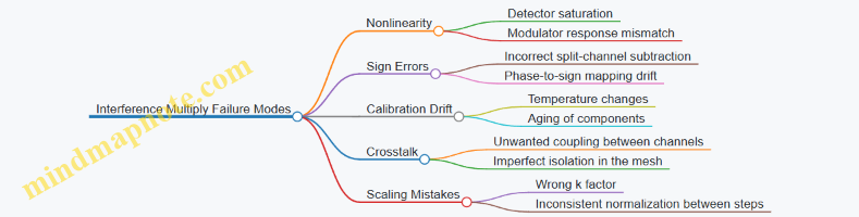
Best Practices Embedded in the Case
- Use a consistent normalization convention for both calibration and inference so the scale factor k is not a moving target.
- Prefer basis-based calibration for small to medium meshes because it directly measures the effective transform rather than relying on ideal component models.
- Validate with signed test vectors even if your training data is mostly positive; sign handling is where “it looks fine” often hides a real error.
- Add bias digitally after detection. Bias is constant per output channel, so doing it in software avoids forcing the optical network to represent an extra affine term.
This small example generalizes: once you can reliably map basis inputs to calibrated outputs, the interference network behaves like a programmable matrix multiplier, and the rest is careful bookkeeping—scales, signs, and verification.
11.2 Case Study: Waveguide Mesh Implementation With Quantized Weights
This case study shows how a small waveguide mesh can implement a quantized-weight linear layer, end to end: from choosing a mesh topology, to mapping weights into phase shifters, to validating the realized matrix with measured transfer functions. The goal is not to “make it work somehow,” but to make the quantization and the calibration assumptions explicit so the results are reproducible.
Problem Setup
Assume a fully connected layer with input vector \(x\in\mathbb{R}^4\) and output \(y\in\mathbb{R}^4\): \[ y = W x \] We choose a mesh that realizes a complex-valued linear transform \(U\) on optical fields, then use detection and encoding so the effective real-valued matrix matches \(W\) as closely as possible.
Quantization choice. Let weights be quantized to \(b=3\) bits signed integers, then scaled to a fixed-point range. A practical rule: quantize after training with a scale chosen so the largest magnitude weight maps near the representable maximum without saturating.
Best practice. Keep the quantization scale and the optical detection scaling tied together. If you quantize \(W\) but later normalize outputs differently, you’ll “fix” an error that was never actually corrected.
Mesh Architecture and Signal Model
We use a square \(4\times 4\) programmable mesh that implements a unitary-like transform \(U\) through a sequence of tunable couplers and phase shifters. In practice, the implemented transform is \(\tilde{U}\), and the difference \(\Delta U=\tilde{U}-U\) comes from loss, finite extinction, and phase errors.
To connect optical fields to the real matrix multiply, we use a standard approach: encode inputs into optical amplitudes, let the mesh apply \(\tilde{U}\), then detect intensities with a calibration model that maps detected signals back to the desired linear operation.
Best practice. Treat the mesh as a linear operator on complex fields, but treat the detector pipeline as a calibrated linear map on the quantities you actually use for inference.
Quantized Weight Mapping into Phase Settings
A common implementation strategy is to decompose the target transform into elementary rotations. For a \(4\times 4\) mesh, the decomposition yields a set of angles \(\theta\) and phases \(\phi\) that control each tunable element.
Quantization step. Quantize the target matrix \(W\) first, then compute the corresponding target optical transform parameters. This avoids the mismatch where the optical settings are derived from floating weights but the inference uses quantized weights.
Example. Suppose one effective rotation in the decomposition corresponds to a mixing coefficient \(c=\cos\theta\). If you quantize the weight matrix so that the implied \(c\) lands on a discrete set, you can quantize \(\theta\) by mapping it to the nearest allowed phase-shifter setting.
Best practice. Quantize in the parameter space that the hardware actually controls. If phase shifters have \(N\) discrete steps, quantize \(\phi\) to those steps early, then propagate the effect into the predicted matrix.
Calibration Workflow with Quantized Targets
Calibration estimates the realized transform \(\tilde{U}\) from measured responses. With quantized weights, you can reduce calibration effort by focusing on the discrete set of settings you will actually use.
- Measure element response. For each tunable element, sweep phase settings across the discrete grid and record output intensities for known input excitations.
- Fit a transfer model. Build a mapping from phase settings to effective complex coefficients. Even a simple linear-in-parameters model can work if you keep the operating range narrow.
- Assemble the full realized matrix. Combine the fitted element models according to the mesh connectivity to predict \(\tilde{U}\).
- Validate with a small test set. Use a handful of input vectors \(x\) with known values, compute predicted \(\hat{y}\), and compare to the expected \(y\) from the quantized \(W\).
Best practice. Validate using inputs that stress the quantization boundaries, not just random small values. For instance, include vectors with entries at \({-1,0,1}\) so sign and saturation effects show up clearly.
Mind Map: Waveguide Mesh Implementation with Quantized Weights
Worked Micro-Example: One Quantized Rotation
Consider a single mixing stage in the decomposition that should implement a coefficient \(c\). Hardware provides phase settings \(\phi\in{0,\Delta,2\Delta,\dots}\). After quantization, the desired \(c\) corresponds to a phase \(\phi^*\) that is not on the grid.
- Choose \(\phi_{q}=\arg\min_{\phi\in\text{grid}}|c(\phi)-c(\phi^*)|\).
- Predict the resulting effective matrix \(\hat{W}\) using the fitted element model.
- Confirm by measuring the output for a basis input vector (one-hot input). If the measured response matches the predicted response within tolerance, the mapping rule is consistent.
Best practice. Use one-hot inputs during validation because they isolate columns of the effective matrix, making it obvious whether the error is a column scaling issue or a mixing-angle issue.
Results Interpretation and Practical Guardrails
When quantization is done correctly, the dominant errors usually come from two places: (1) phase quantization granularity and (2) calibration model mismatch under loss and crosstalk. Guardrails that keep the case study honest:
- Track an explicit effective matrix \(\tilde{W}\) derived from measured responses, not just from predicted \(\tilde{U}\).
- Keep the same quantized weight set during calibration and validation.
- Report error as both a matrix-level metric (how close \(\tilde{W}\) is to \(W\)) and a task-level metric (how close \(\tilde{y}\) is to \(y\) for the test inputs).
This structure turns the mesh from a black box into a calibrated linear operator whose quantization assumptions are visible, testable, and repeatable.
11.3 Case Study: Calibration and Error Correction in Practice
A practical calibration goal is simple to state: make the implemented optical transform match a target matrix closely enough that inference accuracy stops improving when you try harder. The tricky part is that calibration is not a one-time ritual; it is a controlled measurement loop that must account for drift, quantization, and measurement noise.
Calibration Setup and Baseline Measurements
Start with a small mesh tile that implements a known linear transform. Use a test matrix with distinct rows so you can tell if errors are row-mixing (wrong interference) versus column-scaling (encoding or detection mismatch). Drive the mesh with a set of input basis vectors, one at a time, and record the detected outputs.
Best practice: normalize your measurement so each input basis vector has the same optical energy at the chip input. If you do not, your “matrix” will accidentally include power calibration errors, and later correction will chase the wrong problem.
Concrete example: for a 4×4 tile, inject four basis vectors, measure four output vectors, and assemble an estimated transfer matrix \(\hat{T}\). If your target is \(T\), the initial error is \(E = \hat{T} - T\). Track both magnitude error and phase-consistency error; phase mistakes can look small in intensity but still break interference.
Mind Map: Calibration and Error Correction Workflow
Error Mode Identification
Before correcting, classify what went wrong. In photonic meshes, the most common issues are: (1) phase shifter offsets, (2) amplitude imbalance from loss or coupler imperfections, and (3) cross-coupling that causes unintended mixing.
A systematic way to separate these: compare two reconstructions. First, reconstruct \(\hat{T}\) directly from measured basis responses. Second, reconstruct a “phase-only” model by normalizing each measured output vector to remove amplitude differences. If the phase-only reconstruction improves accuracy substantially, amplitude errors are likely dominant; if it barely changes, phase and interference structure are the main culprits.
Concrete example: suppose your measured outputs for input basis \(e_1\) have the right interference pattern but consistently lower magnitude across all outputs. That points to global or per-channel loss, which you can correct with scaling rather than re-tuning every phase shifter.
Correction Loop with Regularized Updates
A correction loop updates control parameters (phase shifter settings, and optionally per-channel gain factors). The simplest approach is to compute a parameter delta that reduces \(|\hat{T} - T|\) under a linearized model.
Best practice: regularize. Without regularization, the solver can “fit” detector noise, producing a transfer matrix that looks better on the calibration vectors but worse on new inputs.
Concrete example: use a small set of calibration vectors (basis vectors plus a few random superpositions) and reserve held-out vectors for verification. If the correction improves held-out performance, you are correcting the device; if it only improves calibration vectors, you are correcting the noise.
Worked Example: From Measured Matrix to Corrected Behavior
Assume the target tile is a known 4×4 unitary-like transform. After baseline measurement you obtain \(\hat{T}\). You compute a corrected estimate \(\hat{T}_{\text{corr}}\) by applying two compensations:
- Amplitude scaling compensation: estimate a per-output gain \(g\) so that \(g \odot \hat{T}\) better matches \(T\) in least-squares sense. This handles loss imbalance.
- Phase shifter update: adjust phase settings using a linearized sensitivity model derived from small perturbations around the current settings.
Verification uses held-out inputs: for each held-out vector \(x\), compare predicted outputs \(T x\) versus corrected outputs \(\hat{T}_{\text{corr}} x\). Use an error metric that reflects inference relevance, such as mean squared error on normalized outputs.
Stability Checks and Practical Recalibration Triggers
Even after a good calibration, you need to know when it stops being good. Stability checks should be lightweight: re-measure a small subset of basis vectors and compute whether the error metric crosses a threshold.
Best practice: define triggers based on the metric you actually care about, not on raw detector drift. If your inference pipeline normalizes activations, then a global gain drift might not matter; interference pattern drift does.
Concrete example: if re-measuring two basis vectors shows the same relative interference ratios but the absolute magnitude changes, you can update scaling without re-running the full phase calibration.
Summary of What Works in Practice
Effective calibration is measurement normalization, error-mode identification, regularized correction, and verification on held-out vectors. The “error correction” part is not a single algorithm; it is a disciplined loop that prevents you from mistaking noise and power drift for interference mistakes.
11.4 Case Study: End to End Inference Pipeline with Photonic Acceleration
This case study walks through a complete inference path for a small neural network layer implemented on an optical waveguide mesh. The goal is not just “it runs,” but “it runs with predictable accuracy and controlled energy.”
System Setup and Data Path
We assume a single photonic tile performs a linear transform (Y = XW) for a batch of inputs, followed by a digital nonlinearity. Inputs are encoded as optical intensities, weights are encoded as programmable phases and couplings in the mesh, and outputs are detected as photocurrents.
Integrated best practice: keep the boundary between analog and digital operations explicit. In practice, the photonic tile produces a vector of real-valued pre-activations, and the host applies bias addition, activation, and any residual connections.
Example: Suppose the layer maps 8 inputs to 4 outputs. The host prepares 8 real numbers per sample, scales them to a nonnegative intensity range, and sends them as 8 optical channels into the tile. The tile outputs 4 detected values, which the host rescales back to the expected numeric range.
Encoding Strategy and Sign Handling
Optical intensity is naturally nonnegative, so negative weights or activations require a representation choice.
Best practice: use a two-channel differential encoding for signed values. Represent each scalar (v) as \((v = v^+ - v^-)\) with \((v^+, v^- \ge 0)\). The mesh computes linear combinations on both channels, and the host subtracts detected outputs.
Example: If an activation (v=-0.3), encode \((v^+=0)\) and \((v^-=0.3)\). After detection, compute \((y = y^+ - y^-)\). This keeps the optical hardware operating in its comfortable nonnegative regime.
Weight Programming and Calibration Loop
The mesh is a linear optical system whose programmed settings correspond to a target transfer matrix. Real devices drift, so calibration is part of inference, not a one-time chore.
Best practice: calibrate to the exact matrix used for inference, including scaling factors from your encoding. Use a small set of probe vectors to estimate the effective transfer matrix \( \tilde{W} \).
Example: For the 8-to-4 layer, probe with basis-like inputs that isolate each input channel’s contribution. Measure the 4 outputs per probe, fit the effective matrix, and store a correction matrix (C) such that (XW \approx X\tilde{W}C). Apply (C) in the host after detection.
Inference Execution Steps
A practical inference loop has five stages.
- Preprocess and scale inputs. Convert activations to the chosen encoding range and apply the same scaling used during training.
- Generate optical channels. Map each encoded scalar to a channel amplitude or intensity.
- Run the photonic transform. Program the mesh once per layer (or per weight update), then stream batches through.
- Detect and postprocess. Convert photocurrents to digital values, apply differential subtraction if used, and apply calibration correction.
- Apply digital nonlinearity. Compute bias, activation (e.g., ReLU), and any normalization steps not implemented optically.
Example: For a batch of 32 samples, the host streams 32 encoded vectors. The tile outputs 4 detected values per sample. The host subtracts differential outputs, adds bias, and applies ReLU.
Error Budget and Verification Metrics
To keep accuracy stable, track errors at each boundary.
Best practice: separate “optical linearity error” from “numeric scaling error.” Optical linearity error shows up as mismatch between the measured effective matrix and the target. Scaling error shows up when encoding/decoding ranges differ from what the model expects.
Example metrics:
- Matrix error: \( |W-\tilde{W}C|_F / |W|_F \)
- Output drift: mean and variance of output residuals on a fixed validation batch
- Activation mismatch: fraction of elements whose sign changes before ReLU
Mind Map: End to End Inference Pipeline
Minimal Worked Example with Numbers
Assume the host expects (y = XW + b) with \((W\in\mathbb{R}^{8\times 4})\). Use differential encoding for inputs.
- Host encodes each input channel (x_i) into \(x_i^+\) and \(x_i^-\).
- The mesh computes two detected vectors \(\hat{y}^+\) and \(\hat{y}^-\).
- Host computes \(\hat{y}=\hat{y}^+ - \hat{y}^-\), then applies correction (C) and adds bias.
Best practice: validate the pipeline with a “known vector” test. Pick a sparse input where only one channel is nonzero. The expected output should match the corresponding column of the effective matrix after correction. This catches channel ordering mistakes and scaling mismatches quickly.
Practical Takeaways
A reliable end-to-end pipeline treats calibration, encoding, and scaling as a single coupled system. When the host applies correction and the digital tail handles nonlinearities, the photonic tile can stay focused on its job: fast, linear transforms with controlled error.
11.5 Case Study: Energy Measurement Methodology and Results Interpretation
This case study measures energy for a photonic matrix multiply layer and explains how to interpret the numbers without fooling yourself. The goal is to separate three contributors: optical energy delivered to the chip, electrical energy used to set and stabilize the optical configuration, and electrical energy consumed by detection and readout.
Measurement Setup and What You Must Decide First
Start by defining the exact operation you are timing and powering. For example, choose a single inference pass through one linear layer implemented by a waveguide mesh. Fix the batch size to 1 so you can see per-sample energy clearly.
Next, decide what “energy per multiply” means. A practical definition is:
- Energy per output element: total system energy divided by the number of multiply-accumulate operations that produced one output vector element.
- Energy per MAC: energy per output element divided by the number of input terms contributing to that element.
If your layer is an M×K times K×N multiply, then total MACs per sample are M·N·K. Keep this arithmetic visible; it prevents the classic mistake of dividing by the wrong count.
Instrumentation Plan
Use three measurement channels.
- Optical power and duration: measure laser output power at the chip input and multiply by the optical on-time. If you cannot measure at the chip, measure at the laser output and include a calibrated insertion loss term.
- Control electronics power: measure the power drawn by phase shifter drivers and any bias networks. If the drivers have separate rails, measure them individually and sum.
- Detection and readout power: measure photodetector bias power and the power of the transimpedance amplifiers and ADCs used to digitize outputs.
A good best practice is to record power in two regimes: configuration (when phases are being tuned) and execution (when the optical inputs are applied and outputs are read). Many systems look efficient only if you average configuration energy over many inferences.
Example Measurement Procedure for One Layer
Assume a 64×64×64 layer (M=64, K=64, N=64). Suppose you run 1000 inferences with the same calibrated mesh settings.
- Optical energy: if chip input optical power is 2.0 mW and execution time is 1.0 µs, optical energy per inference is 2.0 mW × 1.0 µs = 2.0 nJ.
- Control energy: if driver power during execution is 0.5 W and execution time is 1.0 µs, execution control energy is 0.5 µJ? Careful: 0.5 W × 1.0 µs = 0.5 µJ? Actually 0.5 W × 1e-6 s = 0.5 µJ, which is 500 nJ. That dwarfs optical energy, so you must confirm whether drivers truly draw that much during execution or only during updates.
- Configuration energy amortization: if calibration takes 10 s and the control power during tuning is 1.0 W, configuration energy is 10 J. Amortized over 1000 inferences, that is 10 mJ per inference = 10,000,000 nJ, which is enormous. In practice, you would either reduce tuning frequency, reduce tuning duration, or redesign control so it draws less during calibration.
This is why you must report both per-inference execution energy and amortized energy including calibration.
Mind Map: Energy Measurement and Interpretation
Results Interpretation Without Hand-Waving
Once you compute energy per MAC, interpret it by identifying the dominant term.
- If optical energy is tiny compared to control energy, then the system is limited by static or hold power in the phase shifter drivers. A common fix is to measure driver behavior during hold and ensure you are not overestimating.
- If configuration energy dominates, then your calibration cadence is too frequent for the workload. The interpretation should state the amortization assumption explicitly: “1000 inferences per calibration.”
- If detection energy dominates, then the limiting factor is often the ADC sampling rate and the number of output channels digitized per inference.
A final best practice is to include a sanity check using scaling. For instance, if you double execution time while keeping power constant, energy per inference should double, and energy per MAC should also double. If it does not, you likely measured the wrong window or mixed configuration and execution.
Worked Summary for the 64×64×64 Example
For the same 1000-inference reuse assumption, report:
- Execution-only energy per inference: optical + control-hold + detection/readout.
- Amortized energy per inference: execution-only + (configuration energy / 1000).
- Energy per MAC: divide each per-inference total by M·N·K = 64·64·64.
This structure keeps the story consistent: you can see whether the layer is energy-efficient because of optics, because of reuse, or because the electronics are behaving better than expected. And yes, it also makes it harder for unit mistakes to sneak in and ruin the party.
12. Design Methodology for Minimal Energy Neural Multiplication
12.1 Selecting Matrix Sizes and Tiling for Efficiency
Photonic matrix multiplication is efficient when you keep the optical work “busy” while minimizing wasted power in unused paths. The two knobs that matter most are matrix size (how many multiply-accumulate operations you pack into one optical transform) and tiling (how you split a larger layer into smaller transforms that fit the hardware).
Start with the Hardware Reality
A waveguide mesh implements a linear transform with a fixed number of inputs and outputs. If your target layer needs a weight matrix of shape \(W\in\mathbb{R}^{M\times N}\), you must choose a tiling that maps \(N\) input features and \(M\) output features onto the mesh ports.
A practical rule: pick tile sizes \(N_t\) and \(M_t\) that match the mesh dimensions (or a convenient subset) so you avoid padding with zeros. Padding is not free in optics because it still consumes dynamic range, calibration effort, and sometimes detection bandwidth.
Easy example: Suppose the mesh has 16 inputs and 16 outputs. Your layer has \(M=64\), \(N=48\). Choose \(N_t=16\) and \(M_t=16\). Then you need \(64/16=4\) output tiles and \(48/16=3\) input tiles. Each output tile accumulates results from three input tiles.
Tiling Strategy That Minimizes Accumulation
Each tile multiplication produces partial sums. The way you order tiles affects how many times you must accumulate at the detector or in the digital host.
For photonic systems, accumulation cost is often dominated by how many times you must read out and sum partial results. A good default is output-stationary tiling: keep \(M_t\) fixed while sweeping over \(N_t\). That way, each output tile collects all contributions for its rows.
Easy example: With the same \(M=64\), \(N=48\) and \(16\times16\) mesh, output-stationary tiling means you compute one \(16\times16\) block for each of the three input tiles, then sum them to form a final \(16\times16\) output block. If you instead sweep outputs first, you may increase the number of intermediate readouts depending on your host pipeline.
Match Tile Size to Detection and Noise
Larger tiles reduce the number of tiles, but they can increase the optical power required to keep signal above noise. Detection noise includes shot noise and readout noise; both interact with how you scale intensities to represent values.
A systematic approach:
- Choose \(N_t\) so that the input encoding uses the available dynamic range without saturating.
- Choose \(M_t\) so that each output channel has enough optical power to maintain acceptable signal-to-noise ratio.
- If you must trade off, prefer increasing \(M_t\) over \(N_t\) when your encoding is input-power limited, because output channels can often be normalized per channel.
Easy example: If your encoding maps values to intensity and your laser power budget is tight, you may find that \(N_t=32\) forces you to reduce per-feature intensity, lowering SNR. In that case, using \(N_t=16\) can be more energy-efficient overall even though it increases tile count.
Use a Simple Efficiency Model
Efficiency is not just “fewer tiles.” A useful mental model is:
- Compute work per tile: proportional to \(M_t\times N_t\).
- Tile overhead: proportional to the number of tile launches and readouts.
- Loss and noise penalty: grows when you push encoding harder.
You can estimate total energy for a layer as: \[ E \approx T\cdot E_{launch} + (\text{optical power per launch})\cdot(\text{number of launches}) + E_{host,sum} \] where \(T\) is the number of tiles. Even without exact constants, this model helps you compare candidate \((M_t,N_t)\) choices.
Mind Map: Matrix Sizes and Tiling for Efficiency
Worked Example with Edge Tiles
Assume again a \(16\times16\) mesh, but now your layer is \(M=50\), \(N=34\).
- Output tiles: \(\lceil 50/16\rceil=4\) with sizes \(16,16,16,2\).
- Input tiles: \(\lceil 34/16\rceil=3\) with sizes \(16,16,2\). This yields \(4\times3=12\) tile launches. The two small edge tiles (with size 2) may be less energy-efficient if you still pay the full launch cost, so you can consider regrouping features to reduce the number of tiny tiles.
Easy example: If your layer allows reordering of channels without changing semantics (common in some architectures), you can pack the last 2 features into a tile that also contains other “edge” features from a neighboring block, reducing the number of 2-wide tiles.
Practical Checklist
- Prefer \((M_t,N_t)\) that match mesh ports or clean divisors of \(M\) and \(N\).
- Use output-stationary tiling when you want to minimize intermediate accumulation readouts.
- Avoid padding-heavy designs; use smaller edge tiles when needed.
- Validate that encoding scaling for \(N_t\) and \(M_t\) keeps SNR acceptable without saturating.
- Compare candidates using a simple energy model that counts launches and readouts, not just arithmetic work.
12.2 Choosing Encoding and Detection to Minimize Required Optical Power
Optical power is the bill you pay for getting enough signal at the photodetector. The trick is to choose an encoding and a detection model that (1) uses the available optical degrees of freedom efficiently, (2) avoids wasting photons on irrelevant components, and (3) keeps the mapping from optical fields to numerical values as close to linear as possible.
Start with What “Enough Signal” Means
A photodetector converts optical power into an electrical current. If shot noise dominates, the signal-to-noise ratio (SNR) scales roughly with the square root of detected photon number. That means doubling SNR typically requires about 4× detected photons. So minimizing optical power is mostly about maximizing detected photons per useful numerical effect.
A practical way to reason is to separate the chain into: input encoding → optical transformation → detection and scaling. Each stage can either concentrate the useful signal or spread it into parts you later ignore.
Encoding Choices That Control Photon Efficiency
Intensity-only encoding uses optical power proportional to the value. It is simple, but it often forces you to represent signed numbers using extra channels (e.g., positive and negative parts). Those extra channels double the required optical power for the same effective dynamic range.
Complex field encoding uses both amplitude and phase. In interference-based multiplication, the output intensity depends on the relative phase between paths. This can represent signed weights without splitting into two channels, which can reduce total optical power. The catch is that phase errors and imperfect interference can turn “useful signal” into “wasted leakage.”
Balanced encoding is a middle ground: you still use two channels, but you design them so that common-mode optical power cancels at detection. The goal is to make the detector subtract two correlated signals, improving effective SNR without requiring proportionally more optical power.
Mind Map: Encoding and Power
Detection Choices That Match the Encoding
Detection determines how optical information becomes numbers. If your encoding produces a quantity proportional to the target multiply-accumulate (MAC), then you can keep detection scaling straightforward and avoid extra gain stages.
Direct intensity detection measures optical power at each output waveguide. It is robust and easy to implement, but it assumes your encoding already arranged for the desired numerical relationship to appear in intensity.
Differential detection subtracts two photodetector currents. This is especially effective when your encoding uses complementary channels for positive/negative values or when you use balanced encoding. Differential detection can reduce the impact of common-mode noise and can improve effective SNR for the same optical power.
Normalization-aware detection uses known reference levels to rescale outputs. For example, if you include a calibration tone or a fixed reference path, you can estimate gain and reduce the need for high optical power just to overcome uncertainty in detector gain.
Mind Map: Detection and Power
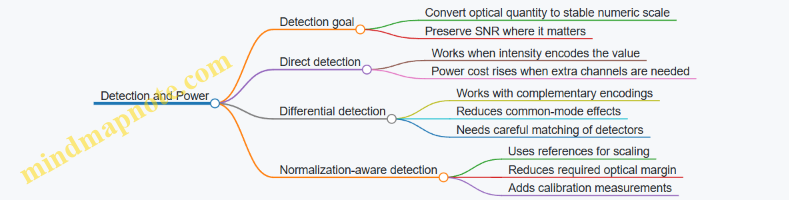
A Systematic Selection Workflow
- Decide where sign lives. If you want signed weights or activations, choose whether sign is encoded in intensity (two-channel) or in phase (single-channel complex field).
- Match detection to the sign strategy. Two-channel intensity sign usually pairs with differential detection. Phase-based sign can often use direct detection if interference is well controlled.
- Set the dynamic range target. Choose an encoding scale so that typical values sit away from detector saturation and away from the noise floor. This is where “minimal power” becomes a concrete number: you pick the smallest optical power that keeps the smallest meaningful signal above noise.
- Account for calibration-induced loss. If phase encoding requires frequent recalibration, the effective power budget must include the optical margin needed to tolerate residual mismatch.
Worked Example: Two Encodings for Signed Weights
Suppose you need to compute a dot product where weights can be positive or negative. You have two options.
Option A: Intensity with two channels. Represent each weight as \((w^+ = max(w,0))\) and \((w^- = max(-w,0))\). The optical network computes contributions for both channels, and you subtract detector currents: \((y \propto I^+ - I^-)\). For the same numerical range, both channels must carry comparable optical power when weights are near zero-crossing, so total detected photons can be roughly doubled.
Option B: Phase-based signed encoding. Encode weight sign by shifting phase by π while keeping a single channel magnitude proportional to (|w|). Interference at the outputs produces an intensity proportional to the signed contribution, so you avoid the second channel. If phase error is small, you get a power reduction close to the channel-count reduction. If phase error is large, leakage increases and you may need extra optical power to maintain SNR.
The selection rule is simple: if your phase control and interference balance are good enough that leakage stays below the noise floor, phase-based encoding wins on optical power. If not, two-channel intensity with differential detection can be more predictable.
Practical Best Practices That Reduce Optical Power
- Use differential detection when you already have complementary channels. It turns subtraction into a noise-aware operation rather than a post-processing guess.
- Keep the encoding scale conservative but not timid. Place typical signals in the detector’s linear region; avoid spending power to lift everything when only the smallest values need it.
- Prefer encodings that align with the detection model. If detection measures intensity, design encoding so the target MAC appears in intensity with minimal extra transformations.
- Calibrate the parts that affect SNR most. For phase encoding, focus on phase offset and path imbalance; for intensity encoding, focus on detector matching and channel gain.
Mind Map: Decision Summary
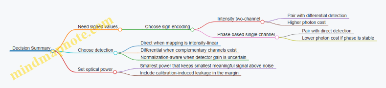
12.3 Balancing Loss, Noise, and Control Energy in Co-Design
Photonic matrix layers rarely fail because the math is wrong; they fail because the physical implementation spends energy in the wrong places. Co-design means you treat loss, noise, and control energy as one coupled system: changing how you encode signals changes required optical power, which changes shot noise, which changes how accurately you must set phases, which changes control energy.
Start with a Single Layer Budget
Define three budgets for one matrix-vector multiply (MVM):
- Optical energy: input optical power times integration time.
- Detection energy: photodiode responsivity, transimpedance gain, and any analog-to-digital conversion energy.
- Control energy: energy to set and hold phase shifters and any calibration overhead.
A practical best practice is to write a “dominant term” assumption before you simulate. For example, if your layer is loss-dominated, you can ignore some quantization details; if it is noise-dominated, you must model detector noise and phase setting error together.
Loss: The Hidden Multiplier
Loss reduces effective signal amplitude at the detector. In coherent interference, amplitude loss is not just a scale factor; it changes how much optical power you need to reach the same signal-to-noise ratio (SNR).
A concrete example: suppose your waveguide mesh has 6 dB insertion loss across the path from input to output. That is a factor of 4 reduction in power. If you keep the same input power, your detected photocurrent drops by 4, and shot noise drops only with the square root of photocurrent. Net effect: SNR falls roughly by a factor of 2 unless you increase input power.
Best practice: treat loss as a design constraint on encoding and detection. If you can choose a detection scheme that tolerates lower amplitude (for instance, by using differential measurement), you may reduce required optical power and indirectly reduce control energy because you can relax phase precision.
Noise: Where It Enters the Computation
Noise sources typically include:
- Shot noise from finite detected photons.
- Thermal noise from electronics.
- Phase noise and drift that turn a programmed unitary into a slightly different one.
A useful way to connect noise to control is to translate phase error into an effective weight error. If a phase shifter has an RMS error \(\sigma_\phi\), then interference terms shift, producing output perturbations that resemble additive noise on the computed dot products.
Best practice: measure or estimate noise in the same units you optimize. If your training objective is classification accuracy, you can still compute an intermediate metric like “effective weight noise variance” and use it to set phase resolution and refresh cadence.
Control Energy: The Cost of Being Precise
Control energy comes from driving phase shifters and from any periodic recalibration or refresh. Two knobs matter:
- Phase resolution: finer steps reduce weight error but require more control effort and may increase sensitivity to drift.
- Update rate: frequent updates track drift but cost energy and can complicate synchronization.
A concrete example: imagine two operating points.
- Option A uses higher optical power so you can tolerate larger phase error. Control energy is lower because you set phases with coarser quantization.
- Option B uses lower optical power to save optical energy, but then you need tighter phase setting and more frequent refresh to prevent noise from dominating.
The “right” choice depends on which energy term is expensive in your system. Co-design compares total energy, not just optical power.
Coupled Tradeoffs as a Mind Map
Mind Map: Loss, Noise, Control Energy Co-Design
A Systematic Co-Design Procedure
- Choose an encoding and detection model that maps optical power and phase settings to an output distribution. Keep it simple enough to compute quickly.
- Estimate loss to determine how much optical power reaches the detector. Convert loss into detected photocurrent.
- Compute noise at the detector for your integration time and bandwidth. Include shot and thermal noise, then add phase-error-induced variance.
- Translate phase-error tolerance into control requirements. If output variance exceeds your accuracy budget, tighten phase quantization or increase refresh frequency.
- Compute total energy: optical input energy plus control energy plus detection/control overhead. Compare against alternatives.
- Validate with a small simulation on a representative layer. Use the same energy-aware settings you derived from the budget.
Worked Example: Choosing Between Optical Power and Phase Precision
Assume a target output SNR of 20 dB for a layer. You measure total insertion loss of 5 dB, so detected power is reduced by about 3.16×. If you double input optical power, detected power doubles, improving shot-noise-limited SNR by \(\sqrt{2}\). Alternatively, if you keep optical power fixed but reduce phase quantization step so that phase RMS error drops by \(\sqrt{2}\), the interference error variance drops by about 2×, improving effective dot-product SNR.
Now compare energy: doubling optical power increases optical energy linearly, while halving phase step may increase control energy sublinearly or linearly depending on the phase shifter driver and update schedule. Co-design selects the option with lower total energy while meeting the same SNR target.
The key point is that loss sets the baseline photocurrent, noise sets the required SNR, and control energy sets how you achieve that SNR without wasting power. When you treat them as a single loop, the “best” setting becomes a straightforward optimization rather than a guess.
12.4 Building a Repeatable Design Checklist for Photonic Layers
A repeatable checklist turns photonic matrix design from a one-off art project into a repeatable engineering process. The goal is simple: every layer design should start from the same inputs, produce the same intermediate artifacts, and end with the same verification evidence.
Start with Layer Requirements and Hardware Assumptions
First write down what the layer must do and what the hardware is allowed to do. Keep these as explicit constraints so later decisions don’t quietly contradict them.
- Compute target: matrix dimensions, batch size, and whether the layer is dense or structured.
- Numerical target: required accuracy for outputs and acceptable error growth across layers.
- Optical budget: available optical power at the chip input, detector responsivity, and allowable insertion loss.
- Control budget: phase shifter resolution, update rate, and whether calibration can run between runs.
Example: If a layer is 256×256 and you only have enough optical power for a certain signal-to-noise ratio (SNR), you should treat SNR as a hard constraint early, not as something you hope calibration will fix later.
Choose Encoding and Detection as a Co-Design Pair
Encoding and detection are not separate steps. They jointly determine dynamic range, noise sensitivity, and how sign is represented.
- Encoding: intensity-only, complex field with phase, or hybrid schemes.
- Normalization: decide where scaling happens so the detector never saturates.
- Sign handling: pick a method such as differential detection or offset encoding.
- Detection model: include shot noise and detector noise in the same model used for accuracy.
Practice: For each encoding, write a one-line mapping from mathematical values to physical quantities. If you cannot express it in one line, the design will likely drift during implementation.
Convert the Target Matrix into an Implementable Form
Most photonic meshes implement a linear transform, but the target layer may not be directly realizable.
- Decompose: express the desired transform in a form compatible with the mesh (e.g., via unitary-plus-gain structure if your architecture supports it).
- Quantize weights: apply the same quantization model used by the phase shifters or programmable elements.
- Constrain structure: if the mesh supports only certain connectivity, enforce sparsity or block structure.
Example: If weights are quantized to 6-bit values, simulate the quantization before mapping to the mesh. Otherwise, you may calibrate a circuit that can’t represent the intended weights.
Map the Implementable Matrix to a Mesh with Calibration in Mind
Mapping is where many designs become fragile. A good checklist forces you to capture calibration assumptions.
- Mesh topology: select the topology that matches the required matrix size and connectivity.
- Parameterization: define how each tunable element maps to matrix entries.
- Calibration plan: specify which measurements you will take and what you will fit.
- Stability model: decide whether you assume drift between calibration and inference.
Practice: Record the expected number of tunable degrees of freedom and compare it to the number of independent measurements you can realistically collect.
Build a Verification Ladder from Fast Checks to Full Runs
Verification should progress from cheap to expensive, with each rung catching a different class of mistakes.
- Rung 1: Dimensional sanity: confirm shapes, tiling, and routing.
- Rung 2: Ideal math: verify the transform under ideal parameters.
- Rung 3: Nonideal simulation: include loss, phase quantization, and noise.
- Rung 4: Calibration simulation: model imperfect fitting and residual error.
- Rung 5: End-to-end layer test: run with the same preprocessing and postprocessing used in the network.
Example: If ideal math is correct but end-to-end fails, the issue is often scaling, sign handling, or detector saturation rather than the mesh mapping.
Lock the Energy Accounting and Control Overheads
Energy is not only optical power. Control and data movement can dominate if you ignore them.
- Optical energy per inference: include input power, integration time, and losses.
- Detection energy: include readout circuitry energy per sample.
- Control energy: estimate phase update energy and how often updates occur.
- Host overhead: account for any required buffering or synchronization.
Practice: Create a single energy budget table for the layer and reuse it across designs so comparisons are fair.
Produce a Design Packet That Can Be Reused
A repeatable process ends with artifacts that another engineer can pick up without guessing.
- Inputs: layer spec, constraints, and encoding choice.
- Intermediate artifacts: implementable matrix, quantization settings, mesh parameters.
- Calibration evidence: measurement plan and fitting assumptions.
- Verification evidence: results for each rung of the ladder.
- Energy evidence: the final energy budget with assumptions.
Mind Map: Repeatable Checklist Flow
Example: Checklist Applied to a Single Dense Layer
- Write the layer spec: 256×256, target output error tolerance, and available optical power.
- Pick encoding: differential detection with normalization to keep detector current below a chosen fraction of saturation.
- Quantize weights to the phase-control representable set before mapping.
- Map to the mesh topology and define the calibration measurements used to fit phase offsets.
- Run the verification ladder: ideal, nonideal, calibration-aware, then end-to-end with the same scaling.
- Compute energy per inference including control updates and detector readout.
- Save the design packet so the next layer can reuse the same structure with only the layer-specific inputs changed.
Final Checklist Summary
If you can fill every item above without hand-waving, you have a design process that is repeatable. The checklist is complete when the design packet contains both the “what” (parameters and mappings) and the “why” (verification ladder and energy assumptions) in a form that can be audited.
12.5 Worked Example: Co-Design From Target Accuracy To Energy Budget
We’ll co-design a single photonic linear layer that implements a matrix-vector multiply. The goal is to meet a target output error while minimizing total energy per inference for that layer. Assume a layer with shape 256×256, executed as a tiled accelerator with 16×16 output blocks. Each block is realized by a programmable waveguide mesh that implements a linear transform from 16 input channels to 16 output channels.
Step 1: Start with a Target Accuracy Budget
Pick a measurable accuracy target in terms of mean-squared error (MSE) at the layer output. Suppose the floating-point reference produces outputs y, and the photonic output produces ŷ. Set a layer-level budget: MSE(ŷ, y) ≤ 1.0e-3.
Split the budget into three contributors that map cleanly to design knobs:
- Weight representation error from quantization and constrained optical weights: 4.0e-4
- Optical transfer error from calibration residuals and phase quantization: 4.0e-4
- Readout noise and scaling mismatch: 2.0e-4
This split is not magic; it just prevents one knob from silently doing all the work.
Step 2: Choose an Encoding and Detection Model
Use intensity encoding for inputs and coherent interference for the linear transform. A practical model is:
- Inputs are normalized to a bounded range, e.g., x in [0, 1].
- The mesh implements an effective complex weight matrix W̃.
- Photodetectors measure output intensities proportional to \(|W̃x|^2\) plus cross terms depending on the architecture.
To keep the math tractable, assume the architecture is operated in a regime where the effective linear mapping is calibrated to behave like y ≈ G·(W_eff x), where G is a gain factor set by optical scaling and detection.
Best practice here: treat G as a calibration variable, not a fixed constant. In the energy budget, G determines how much optical power you need to keep detector noise small.
Step 3: Quantize Weights to Match Optical Constraints
Suppose the mesh can realize weights only with limited phase resolution and limited amplitude control. A simple approach is to train with quantization-aware constraints so the effective weight matrix W_eff is close to the desired W.
Example practice: constrain each effective weight element to a set of K amplitude levels and L phase steps. If K=8 and L=16, you can represent complex weights with 128 discrete states per element. During training, penalize the difference between the ideal output and the photonic model output using the same scaling G you will use at inference.
This targets the first error term. If the quantization-aware training yields an empirical quantization MSE of 3.6e-4, you’re within the 4.0e-4 allocation.
Step 4: Allocate Calibration Precision to the Transfer Error
Phase shifters have finite resolution, and calibration leaves residual mismatch. Model the residual transfer error as an effective perturbation ΔW such that W_eff = W + ΔW.
A useful engineering approximation is:
- MSE_transfer ≈ \(||ΔW x||^2\) averaged over representative x.
Example practice: measure the calibrated transfer matrix for one 16×16 block and compute an empirical error metric, then scale it to the full layer using the same input statistics. If the measured transfer MSE per block is 3.9e-4, you’re within the 4.0e-4 allocation.
Step 5: Convert Readout Noise into Required Optical Power
Detector noise includes shot noise and electronic noise. For a photodetector with responsivity R and integration time τ, the detected charge is proportional to optical power P. Shot noise variance scales with the number of detected photons, so it decreases as you increase P.
Set a readout noise target: MSE_readout ≤ 2.0e-4. Use a simple proportional model:
- MSE_readout ≈ c / (P·τ)
where c is determined from detector parameters and the chosen normalization of x and y. Example practice: if your lab characterization gives c = 2.0e-6 (in consistent units) and τ is fixed at 10 ns, then you need P such that 2.0e-6/(P·10e-9) ≤ 2.0e-4, which implies P ≥ 1.0e-3 W per block.
Now you have a concrete power requirement tied to the noise budget.
Step 6: Compute Energy per Layer and Optimize the Knobs
Energy per layer is dominated by optical power delivery plus control energy for reconfiguration. For inference with fixed weights, control energy is mostly calibration amortized; optical power dominates.
Assume:
- Number of blocks: (256/16)×(256/16) = 256 blocks
- Optical power per block: P = 1.0 mW
- Integration time: τ = 10 ns
- Optical delivery efficiency: η = 0.5 (includes coupling and propagation losses)
Optical energy per layer:
- E_opt ≈ (P/η)·τ·256
- E_opt ≈ (1.0e-3/0.5)·10e-9·256 ≈ 5.12e-9 J
Control energy: if phase shifters are static during inference, add a small per-layer overhead for synchronization and readout electronics. Suppose it totals 0.5e-9 J. Then E_total ≈ 5.62e-9 J.
Optimization loop: if you reduce optical power, readout noise increases and may violate the 2.0e-4 term. If you increase phase resolution or improve calibration, you can reduce required optical power because you can reduce scaling mismatch and effective noise amplification. In practice, you iterate by re-estimating the three MSE terms and recomputing the power needed for the readout term.
Mind Map: Co-Design from Accuracy to Energy
Worked Summary with Numbers
- Quantization MSE: 3.6e-4 (pass)
- Transfer MSE: 3.9e-4 (pass)
- Readout MSE target: 2.0e-4 achieved with P ≥ 1.0 mW
- Total energy per 256×256 layer: about 5.62 nJ
The key takeaway is that energy minimization becomes a constrained optimization problem: you don’t guess power, you earn it by spending accuracy budget where it reduces the required optical signal.