Precision Metrology And Measurement For Semiconductor Manufacturing
1. Introduction to Semiconductor Metrology
1.1 Overview of Semiconductor Manufacturing Processes
Semiconductor manufacturing is a highly complex, multi-step process that transforms raw silicon wafers into fully functional integrated circuits (ICs). Understanding the overall flow of these processes is essential for metrology engineers, process control specialists, and fab engineers to ensure precision measurement and control at every stage.
Key Stages in Semiconductor Manufacturing
- Wafer Fabrication: Creating the semiconductor devices on silicon wafers through multiple photolithography, deposition, etching, and doping steps.
- Assembly and Packaging: Cutting wafers into individual dies, attaching them to substrates, and encapsulating them for protection and connectivity.
- Testing: Electrical and functional testing of devices to ensure performance and reliability.
Mind Map: Semiconductor Manufacturing Process Flow
Detailed Process Breakdown
-
Wafer Fabrication
-
Oxidation: Growing a thin oxide layer on the wafer surface to act as an insulator or mask.
- Example: Thermal oxidation to grow SiO2 layers of controlled thickness.
-
Photolithography: Transferring circuit patterns onto the wafer using light-sensitive photoresist.
- Example: Using deep ultraviolet (DUV) lithography to define transistor gates.
-
Etching: Removing material selectively to create the desired patterns.
- Example: Reactive ion etching (RIE) to form trenches or vias.
-
Ion Implantation: Doping the silicon with impurities to modify electrical properties.
- Example: Implanting boron ions to create p-type regions.
-
Deposition: Adding thin films of materials such as metals or dielectrics.
- Example: Chemical vapor deposition (CVD) of silicon nitride layers.
-
Chemical Mechanical Planarization (CMP): Polishing the wafer surface to achieve flatness.
- Example: Planarizing interlayer dielectrics to ensure uniform layers for subsequent lithography.
-
-
Assembly and Packaging
-
Dicing: Cutting the wafer into individual chips.
- Example: Using a diamond saw to separate dies without damaging them.
-
Die Attach: Mounting the die onto a substrate or lead frame.
- Example: Using conductive epoxy for die attachment.
-
Wire Bonding / Flip Chip: Establishing electrical connections.
- Example: Ultrasonic wire bonding to connect die pads to package leads.
-
Encapsulation: Protecting the chip with molding compounds or ceramic packages.
- Example: Transfer molding to encapsulate the die.
-
-
Testing
-
Wafer Sort: Testing dies on the wafer before dicing.
- Example: Probing transistor functionality to identify defective dies early.
-
Final Test: Comprehensive testing after packaging.
- Example: Burn-in testing to detect early-life failures.
-
Example: Photolithography in Practice
Consider a fab engineer optimizing photolithography:
- Goal: Achieve precise patterning of 7 nm transistor gates.
- Challenge: Minimizing line edge roughness and overlay errors.
- Metrology Role: Using CD-SEM to measure critical dimensions and overlay metrology to ensure layer alignment.
This example highlights how understanding the manufacturing step guides the selection of metrology tools and best practices.
Summary
A clear grasp of the semiconductor manufacturing process flow is foundational for effective precision metrology. Each step presents unique measurement challenges and opportunities for process control. By integrating best practices and real-world examples, metrology professionals can enhance yield, reduce variability, and support advanced technology nodes.
1.2 Importance of Precision Measurement in Semiconductor Fabrication
Precision measurement is the cornerstone of semiconductor fabrication, where the demand for ever-smaller feature sizes and higher device performance pushes the limits of manufacturing capabilities. Accurate and reliable metrology ensures that each process step meets stringent specifications, directly impacting yield, device functionality, and cost efficiency.
Why Precision Measurement Matters
- Ensuring Device Performance: Semiconductor devices rely on nanoscale features; even minor deviations can cause significant electrical performance variations.
- Maintaining Process Control: Real-time measurement feedback enables process adjustments to keep fabrication within control limits.
- Yield Improvement: Early detection of deviations or defects reduces scrap and rework, improving overall yield.
- Cost Reduction: Minimizing variability and defects lowers manufacturing costs by reducing waste and downtime.
- Compliance with Design Rules: Precision metrology verifies that fabricated structures comply with design specifications and industry standards.
Mind Map: Importance of Precision Measurement
Example 1: Critical Dimension (CD) Control in Lithography
In lithography, the critical dimension defines the width of transistor gates or interconnect lines. A deviation of just a few nanometers can lead to threshold voltage shifts or timing issues. By employing precision CD-SEM measurements after lithography, fabs can detect deviations early and adjust exposure dose or focus parameters to bring the process back into control.
Example 2: Overlay Accuracy in Multi-Layer Devices
Modern semiconductor devices consist of multiple layers stacked with nanometer alignment tolerances. Overlay metrology measures the alignment between layers. If overlay errors exceed specifications, devices may malfunction due to short circuits or open connections. Precision overlay measurement allows fabs to correct alignment errors in subsequent layers, ensuring device integrity.
Mind Map: Examples of Precision Measurement Impact
Best Practices Embedded in Precision Measurement
- Regular Calibration: Ensuring measurement tools are calibrated to traceable standards to maintain accuracy.
- Statistical Process Control (SPC): Using measurement data to monitor process trends and detect shifts before defects occur.
- Cross-Tool Correlation: Verifying measurements across different metrology tools to confirm consistency.
- Environmental Control: Maintaining stable temperature, humidity, and vibration conditions to reduce measurement noise.
Practical Example: Implementing SPC for CD Control
A fab implemented SPC charts using CD measurements from inline CD-SEM tools. When the data showed a trending increase in line width, engineers investigated and found a focus drift in the lithography scanner. Correcting the focus restored the CD to target values, preventing yield loss.
Summary
Precision measurement is indispensable in semiconductor fabrication, enabling tight process control, high yield, and device reliability. Integrating best practices and leveraging real-world examples highlights how metrology directly supports manufacturing excellence.
1.3 Key Metrology Parameters and Metrics
In semiconductor manufacturing, precision metrology hinges on accurately measuring and controlling a variety of critical parameters. These parameters directly influence device performance, yield, and reliability. Understanding these key metrology parameters and metrics is essential for metrology engineers, process control specialists, and fab engineers to optimize fabrication processes.
Major Metrology Parameters
- Critical Dimension (CD): The width of features such as transistor gates or interconnect lines.
- Overlay: The alignment accuracy between successive lithographic layers.
- Film Thickness: Thickness of deposited or grown films, including dielectrics and metals.
- Surface Roughness: Microscopic texture of surfaces affecting device behavior.
- Defect Density and Classification: Number and type of defects per unit area.
- Electrical Properties: Parameters such as sheet resistance and contact resistance.
Key Metrics and Their Importance
| Parameter | Metric Examples | Importance in Process Control | Example Application |
|---|---|---|---|
| Critical Dimension | Mean CD, CD Uniformity, CD Variation (3σ) | Ensures device feature sizes meet design rules | Measuring gate length to control transistor speed |
| Overlay | Overlay Error (nm), Overlay Uniformity | Prevents layer misalignment that causes device failure | Aligning multi-layer lithography patterns |
| Film Thickness | Average Thickness, Thickness Uniformity | Controls electrical and mechanical properties | Monitoring oxide thickness for gate dielectrics |
| Surface Roughness | RMS Roughness (nm), Peak-to-Valley Height | Affects interface quality and reliability | Assessing CMP polish quality |
| Defect Density | Defects/cm², Defect Types | Identifies yield-limiting defects | Detecting particles on wafer surface |
| Electrical Properties | Sheet Resistance (Ω/sq), Contact Resistance (Ω) | Validates electrical performance of layers | Measuring resistance of metal interconnects |
Mind Map: Key Metrology Parameters Overview
Practical Examples
Example 1: Controlling Critical Dimension Variation
In a 7nm node process, the transistor gate length must be tightly controlled within ±2nm. Using CD-SEM measurements, engineers monitor the mean CD and 3σ variation across wafers. If variation exceeds limits, lithography focus or exposure dose is adjusted. This feedback loop reduces variability and improves device performance.
Example 2: Overlay Accuracy in Multi-Layer Lithography
A fab producing advanced logic devices uses image-based overlay metrology to measure alignment between layers. An overlay error of 3nm is detected, exceeding the 2nm spec. Engineers analyze the data and find stage calibration drift. After recalibration, overlay error reduces to 1.5nm, preventing yield loss.
Example 3: Film Thickness Uniformity Monitoring
During chemical vapor deposition (CVD) of a high-k dielectric, ellipsometry is used to measure film thickness uniformity across 300mm wafers. A uniformity of ±1% is required. When uniformity degrades to ±3%, process parameters such as gas flow and temperature are optimized to restore uniformity.
Best Practices for Managing Parameters and Metrics
- Define Clear Specifications: Establish tight but achievable control limits for each parameter.
- Regular Calibration: Ensure metrology tools are calibrated to maintain measurement accuracy.
- Statistical Process Control (SPC): Use SPC charts to monitor trends and detect drifts early.
- Cross-Tool Correlation: Validate measurements across different metrology tools to confirm accuracy.
- Data Integration: Combine metrology data with process data for holistic process control.
By mastering these key parameters and metrics, semiconductor fabs can maintain tight process control, reduce variability, and ultimately improve device yield and performance.
1.4 Common Challenges in Semiconductor Metrology
Semiconductor metrology plays a critical role in ensuring device performance, yield, and reliability. However, the field faces several inherent challenges due to the complexity and scale of modern semiconductor manufacturing. Understanding these challenges is essential for metrology engineers, process control specialists, and fab engineers to develop effective measurement strategies and maintain process control.
Key Challenges Overview
Resolution Limits
One of the fundamental challenges in semiconductor metrology is achieving sufficient resolution to accurately measure nanoscale features. Optical metrology tools, such as scatterometry and ellipsometry, are limited by the diffraction limit of light, which restricts their ability to resolve features below a certain size.
Example: Measuring critical dimensions (CD) of features below 10 nm often requires electron beam-based metrology (CD-SEM) because optical tools cannot reliably resolve these dimensions. However, CD-SEM tools have slower throughput and higher cost.
Best Practice: Combine optical metrology for high-throughput approximate measurements with periodic high-resolution CD-SEM measurements for calibration and verification.
Measurement Throughput
In high-volume semiconductor manufacturing, metrology tools must provide rapid measurements without compromising accuracy. Balancing throughput and precision is challenging, especially as device complexity increases.
Example: Inline metrology tools integrated into lithography or etch processes must measure wafers quickly to avoid bottlenecks. For instance, scatterometry tools can measure film thickness and CD rapidly but may require offline tools for detailed defect analysis.
Best Practice: Implement a tiered metrology approach where fast inline tools handle routine measurements, and offline tools perform in-depth analysis on sampled wafers.
Tool Calibration and Drift
Metrology tools can experience drift over time due to mechanical wear, environmental changes, or electronic instability, leading to measurement inaccuracies.
Example: A CD-SEM tool may show gradual measurement drift if not regularly calibrated against certified reference standards, causing false process excursions.
Best Practice: Establish rigorous calibration schedules using traceable standards and implement automated drift detection algorithms to trigger recalibration.
Data Management and Integrity
Modern fabs generate enormous volumes of metrology data. Managing, storing, and analyzing this data while ensuring its integrity is a significant challenge.
Example: A fab measuring multiple parameters across thousands of wafers daily can accumulate terabytes of data. Without proper data governance, critical trends may be missed or misinterpreted.
Best Practice: Utilize centralized data management systems with built-in validation, version control, and secure access. Employ advanced analytics to extract actionable insights.
Process Complexity and Material Variability
Semiconductor devices involve multiple layers with different materials, each requiring specific measurement techniques. Variability in film properties or layer interfaces complicates accurate measurement.
Example: Measuring the thickness of a multilayer stack with varying refractive indices can lead to ambiguous ellipsometry results if the model is not carefully calibrated.
Best Practice: Develop robust optical models and cross-validate measurements with complementary techniques such as TEM or X-ray reflectometry.
Defect Detection Sensitivity
Detecting and classifying defects at the nanoscale is critical for yield improvement but is challenged by the small size and low contrast of defects.
Example: Optical inspection tools may miss sub-50 nm defects or generate false positives due to surface roughness.
Best Practice: Integrate multi-modal inspection combining optical and electron beam methods, and apply machine learning algorithms for improved defect classification.
Environmental Influences
Environmental factors such as temperature fluctuations, vibration, and acoustic noise can adversely affect measurement accuracy.
Example: A vibration from nearby equipment can cause image blur in SEM measurements, reducing resolution.
Best Practice: Design metrology labs with vibration isolation, temperature control, and acoustic dampening to maintain stable measurement conditions.
Summary Mind Map
By understanding and addressing these challenges through best practices and integrated measurement strategies, semiconductor metrology teams can ensure reliable, high-precision measurements that support advanced manufacturing processes.
1.5 Best Practices: Establishing a Metrology-Driven Culture with Real-World Examples
Establishing a metrology-driven culture within semiconductor manufacturing is critical for achieving consistent process control, improving yield, and accelerating innovation. This section explores best practices to embed metrology at the core of your fab operations, supported by practical examples and mind maps to visualize key concepts.
Why a Metrology-Driven Culture Matters
- Ensures measurement data guides process decisions
- Promotes accountability and continuous improvement
- Enables early detection of process drifts and defects
- Facilitates cross-functional collaboration between metrology, process, and fab engineers
Best Practices Overview Mind Map
Data Integrity: The Foundation of Trustworthy Measurements
Key Points:
- Regular calibration and validation of metrology tools.
- Maintaining traceability of measurements to standards.
- Implementing strict tool maintenance schedules.
Example: At a leading semiconductor fab, instituting a monthly calibration routine for CD-SEM tools reduced measurement drift by 30%, directly improving process stability. The fab also implemented a digital logbook to track calibration history, enabling quick audits and root cause analysis.
Training & Education: Empowering Teams
Key Points:
- Conduct cross-functional workshops involving metrology engineers, process engineers, and fab operators.
- Develop certification programs to ensure consistent understanding of metrology principles.
Example: A fab introduced quarterly metrology boot camps where engineers from different departments learned about measurement techniques and data interpretation. This initiative led to a 25% reduction in misinterpretation-related process excursions.
Process Integration: Embedding Metrology in Manufacturing
Key Points:
- Use inline metrology to provide real-time feedback.
- Implement Statistical Process Control (SPC) based on metrology data.
- Establish closed-loop control systems where measurement data directly adjusts process parameters.
Example: An advanced packaging line integrated inline film thickness metrology with deposition tools. Real-time feedback allowed immediate adjustments, reducing film thickness variation by 40% and improving device reliability.
Communication: Transparency and Collaboration
Key Points:
- Share metrology data openly across teams.
- Hold regular review meetings to discuss measurement trends and anomalies.
Example: A fab created a centralized dashboard displaying key metrology KPIs accessible to all stakeholders. Weekly cross-departmental meetings focused on interpreting this data, fostering a proactive approach to process control.
Continuous Improvement: Driving Innovation Through Measurement
Key Points:
- Conduct root cause analysis when measurement deviations occur.
- Organize Kaizen events focused on metrology improvements.
- Pilot new metrology technologies and methodologies.
Example: Following a spike in overlay errors, a fab team performed a root cause analysis revealing vibration issues in the metrology lab. After implementing vibration isolation and updating protocols, overlay accuracy improved by 15%. Additionally, the fab piloted AI-based defect classification tools, reducing manual review time by 50%.
Integrated Mind Map: Metrology-Driven Culture with Examples
Summary
Establishing a metrology-driven culture is a multi-faceted effort involving data integrity, education, process integration, communication, and continuous improvement. Real-world examples demonstrate that embedding these best practices leads to measurable improvements in process control, yield, and innovation capacity. By fostering collaboration and transparency, fabs can leverage metrology as a strategic asset rather than a mere measurement task.
2. Fundamental Measurement Techniques in Semiconductor Metrology
2.1 Optical Metrology: Principles and Applications
Optical metrology is a cornerstone technique in semiconductor manufacturing, leveraging light-matter interactions to measure critical parameters such as dimensions, film thickness, overlay, and defects with high precision and non-contact methods. This section explores the fundamental principles behind optical metrology, its common applications in semiconductor fabs, and practical examples illustrating best practices.
Principles of Optical Metrology
Optical metrology relies on the behavior of light when it interacts with semiconductor materials and structures. Key physical phenomena include reflection, refraction, scattering, diffraction, and interference. By analyzing these interactions, metrology tools extract dimensional and material property information.
Core Concepts:
- Reflection & Refraction: Changes in light direction at interfaces reveal film thickness and refractive index.
- Interference: Constructive and destructive interference patterns help measure nanoscale film thickness.
- Diffraction: Light bending around edges or apertures provides information on feature sizes.
- Scattering: Variations in scattered light intensity relate to surface roughness or defects.
Mind Map: Optical Metrology Principles
Common Optical Metrology Techniques in Semiconductor Manufacturing
-
Ellipsometry
- Measures changes in polarization upon reflection.
- Used for thin film thickness and refractive index determination.
-
Reflectometry
- Measures reflected light intensity versus wavelength or angle.
- Provides film thickness and uniformity data.
-
Scatterometry
- Analyzes diffraction patterns from periodic structures.
- Applied for critical dimension and overlay measurements.
-
Optical Critical Dimension (OCD)
- Uses spectroscopic reflectance and scatterometry data.
- Enables non-destructive CD and profile measurements.
-
Interferometry
- Uses interference of light waves to measure surface topography and film thickness.
Mind Map: Optical Metrology Techniques
Practical Example 1: Using Ellipsometry for Thin Film Thickness Measurement
Scenario: A fab needs to monitor the thickness of a silicon dioxide (SiO2) layer deposited on wafers to ensure it meets design specifications.
Approach:
- An ellipsometer shines polarized light onto the wafer surface.
- The change in polarization state after reflection is measured.
- Using a model of the film stack, the thickness and refractive index are extracted.
Best Practice: Regularly calibrate the ellipsometer with reference samples and validate measurements against cross-sectional SEM to ensure accuracy.
Practical Example 2: Scatterometry for Critical Dimension Control
Scenario: Controlling the linewidth of photoresist patterns during lithography.
Approach:
- Scatterometry tools illuminate periodic grating patterns with broadband light.
- The diffraction pattern is collected and analyzed.
- The CD and sidewall angle are extracted by fitting the data to rigorous coupled-wave analysis (RCWA) models.
Best Practice: Integrate scatterometry measurements inline to provide real-time feedback for lithography process adjustments, reducing CD variability.
Best Practices for Optical Metrology Implementation
- Calibration & Validation: Use certified reference materials and cross-verify with complementary metrology tools.
- Environmental Control: Maintain stable temperature, vibration isolation, and cleanroom conditions to minimize measurement noise.
- Model Accuracy: Develop and update optical models to reflect process changes and material variations.
- Data Integration: Combine optical metrology data with electrical and physical measurements for comprehensive process control.
Summary
Optical metrology offers non-contact, high-throughput, and precise measurement capabilities essential for semiconductor manufacturing. Understanding the underlying principles and selecting appropriate techniques enable fabs to maintain tight process control, improve yield, and accelerate innovation.
2.2 Electron Beam and Scanning Probe Techniques
Electron Beam (e-beam) and Scanning Probe Microscopy (SPM) techniques are critical tools in semiconductor metrology, offering nanoscale resolution and detailed surface characterization essential for advanced semiconductor manufacturing.
Overview
- Electron Beam Techniques use focused electron beams to scan the sample surface, generating signals that provide topographical, compositional, and electrical information.
- Scanning Probe Techniques involve physical probes that interact with the sample surface to measure properties such as height, conductivity, and magnetic forces with atomic or near-atomic resolution.
Electron Beam Techniques
Scanning Electron Microscopy (SEM)
- Uses a focused electron beam rastered over the sample.
- Detects secondary or backscattered electrons to form high-resolution images.
- Widely used for critical dimension (CD) measurements, defect inspection, and overlay verification.
Transmission Electron Microscopy (TEM)
- Transmits electrons through ultra-thin samples.
- Provides atomic-scale imaging and crystallographic information.
- Used for failure analysis and detailed structural characterization.
Electron Beam Lithography (EBL) Metrology
- Uses e-beam to write and measure nanoscale patterns.
- Enables direct measurement of pattern fidelity and line edge roughness.
Scanning Probe Techniques
Atomic Force Microscopy (AFM)
- Uses a sharp tip mounted on a cantilever to scan the surface.
- Measures topography by detecting cantilever deflections.
- Provides 3D surface profiles with sub-nanometer vertical resolution.
Scanning Tunneling Microscopy (STM)
- Measures tunneling current between a conductive tip and sample.
- Provides atomic-scale surface imaging for conductive materials.
Conductive AFM (C-AFM) and Magnetic Force Microscopy (MFM)
- Variants of AFM measuring electrical and magnetic properties respectively.
Mind Map: Electron Beam Techniques
Mind Map: Scanning Probe Techniques
Practical Examples and Best Practices
Example 1: Using SEM for Critical Dimension Measurement
- Scenario: Measuring gate lengths on a 7nm FinFET device.
- Approach: Utilize high-resolution SEM with optimized beam energy to minimize charging and maximize edge contrast.
- Best Practice: Regular calibration with traceable standards and applying image processing algorithms to improve measurement repeatability.
Example 2: AFM for Surface Roughness Measurement
- Scenario: Evaluating surface roughness of a deposited dielectric layer.
- Approach: Use tapping mode AFM to minimize sample damage and obtain accurate topography.
- Best Practice: Perform multiple scans at different locations and average data to account for local variations.
Example 3: TEM for Failure Analysis
- Scenario: Identifying defects in a multilayer interconnect stack.
- Approach: Prepare cross-sectional TEM samples using focused ion beam (FIB) milling and image at atomic resolution.
- Best Practice: Combine TEM imaging with energy-dispersive X-ray spectroscopy (EDS) to analyze elemental composition.
Integration into Semiconductor Manufacturing
- Electron beam and scanning probe techniques complement optical metrology by providing nanoscale resolution where optical methods reach their limits.
- They are essential for process development, failure analysis, and advanced process control.
- Best practice involves correlating data from multiple metrology tools to build a comprehensive understanding of device features and process variations.
Summary
Electron beam and scanning probe techniques are indispensable in semiconductor metrology for their ability to provide detailed nanoscale information. By integrating these techniques with best practices such as calibration, data correlation, and appropriate mode selection, metrology engineers can ensure precise measurement and robust process control in semiconductor manufacturing.
2.3 X-ray and Scatterometry Methods
Precision metrology in semiconductor manufacturing relies heavily on advanced measurement techniques to characterize nanoscale features accurately. Among these, X-ray and scatterometry methods are pivotal for non-destructive, high-resolution analysis of complex structures such as thin films, multilayers, and periodic patterns.
X-ray Metrology Methods
X-ray metrology uses the interaction of X-rays with materials to extract structural and compositional information. Key techniques include X-ray Reflectometry (XRR) and X-ray Diffraction (XRD).
- X-ray Reflectometry (XRR): Measures film thickness, density, and roughness by analyzing reflected X-ray intensity as a function of incident angle.
- X-ray Diffraction (XRD): Provides crystallographic information, strain, and phase identification by measuring diffraction patterns.
Mind Map: X-ray Metrology
Example: Monitoring Gate Stack Thickness Using XRR
A fab engineer uses XRR to monitor the thickness of a high-k dielectric layer in the gate stack. By measuring the reflected X-ray intensity curve, the engineer can detect thickness deviations down to sub-nanometer levels, enabling timely adjustments to deposition parameters and ensuring device performance consistency.
Scatterometry Methods
Scatterometry is an optical metrology technique that analyzes the diffraction patterns produced when light interacts with periodic structures such as gratings or line/space patterns common in semiconductor wafers.
- Principle: Incident light scatters off the periodic features; the angular distribution and intensity of scattered light depend on the geometry and material properties.
- Types: Spectroscopic Scatterometry (wavelength-dependent) and Angular Scatterometry (angle-dependent).
Mind Map: Scatterometry
Example: Inline CD Measurement with Scatterometry
A process control specialist implements scatterometry to measure the critical dimension of photoresist patterns after lithography. By comparing the measured diffraction spectra to simulated models, the system provides rapid, non-contact CD measurements. This enables quick feedback to lithography exposure settings, reducing CD variability and improving yield.
Best Practices for X-ray and Scatterometry Methods
- Calibration and Model Accuracy: Regularly calibrate instruments and update optical models with reference samples to maintain measurement accuracy.
- Cross-Validation: Use complementary metrology techniques (e.g., CD-SEM) to validate scatterometry and X-ray results.
- Environmental Control: Maintain stable temperature and vibration-free environments to reduce measurement noise.
- Data Integration: Incorporate measurement data into process control systems for real-time feedback and adjustment.
Practical Example: Combining XRR and Scatterometry for Multilayer Film Analysis
A fab engineer combines XRR and scatterometry to characterize a complex multilayer stack. XRR provides precise thickness and density data for each layer, while scatterometry offers rapid inline monitoring of pattern dimensions on the top layers. This integrated approach enhances overall process control and reduces cycle time.
Summary
X-ray and scatterometry methods are indispensable tools in semiconductor metrology, offering non-destructive, high-precision measurements critical for process control. Understanding their principles, applications, and best practices enables metrology engineers and fab specialists to optimize device fabrication and maintain yield excellence.
2.4 Electrical Measurement Techniques
Electrical measurement techniques are critical in semiconductor manufacturing for characterizing device performance, verifying process integrity, and ensuring product reliability. These techniques focus on measuring electrical properties such as resistance, capacitance, current-voltage (I-V) characteristics, and charge carrier mobility, which directly impact the functionality of semiconductor devices.
Key Electrical Measurement Techniques
- Four-Point Probe Measurement
- Current-Voltage (I-V) Characterization
- Capacitance-Voltage (C-V) Profiling
- Hall Effect Measurement
- Time-Dependent Dielectric Breakdown (TDDB) Testing
Mind Map: Overview of Electrical Measurement Techniques
Four-Point Probe Measurement
Principle: Four equally spaced probes contact the wafer surface. A current is passed through the outer probes, and voltage is measured across the inner probes. This method eliminates contact resistance from measurement, providing accurate sheet resistance values.
Example: A fab engineer uses a four-point probe to measure sheet resistance after ion implantation and annealing. The measurement confirms dopant activation levels, ensuring the transistor channel will have the desired conductivity.
Best Practice: Regularly calibrate the probe spacing and verify probe tip condition to maintain measurement accuracy.
Current-Voltage (I-V) Characterization
Principle: Applying a voltage sweep to a device and measuring the resulting current allows extraction of key electrical parameters such as threshold voltage, leakage current, and breakdown voltage.
Example: A process control specialist performs I-V measurements on MOSFET test structures to monitor threshold voltage shifts caused by process variations. Early detection of shifts enables timely process adjustments.
Best Practice: Use automated parameter analyzers with temperature control to reduce measurement variability.
Capacitance-Voltage (C-V) Profiling
Principle: By applying a varying voltage and measuring capacitance, doping profiles and oxide thickness can be deduced. This technique is essential for MOS capacitor characterization.
Example: A metrology engineer uses C-V profiling to verify the uniformity of gate oxide thickness across a wafer, ensuring device reliability.
Best Practice: Perform measurements at multiple frequencies to distinguish interface traps from bulk oxide properties.
Hall Effect Measurement
Principle: When a magnetic field is applied perpendicular to a current-carrying semiconductor, a voltage (Hall voltage) develops transverse to the current. Measuring this voltage allows calculation of carrier concentration and mobility.
Example: A fab engineer uses Hall measurements to assess the quality of epitaxial layers by monitoring carrier mobility, which correlates with crystal quality.
Best Practice: Ensure precise alignment of probes and magnetic field for reproducible results.
Time-Dependent Dielectric Breakdown (TDDB) Testing
Principle: Applies a constant voltage stress to a dielectric layer and monitors the time until breakdown occurs. This assesses the reliability and lifetime of gate oxides.
Example: A reliability engineer performs TDDB testing on new high-k dielectric materials to compare their robustness against traditional SiO2.
Best Practice: Use statistical analysis on multiple samples to predict lifetime distributions.
Integrated Example: Electrical Metrology in a CMOS Process
A fab engineer is tasked with verifying the electrical integrity of CMOS transistors after fabrication. They:
- Use four-point probe to measure sheet resistance of source/drain regions.
- Perform I-V characterization on transistor test structures to extract threshold voltage and leakage current.
- Conduct C-V profiling on MOS capacitors to confirm oxide thickness and doping profiles.
- Utilize Hall effect measurements on epitaxial wafers to ensure high carrier mobility.
- Run TDDB tests on gate oxides to validate dielectric reliability.
This integrated approach ensures comprehensive electrical metrology coverage, enabling process control and yield optimization.
Summary of Best Practices
- Maintain regular calibration and maintenance of electrical measurement tools.
- Use temperature and environmental controls to minimize measurement variability.
- Combine multiple electrical measurement techniques for a holistic understanding.
- Automate data collection and analysis to improve throughput and reduce human error.
- Cross-validate electrical measurements with physical metrology data for enhanced process insight.
2.5 Practical Example: Selecting the Right Technique for Critical Dimension (CD) Measurement
In semiconductor manufacturing, accurately measuring the Critical Dimension (CD) is essential for ensuring device performance and yield. Selecting the appropriate metrology technique depends on factors such as feature size, throughput requirements, measurement accuracy, and process integration.
Key Considerations When Selecting a CD Measurement Technique
- Feature Size & Resolution Requirements
- Measurement Throughput
- Non-Destructive vs Destructive Methods
- Sample Preparation Needs
- Integration with Process Control Systems
- Cost and Tool Availability
Common CD Measurement Techniques
| Technique | Resolution | Throughput | Sample Prep | Destructive? | Typical Use Case |
|---|---|---|---|---|---|
| CD-SEM | Sub-nm to nm scale | Moderate | Minimal | No | High-resolution CD measurement |
| Optical Scatterometry | ~1 nm (model-dependent) | High | None | No | High throughput inline CD monitoring |
| AFM | Sub-nm | Low | Minimal | No | Surface topology and CD on complex shapes |
| TEM | Atomic scale | Very Low | Extensive | Yes | Detailed cross-sectional CD analysis |
Mind Map: Factors Influencing CD Measurement Technique Selection
Example Scenario 1: Measuring Sub-20 nm Gate Lengths in a High-Volume Fab
Challenge: Achieve high-resolution CD measurement with reasonable throughput to support process control for advanced FinFET devices.
Solution: Use CD-SEM as the primary measurement tool due to its sub-nm resolution and moderate throughput. Complement with scatterometry for inline monitoring to increase sampling frequency.
Best Practice: Regularly calibrate the CD-SEM using reference standards and correlate scatterometry models with CD-SEM data to maintain accuracy.
Example Scenario 2: Monitoring Film Thickness and CD for Larger Features (>50 nm) in Early Process Steps
Challenge: Quickly measure CD on large features with minimal sample prep and high throughput.
Solution: Employ optical scatterometry for inline measurements, leveraging its speed and non-destructive nature.
Best Practice: Validate scatterometry results periodically with CD-SEM to ensure model accuracy and adjust scatterometry algorithms as process changes occur.
Example Scenario 3: Detailed Cross-Sectional CD Analysis for Failure Investigation
Challenge: Investigate a suspected CD variation causing device failure.
Solution: Use Transmission Electron Microscopy (TEM) to obtain atomic-scale cross-sectional images of the device.
Best Practice: Combine TEM data with CD-SEM and scatterometry measurements to get a comprehensive understanding of the CD profile and process deviations.
Summary
Selecting the right CD measurement technique requires balancing resolution, throughput, and process integration. Combining complementary techniques and establishing robust calibration and correlation practices ensures accurate and reliable CD metrology.
Additional Mind Map: Workflow for Selecting CD Measurement Technique
By following these guidelines and examples, metrology engineers and process control specialists can confidently select the optimal CD measurement technique tailored to their specific manufacturing needs.
2.6 Best Practices: Calibration and Validation of Measurement Tools
Calibration and validation are critical steps in ensuring the accuracy, reliability, and repeatability of measurement tools used in semiconductor metrology. Without rigorous calibration and validation protocols, measurement data can lead to incorrect process control decisions, ultimately impacting device yield and performance.
Why Calibration and Validation Matter
- Calibration aligns the measurement tool’s output with known standards to eliminate systematic errors.
- Validation verifies that the tool performs within specified limits under actual operating conditions.
Together, they ensure confidence in metrology data, enabling precise process control.
Key Best Practices for Calibration and Validation
Establish a Calibration Schedule
- Define calibration intervals based on tool usage, criticality, and manufacturer recommendations.
- Example: A CD-SEM used for critical dimension measurements in advanced nodes may require weekly calibration, while less critical tools might be monthly.
Use Certified Reference Standards
- Employ traceable standards (e.g., NIST-traceable length standards, certified step height samples).
- Example: For scatterometry, use certified grating standards with known pitch and profile.
Perform Multi-Point Calibration
- Calibrate across the full measurement range to detect nonlinearities.
- Example: For film thickness ellipsometers, calibrate at multiple thickness points (e.g., 10 nm, 50 nm, 100 nm).
Document Calibration Procedures and Results
- Maintain detailed logs including date, operator, standards used, and measurement results.
- Example: Use a digital calibration management system that timestamps and archives calibration data.
Validate Tool Performance with Control Samples
- Regularly measure known control wafers or samples to verify tool stability.
- Example: Measure a control wafer with known CD and overlay values daily to detect drift.
Implement Cross-Tool Correlation
- Compare measurements from different tools measuring the same parameter to identify discrepancies.
- Example: Correlate CD-SEM measurements with scatterometry results to confirm consistency.
Train Operators and Review Procedures
- Ensure operators understand calibration importance and follow standardized procedures.
- Example: Conduct quarterly training sessions and audits.
Mind Map: Calibration and Validation Workflow
Example 1: Calibration of a Critical Dimension Scanning Electron Microscope (CD-SEM)
Scenario: A fab uses a CD-SEM to measure gate lengths at the 7 nm node.
Calibration Steps:
- Use a NIST-traceable length standard with known feature sizes (e.g., 20 nm, 50 nm, 100 nm).
- Perform multi-point calibration by measuring these features and adjusting tool parameters to align measured values with certified values.
- Document calibration results in the calibration management system.
- Validate by measuring a control wafer with known gate lengths daily.
- Cross-check CD-SEM measurements with scatterometry data weekly.
Outcome: This rigorous calibration and validation process ensures measurement accuracy within ±1 nm, critical for process control at advanced nodes.
Example 2: Validation of Ellipsometer Film Thickness Measurements
Scenario: Monitoring thin film deposition thickness during high-volume manufacturing.
Validation Steps:
- Calibrate ellipsometer using certified step height standards at multiple thickness points (e.g., 5 nm, 20 nm, 50 nm).
- Measure a control wafer with known uniformity daily to detect drift.
- Correlate ellipsometer readings with X-ray reflectometry (XRR) measurements monthly.
- Document all calibration and validation data.
Outcome: Ensures film thickness measurements are accurate and reproducible, enabling tight process control and minimizing film-related defects.
Summary
Calibration and validation are foundational to trustworthy semiconductor metrology. By establishing clear schedules, using certified standards, performing multi-point calibrations, validating with control samples, and maintaining thorough documentation, fabs can achieve high measurement confidence. Cross-tool correlation and operator training further enhance measurement integrity, supporting robust process control and high yield.
For metrology engineers and fab specialists, embedding these best practices into daily operations is essential for sustaining precision and competitiveness in semiconductor manufacturing.
3. Critical Dimension (CD) Metrology and Control
3.1 Understanding Critical Dimension in Semiconductor Devices
What is Critical Dimension (CD)?
Critical Dimension (CD) refers to the width, length, or other key geometrical feature size of a semiconductor device’s pattern, typically the smallest feature that defines the device’s electrical performance. CDs are fundamental because they directly impact transistor speed, power consumption, and overall chip functionality.
Why is CD Important?
- Device Performance: Variations in CD affect transistor drive current and switching speed.
- Yield: Deviations beyond tolerance can cause device failure.
- Process Control: Monitoring CD helps maintain consistent manufacturing quality.
Mind Map: Critical Dimension Overview
Types of Critical Dimensions
- Gate Length: The channel length of a transistor, critical for switching speed.
- Line Width: Width of metal or polysilicon lines.
- Contact Hole Size: Size of vias or contacts connecting layers.
Example: Impact of CD Variation on Transistor Performance
Consider a 7nm FinFET transistor:
- Nominal gate length: 7nm
- Variation: ±1nm (14%)
This variation can cause significant changes in drive current, leading to slower switching or higher leakage, affecting chip speed and power efficiency.
Mind Map: CD Impact on Device
Measurement Challenges
- Resolution Limits: Measuring sub-10nm features requires advanced tools.
- Repeatability: Ensuring consistent measurements across wafers and lots.
- Tool Calibration: Maintaining tool accuracy over time.
Practical Example: CD Control in a Fab
A fab producing 14nm chips uses CD-SEM to measure gate lengths after lithography. By analyzing CD data, engineers detect a systematic increase in gate length on certain wafers. Investigation reveals a lithography focus drift. Adjusting focus parameters restores CD within tolerance, improving yield.
Best Practice: Establishing CD Control Limits
- Define acceptable CD ranges based on device design.
- Use Statistical Process Control (SPC) charts to monitor CD trends.
- Implement feedback loops to lithography and etch processes.
Mind Map: Best Practices for CD Control
Summary
Understanding Critical Dimension is essential for semiconductor manufacturing success. Precise measurement and control of CD ensure device performance, yield, and reliability. Integrating metrology data with process control enables fabs to maintain tight CD tolerances and adapt quickly to process variations.
3.2 CD-SEM: Operation and Optimization
Critical Dimension Scanning Electron Microscopy (CD-SEM) is a cornerstone metrology tool in semiconductor manufacturing used to measure the critical dimensions (CD) of features on wafers with nanometer precision. Understanding its operation and optimization is essential for metrology engineers and fab specialists aiming to maintain tight process control and high yield.
Operation of CD-SEM
CD-SEM uses a focused electron beam to scan the wafer surface and detect secondary electrons emitted from the sample. These signals are converted into high-resolution images that reveal the dimensions of nanoscale features.
Key operational steps:
- Sample Preparation: Wafers are cleaned and coated if necessary to enhance conductivity and image quality.
- Beam Alignment: Electron beam is aligned and focused precisely on the measurement area.
- Image Acquisition: The SEM scans the target feature, capturing images with high spatial resolution.
- Edge Detection: Software algorithms analyze the image to detect feature edges and calculate CDs.
- Data Output: Measurement data is compiled for statistical analysis and process control.
Mind Map: CD-SEM Operation Workflow
Optimization of CD-SEM
Optimizing CD-SEM involves improving measurement accuracy, repeatability, and throughput. Key factors include:
- Beam Parameters: Adjusting accelerating voltage, beam current, and spot size to balance resolution and sample damage.
- Working Distance: Optimizing the distance between the sample and electron column for best focus and depth of field.
- Image Processing Settings: Fine-tuning edge detection thresholds and filters to reduce noise and improve feature recognition.
- Calibration: Regular calibration using certified reference standards to ensure measurement traceability.
- Environmental Controls: Minimizing vibration, electromagnetic interference, and temperature fluctuations.
Mind Map: CD-SEM Optimization Factors
Practical Example: Optimizing CD-SEM for 7nm Node Measurement
Scenario: A fab is experiencing variability in CD measurements on 7nm technology node features, leading to inconsistent process control.
Steps Taken:
- Beam Parameter Adjustment: Lowered accelerating voltage from 15kV to 10kV to reduce sample charging and improve edge contrast.
- Working Distance Optimization: Reduced working distance by 2mm to enhance resolution.
- Image Processing Tuning: Updated edge detection algorithm parameters to better distinguish feature edges from noise.
- Calibration: Performed calibration using a 7nm pitch reference standard before each measurement batch.
- Environmental Improvements: Installed vibration isolation pads and improved lab temperature control.
Outcome: Measurement repeatability improved by 30%, and CD variation detected was more consistent with process expectations, enabling tighter process control.
Best Practices for CD-SEM Operation and Optimization
- Routine Calibration: Schedule regular calibration with certified standards to maintain accuracy.
- Standard Operating Procedures (SOPs): Develop detailed SOPs for beam setup, imaging, and data analysis.
- Operator Training: Ensure operators understand the impact of beam parameters and image processing settings.
- Environmental Monitoring: Continuously monitor lab conditions and mitigate disturbances.
- Data Review: Implement statistical process control (SPC) on CD-SEM data to detect drift or anomalies early.
Mind Map: Best Practices Summary
By mastering the operation and optimization of CD-SEM, metrology engineers and fab specialists can ensure precise critical dimension measurements that directly contribute to improved yield and device performance.
3.3 Scatterometry for CD Measurement
Scatterometry is an optical metrology technique widely used for measuring critical dimensions (CD) in semiconductor manufacturing. It relies on analyzing the diffraction patterns produced when light interacts with periodic structures on the wafer surface. This non-destructive, high-throughput method is essential for inline process control, especially as device geometries shrink below the resolution limits of conventional optical microscopy.
How Scatterometry Works
- A beam of polarized light is directed at the wafer surface at a known angle.
- The periodic features (such as lines or gratings) diffract the light into multiple orders.
- The intensity and phase of these diffracted beams depend on the physical dimensions and material properties of the features.
- By measuring the reflected or transmitted diffraction pattern across a range of wavelengths or angles, a signature is obtained.
- This signature is compared against a library of simulated patterns generated from rigorous coupled-wave analysis (RCWA) or finite-difference time-domain (FDTD) models.
- The best match provides the estimated CD and other profile parameters.
Mind Map: Scatterometry Measurement Process
Advantages of Scatterometry for CD Measurement
- Non-destructive: No physical contact with wafer, preserving delicate structures.
- High Throughput: Rapid measurements suitable for inline monitoring.
- Sub-nanometer Sensitivity: Capable of detecting minute dimensional changes.
- Multi-parameter Capability: Simultaneously measures CD, sidewall angle, and film thickness.
Practical Example: Measuring Line Width in a 7nm Node Process
A fab producing 7nm FinFET devices uses scatterometry to monitor the line width of photoresist patterns after lithography:
- Setup: A spectroscopic scatterometer with a wavelength range of 400-800 nm and incident angle of 45°.
- Process: Periodic line/space patterns on the wafer diffract the incident light.
- Data: The reflected intensity spectrum is collected.
- Analysis: The measured spectrum is matched against a pre-calculated library of spectra generated by RCWA simulations with varying line widths and sidewall angles.
- Result: The scatterometer reports a line width of 18.5 nm with a sidewall angle of 88°.
- Action: If the CD drifts beyond ±0.5 nm from target, lithography focus and exposure dose are adjusted.
This example demonstrates how scatterometry enables real-time process control, reducing variability and improving yield.
Mind Map: Best Practices for Scatterometry CD Measurement
Common Challenges and Solutions
| Challenge | Description | Solution |
|---|---|---|
| Complex 3D Structures | Increasing device complexity leads to complicated diffraction patterns | Employ advanced 3D modeling and multi-angle measurements |
| Model Mismatch | Inaccurate simulations can cause measurement errors | Regularly update models with actual process data |
| Sensitivity to Film Properties | Variations in refractive index affect results | Combine scatterometry with ellipsometry for film characterization |
Summary
Scatterometry is a powerful technique for precise CD measurement in semiconductor manufacturing. By leveraging optical diffraction and advanced modeling, it provides fast, accurate, and non-destructive measurements critical for process control. Implementing best practices such as rigorous calibration, comprehensive modeling, and integration with process control systems ensures optimal performance and yield enhancement.
3.4 Case Study: Reducing CD Variation through Inline Metrology Feedback
Introduction
Critical Dimension (CD) variation is one of the most significant contributors to device performance variability and yield loss in semiconductor manufacturing. Inline metrology feedback loops have become essential tools to monitor and control CD during lithography and etch processes. This case study explores a practical example of how a leading semiconductor fab successfully reduced CD variation by implementing an inline metrology feedback system.
Background
- Process: 7nm FinFET device fabrication
- Challenge: High CD variation observed in gate length after lithography step
- Impact: Yield degradation and increased device variability
Approach: Inline Metrology Feedback Loop
The fab integrated an inline CD-SEM (Critical Dimension Scanning Electron Microscope) metrology tool directly into the lithography process flow. The feedback loop operated as follows:
- Measurement: CD-SEM captures gate length measurements on sampled wafers immediately after lithography.
- Data Analysis: Measurements are analyzed in real-time to detect deviations from target CD.
- Feedback: Process parameters (e.g., exposure dose, focus) are adjusted based on measurement data.
- Verification: Subsequent wafers are measured to confirm reduction in CD variation.
Mind Map: Inline Metrology Feedback Loop
Example: Adjusting Exposure Dose Based on CD Measurement
- Initial Observation: Average gate length was 3% larger than target.
- Action: Exposure dose decreased by 2%.
- Result: Subsequent measurements showed gate length within ±0.5% of target.
This simple adjustment, guided by inline metrology data, significantly tightened CD control.
Benefits Realized
- CD Variation Reduction: From ±3% to ±0.5%
- Yield Improvement: 4% increase in functional die per wafer
- Process Stability: Reduced need for manual intervention
- Faster Ramp-Up: Shortened time to stable production
Best Practices Highlighted
- Frequent Sampling: Measuring every few wafers ensures timely detection of drift.
- Real-Time Data Analysis: Enables quick decision-making and process adjustments.
- Cross-Functional Collaboration: Metrology engineers, process control specialists, and fab engineers worked closely.
- Documentation: Maintaining detailed records of adjustments and outcomes for continuous improvement.
Additional Mind Map: Best Practices for CD Variation Control
Summary
This case study demonstrates how inline metrology feedback, particularly using CD-SEM measurements, can drastically reduce CD variation in semiconductor manufacturing. By implementing a structured feedback loop, the fab achieved tighter process control, improved yield, and enhanced overall production stability. The integration of best practices and collaborative teamwork was critical to this success.
Call to Action
For metrology and process control specialists, adopting inline metrology feedback loops with real-time data analysis is a proven strategy to combat CD variation. Start by evaluating your current sampling and feedback mechanisms, then progressively integrate inline metrology tools and automated control adjustments to optimize your semiconductor manufacturing processes.
3.5 Best Practices: Implementing Statistical Process Control (SPC) for CD Consistency
Statistical Process Control (SPC) is a cornerstone methodology in semiconductor manufacturing to maintain and improve Critical Dimension (CD) consistency. By leveraging SPC, metrology engineers and process control specialists can detect variations early, reduce defects, and ensure device performance meets specifications.
What is SPC in the Context of CD Metrology?
SPC uses statistical methods to monitor and control a process. For CD measurements, it involves collecting measurement data from CD-SEM or scatterometry tools, analyzing the data for trends, shifts, or out-of-control conditions, and taking corrective actions before defects occur.
Key Components of SPC for CD Consistency:
- Data Collection: Regular sampling of CDs from wafers at critical process steps.
- Control Charts: Visual tools (e.g., X-bar and R charts) to monitor mean and variation.
- Process Capability Analysis: Assessing if the process meets specification limits (Cp, Cpk).
- Root Cause Analysis: Investigating causes of variation or drift.
- Corrective Actions: Adjusting process parameters or equipment based on SPC insights.
Mind Map: SPC Workflow for CD Consistency
Example 1: Implementing SPC to Detect CD Drift Early
A fab noticed an increase in device failures linked to CD variations. By implementing SPC on CD-SEM measurements:
- They established an X-bar control chart with upper and lower control limits based on historical data.
- Weekly sampling of 30 wafers was performed, measuring CDs at critical layers.
- The SPC charts revealed a subtle upward drift in the mean CD over 3 weeks.
- Root cause analysis identified a lithography scanner focus drift.
- After recalibrating the scanner, the CD mean returned within control limits.
This proactive approach prevented yield loss and costly rework.
Mind Map: Example 1 Root Cause Analysis
Example 2: Using SPC for Process Capability Improvement
A process control team used SPC to evaluate a new etch process:
- They collected CD measurements from scatterometry across multiple lots.
- Calculated Cp and Cpk values were below target, indicating the process was not capable.
- Analysis showed high variation due to inconsistent etch rates.
- Process engineers optimized gas flow and pressure settings.
- Subsequent SPC data showed improved Cp and Cpk, confirming enhanced process stability.
Best Practices Summary:
- Define a Robust Sampling Plan: Ensure representative wafer and layer selection to capture true process variation.
- Use Appropriate Control Charts: X-bar and R charts are standard; consider individuals charts if sample size is one.
- Set Realistic Control Limits: Based on historical data and process capability.
- Train Personnel: Ensure operators and engineers understand SPC principles and how to interpret charts.
- Integrate SPC with Process Control: Use SPC data to trigger alarms and corrective actions automatically.
- Maintain Data Integrity: Automate data collection from metrology tools to minimize manual errors.
- Review and Update SPC Plans Regularly: Adapt to process changes and new technology nodes.
Mind Map: Best Practices for SPC Implementation
By embedding SPC into the CD metrology workflow, semiconductor fabs can achieve tighter control over critical dimensions, reduce variability, and enhance overall yield and device reliability.
4. Overlay Metrology and Alignment Accuracy
4.1 Fundamentals of Overlay Measurement
Overlay measurement is a critical aspect of semiconductor manufacturing that ensures the precise alignment of multiple layers in an integrated circuit. Misalignment, or overlay error, can lead to device performance degradation or complete failure. This section covers the fundamental concepts, techniques, and practical examples to help metrology engineers and fab specialists understand and implement effective overlay control.
What is Overlay?
Overlay refers to the positional accuracy between two or more patterned layers on a semiconductor wafer. It is typically measured as the deviation between the intended and actual alignment of these layers.
- Importance: Precise overlay is essential for transistor gate alignment, interconnect formation, and overall device functionality.
- Units: Overlay errors are usually measured in nanometers (nm).
Key Concepts in Overlay Measurement
Overlay Error Components
Overlay errors can be decomposed into several components:
- Shift: Uniform displacement in X and Y directions.
- Rotation: Angular misalignment between layers.
- Scaling: Differences in magnification or size between layers.
- Nonlinear Distortions: Complex distortions due to lens aberrations or wafer warpage.
Understanding these components helps in diagnosing and correcting overlay issues.
Overlay Measurement Techniques
Image-Based Overlay
- Uses high-resolution imaging tools such as Optical Overlay Metrology systems or CD-SEM.
- Measures alignment marks by capturing images and comparing their relative positions.
- Advantages: Direct visualization, high accuracy.
- Example: Measuring overlay on alignment marks etched into the wafer using an optical microscope.
Diffraction-Based Overlay
- Uses diffraction patterns generated by periodic overlay marks.
- Analyzes the phase and intensity of diffracted light to determine overlay error.
- Advantages: Fast, non-destructive, suitable for inline metrology.
- Example: Using scatterometry to analyze overlay marks during lithography.
Practical Example: Overlay Measurement in Multi-Layer Lithography
Consider a 7-layer metal interconnect stack where each layer must be precisely aligned to the previous one. Using image-based overlay metrology:
- Alignment marks are patterned on each layer.
- After lithography and etching, the overlay tool captures images of marks from the current and previous layers.
- The tool calculates overlay error in X and Y directions.
- If overlay exceeds the threshold (e.g., 3 nm), process adjustments are made such as reticle alignment correction or stage calibration.
This feedback loop helps maintain tight overlay control, reducing defects and improving yield.
Best Practices for Overlay Measurement
- Regular Calibration: Ensure overlay tools are calibrated with certified standards to maintain accuracy.
- Use of Multiple Measurement Points: Measure overlay at various wafer locations to detect global and local misalignments.
- Environmental Control: Maintain stable temperature and vibration-free environment to reduce measurement noise.
- Data Integration: Incorporate overlay data into process control systems for real-time adjustments.
Summary Mind Map
Overlay measurement is foundational to semiconductor manufacturing precision. By understanding its fundamentals and applying best practices, fabs can achieve superior device performance and yield.
4.2 Techniques: Image-Based vs Diffraction-Based Overlay
Overlay metrology is critical in semiconductor manufacturing to ensure precise alignment between successive lithographic layers. Misalignment can lead to device performance degradation or yield loss. Two primary techniques dominate overlay measurement: Image-Based Overlay (IBO) and Diffraction-Based Overlay (DBO). Each has unique principles, advantages, and practical applications.
Image-Based Overlay (IBO)
Principle: IBO uses high-resolution imaging systems, such as optical microscopes or scanning electron microscopes (SEMs), to capture images of overlay targets. By analyzing the relative positions of features in these images, the overlay error is calculated.
Key Characteristics:
- Direct visualization of overlay marks
- High spatial resolution
- Sensitive to pattern fidelity and process variations
Example: A fab uses IBO with an optical microscope to measure overlay between metal layers. The system captures images of box-in-box targets and calculates the relative shift by comparing the inner and outer box positions.
Advantages:
- Intuitive and straightforward interpretation
- Can detect local pattern distortions
- Compatible with complex target designs
Limitations:
- Sensitive to focus and illumination conditions
- Longer measurement times compared to diffraction methods
- Potentially limited throughput in high-volume manufacturing
Diffraction-Based Overlay (DBO)
Principle: DBO relies on analyzing the diffraction patterns generated when a laser or other coherent light source illuminates overlay targets. The phase and intensity of diffracted beams are used to infer overlay errors.
Key Characteristics:
- Indirect measurement through diffraction signals
- High throughput and automation-friendly
- Less sensitive to local pattern defects
Example: A fab implements DBO using a scatterometry tool that illuminates grating-based overlay targets. The phase difference between diffraction orders is measured to determine overlay shifts with nanometer precision.
Advantages:
- Fast measurements suitable for inline metrology
- Robust against certain pattern imperfections
- High repeatability and precision
Limitations:
- Requires well-defined grating targets
- Interpretation can be complex and model-dependent
- Less effective if target patterns deviate from expected designs
Mind Map: Overview of Overlay Measurement Techniques
Practical Example: Choosing Between IBO and DBO for a Multi-Layer Lithography Process
Scenario: A fab is developing a new 7nm node process with multiple metal and dielectric layers. The overlay budget is extremely tight (sub-2nm). The process engineers must select an overlay metrology technique that balances accuracy, throughput, and robustness.
Considerations:
- Accuracy: Both IBO and DBO can achieve sub-nanometer precision, but IBO provides direct visualization, which helps in identifying local pattern distortions.
- Throughput: DBO offers faster measurements, critical for high-volume manufacturing.
- Target Design: The process uses complex, dense patterns; DBO requires grating targets, so target design must accommodate this.
Decision: The fab implements a hybrid approach:
- Use DBO for inline, high-throughput overlay monitoring during volume production.
- Use IBO during development and troubleshooting phases to visually inspect overlay errors and identify pattern-related issues.
Mind Map: Hybrid Overlay Metrology Strategy
Best Practices for Overlay Measurement
- Target Design Optimization: Ensure overlay targets are compatible with the chosen measurement technique. For DBO, design gratings with appropriate pitch and duty cycle.
- Calibration and Tool Matching: Regularly calibrate overlay tools and match measurements across different tools to maintain consistency.
- Environmental Control: Maintain stable temperature and vibration-free environments to reduce measurement noise.
- Data Integration: Incorporate overlay data into process control systems for real-time feedback and adjustment.
Summary Table: Image-Based vs Diffraction-Based Overlay
| Feature | Image-Based Overlay (IBO) | Diffraction-Based Overlay (DBO) |
|---|---|---|
| Measurement Principle | Direct imaging of overlay marks | Analysis of diffraction patterns |
| Typical Tools | Optical microscopes, SEMs | Scatterometry tools, laser diffraction |
| Accuracy | High, with visual confirmation | High, model-dependent |
| Throughput | Moderate to low | High |
| Target Requirements | Complex patterns allowed | Requires grating targets |
| Sensitivity | Sensitive to focus and illumination | Robust against some pattern defects |
| Best Use Cases | Development, troubleshooting | Inline, high-volume production |
By understanding the strengths and limitations of both image-based and diffraction-based overlay techniques, metrology engineers and fab specialists can tailor their measurement strategies to optimize process control, improve yield, and meet the stringent demands of advanced semiconductor manufacturing.
4.3 Impact of Overlay Errors on Device Performance
Overlay errors refer to misalignments between successive lithography layers during semiconductor fabrication. Precise overlay control is critical because even nanometer-scale deviations can significantly degrade device performance, yield, and reliability.
What is Overlay Error?
Overlay error is the positional deviation between a pattern layer and the underlying reference layer. It is typically measured in nanometers (nm) and expressed as overlay offset or misregistration.
Why Overlay Accuracy Matters
- Electrical Performance: Misalignment can cause unintended short circuits or open circuits, impacting transistor switching speeds and leakage currents.
- Device Yield: Overlay errors can lead to defective devices, reducing wafer yield.
- Reliability: Misregistration stresses device structures, potentially causing early failure.
Mind Map: Impact of Overlay Errors on Device Performance
Examples of Overlay Error Impact
-
Logic Devices (e.g., CPUs):
- A 5 nm overlay error in FinFET gate alignment can cause gate-to-source/drain overlap variations, affecting drive current and switching speed.
- Example: Intel reported that overlay improvements from 8 nm to 3 nm precision led to a 10% increase in transistor performance consistency.
-
Memory Devices (e.g., DRAM):
- Misalignment between capacitor and access transistor layers can cause charge leakage, reducing retention time.
- Example: Samsung’s DRAM fabs use overlay metrology to maintain <3 nm overlay error, ensuring high memory retention.
-
Analog/RF Devices:
- Overlay errors can cause parasitic capacitances or inductances, degrading signal integrity.
- Example: In RF switches, overlay misregistration can shift resonance frequencies, impacting communication quality.
Case Study: Overlay Error Leading to Yield Loss
A fab producing 7 nm node chips experienced a sudden yield drop. Investigation revealed overlay errors exceeding 6 nm due to lithography tool drift. By implementing enhanced overlay metrology and feedback control, overlay errors were reduced to below 3 nm, restoring yield by 15%.
Best Practices to Mitigate Overlay Errors
- Frequent Calibration: Regularly calibrate lithography and metrology tools.
- Real-Time Feedback: Use inline overlay metrology to adjust exposure parameters dynamically.
- Environmental Control: Maintain stable temperature and vibration-free environments.
- Statistical Process Control (SPC): Monitor overlay trends and detect drifts early.
Mind Map: Best Practices to Control Overlay Errors
Summary
Overlay errors, even at the nanometer scale, critically impact semiconductor device performance, yield, and reliability. Understanding their effects and implementing robust metrology and control strategies is essential for successful semiconductor manufacturing.
4.4 Example: Improving Overlay Accuracy in Multi-Layer Lithography
Overlay accuracy is critical in multi-layer lithography processes to ensure that each successive layer aligns precisely with the previous ones. Misalignment can cause device performance degradation, yield loss, and functional failures. This example explores practical strategies and best practices to improve overlay accuracy, supported by mind maps and real-world scenarios.
Understanding Overlay Errors
Overlay errors arise due to various factors such as tool inaccuracies, wafer distortion, thermal expansion, and process variations. These errors can be categorized as:
- Systematic Errors: Repeatable and predictable, often tool-related.
- Random Errors: Unpredictable variations caused by environmental or material inconsistencies.
Mind Map: Factors Affecting Overlay Accuracy
Practical Example: Implementing an Overlay Improvement Program
Scenario: A semiconductor fab experiences overlay errors exceeding the target specification of ±3 nm in a 7 nm node multi-layer lithography process, causing yield degradation.
Step 1: Data Collection and Baseline Analysis
- Collect overlay measurement data from both image-based and diffraction-based metrology tools across multiple lots.
- Analyze overlay error patterns to identify systematic offsets and random noise.
Step 2: Tool Calibration and Maintenance
- Perform comprehensive calibration of lithography steppers, focusing on lens distortion correction and stage accuracy.
- Schedule preventive maintenance to reduce mechanical drift.
Step 3: Environmental Control Enhancements
- Improve temperature control in the lithography area to ±0.1°C.
- Implement vibration isolation platforms for lithography tools.
Step 4: Process Optimization
- Adjust resist coating parameters to enhance uniformity and reduce stress-induced wafer distortion.
- Optimize post-exposure bake (PEB) conditions to minimize resist shrinkage.
Step 5: Advanced Metrology Integration
- Use hybrid overlay metrology combining image-based and diffraction-based measurements to cross-validate data.
- Implement real-time overlay feedback loops to lithography tools for immediate correction.
Step 6: Statistical Process Control (SPC)
- Deploy SPC charts to monitor overlay trends and detect drifts early.
- Establish control limits tighter than specification to trigger proactive interventions.
Mind Map: Overlay Improvement Workflow
Example Outcome
After implementing the above steps, the fab observed:
- Reduction of overlay errors from ±5 nm to ±2 nm, surpassing the target.
- Improved device yield by 8% due to fewer overlay-related defects.
- Enhanced process stability with early detection of overlay drifts.
Additional Best Practices
- Regular Cross-Tool Correlation: Periodically correlate overlay measurements from different metrology tools to detect biases.
- Training and Awareness: Educate fab engineers and operators on overlay error sources and mitigation techniques.
- Documentation and Traceability: Maintain detailed records of overlay measurements, tool calibrations, and process changes.
By systematically addressing the multifaceted causes of overlay errors and integrating advanced metrology with process control, semiconductor fabs can significantly improve overlay accuracy in multi-layer lithography, ensuring higher device performance and yield.
4.5 Best Practices: Integrating Overlay Data into Process Control Loops
Overlay metrology plays a pivotal role in ensuring the alignment accuracy between successive lithography layers in semiconductor manufacturing. Integrating overlay data effectively into process control loops enables fabs to detect, correct, and prevent overlay errors, thereby enhancing yield and device performance.
Key Best Practices for Integrating Overlay Data into Process Control Loops
-
Establish Real-Time Data Feedback Mechanisms
- Implement inline metrology tools capable of providing near real-time overlay measurements.
- Use automated data transfer protocols to feed overlay results directly into process control systems.
-
Utilize Statistical Process Control (SPC) with Overlay Metrics
- Define control limits based on historical overlay data.
- Monitor trends and shifts in overlay measurements to detect process drifts early.
-
Implement Adaptive Process Adjustments
- Use overlay data to dynamically adjust lithography tool parameters such as focus, exposure dose, and stage alignment.
- Employ closed-loop control systems that automatically apply corrections based on overlay deviations.
-
Correlate Overlay Data with Downstream Device Performance
- Link overlay measurements with electrical test results and yield data to prioritize critical overlay corrections.
-
Regular Calibration and Cross-Tool Correlation
- Ensure overlay metrology tools are calibrated and cross-verified to maintain measurement accuracy.
-
Data Integrity and Traceability
- Maintain comprehensive logs of overlay data, process adjustments, and tool conditions for root cause analysis and continuous improvement.
Mind Map: Integrating Overlay Data into Process Control Loops
Example 1: Real-Time Overlay Correction in Multi-Layer Lithography
A leading semiconductor fab implemented an inline overlay metrology system that measured overlay errors immediately after each lithography step. The overlay data was fed into a centralized process control system that automatically adjusted the wafer stage alignment for subsequent layers. This closed-loop control reduced overlay errors by 30%, significantly improving device yield.
Example 2: SPC-Based Overlay Monitoring and Process Drift Detection
In another fab, overlay data from multiple tools was collected and analyzed using SPC charts. When a subtle upward trend in overlay error was detected, engineers identified a misalignment in the lithography scanner optics. Early detection allowed for timely maintenance, preventing potential yield loss.
Mind Map: SPC Integration with Overlay Data
Example 3: Correlating Overlay with Device Electrical Performance
A fab correlated overlay measurement deviations with transistor leakage current variations. By prioritizing overlay corrections on layers impacting leakage, they optimized process control efforts and improved overall device reliability.
Summary
Integrating overlay data into process control loops is essential for maintaining lithography alignment precision. By combining real-time feedback, SPC monitoring, adaptive adjustments, and cross-disciplinary data correlation, fabs can proactively manage overlay errors and sustain high manufacturing yields.
5. Film Thickness and Material Property Measurements
5.1 Importance of Film Thickness in Semiconductor Devices
Film thickness control is a critical aspect of semiconductor manufacturing, directly impacting device performance, yield, and reliability. Thin films are deposited or grown on wafers to form various functional layers such as gate oxides, dielectric layers, metal interconnects, and passivation coatings. Precise control over their thickness ensures that electrical, mechanical, and optical properties meet stringent design specifications.
Why Film Thickness Matters
- Electrical Performance: The thickness of dielectric films (e.g., gate oxides) influences capacitance, leakage current, and transistor switching speed.
- Mechanical Stability: Films that are too thick or thin can cause stress, leading to wafer warpage or delamination.
- Optical Properties: In photolithography and optical coatings, film thickness affects reflectivity and light interference, impacting pattern fidelity.
- Process Uniformity: Uniform thickness across the wafer ensures consistent device behavior and reduces variability.
Mind Map: Key Impacts of Film Thickness
Example 1: Gate Oxide Thickness Control
In CMOS transistors, the gate oxide thickness typically ranges from a few nanometers to tens of nanometers. Even a variation of 1 nm can significantly alter the transistor’s threshold voltage and leakage current. For instance, a gate oxide thicker than the target can reduce drive current, slowing the device, while a thinner oxide may increase leakage and power consumption.
Best Practice: Inline ellipsometry is used after oxide growth to measure thickness with sub-nanometer precision, enabling immediate process adjustments.
Mind Map: Gate Oxide Thickness Monitoring
Example 2: Metal Interconnect Thickness Uniformity
Copper or aluminum interconnect layers must maintain uniform thickness to ensure consistent resistance and electromigration reliability. Variations can cause hotspots or early failure.
Best Practice: Use of scatterometry combined with mapping tools allows wafer-wide thickness uniformity assessment, guiding deposition tool tuning.
Mind Map: Metal Film Thickness Control
Summary
Film thickness is a foundational parameter in semiconductor device fabrication. Precise measurement and control enable the production of reliable, high-performance devices. Integrating robust metrology techniques and feedback mechanisms into the manufacturing flow is essential for maintaining tight thickness tolerances and ensuring overall process stability.
5.2 Ellipsometry and Reflectometry Techniques
Ellipsometry and reflectometry are two cornerstone optical metrology techniques widely used in semiconductor manufacturing to measure thin film thickness, refractive index, and other material properties with high precision and non-destructive methods.
What is Ellipsometry?
Ellipsometry measures the change in polarization as light reflects or transmits from a material structure. It provides detailed information about film thickness, optical constants (refractive index n and extinction coefficient k), and layer composition.
- Principle: Measures the amplitude ratio (Ψ) and phase difference (Δ) between p- and s-polarized light after reflection.
- Typical wavelength range: UV to near-infrared.
Mind Map: Ellipsometry Overview
Example: Measuring SiO2 Thickness on Silicon Wafer
A fab engineer uses spectroscopic ellipsometry to measure a 10 nm SiO2 layer on a silicon substrate. By fitting Ψ and Δ spectra to an optical model, the thickness and refractive index are extracted with sub-nanometer accuracy. This helps ensure the oxide layer meets design specifications critical for gate dielectric performance.
What is Reflectometry?
Reflectometry measures the intensity of reflected light as a function of wavelength or angle to determine film thickness and uniformity.
- Principle: Interference of light reflected from film interfaces causes oscillations in reflectance spectra.
- Common types: Spectral reflectometry, laser reflectometry.
Mind Map: Reflectometry Overview
Example: Inline Film Thickness Monitoring
During chemical vapor deposition (CVD) of a silicon nitride film, inline spectral reflectometry monitors thickness growth in real-time. The oscillations in reflected light intensity correspond to film thickness changes, allowing process engineers to stop deposition at the target thickness, improving process control and yield.
Comparison and Complementary Use
| Feature | Ellipsometry | Reflectometry |
|---|---|---|
| Measured Parameters | Thickness, refractive index (n,k) | Thickness, uniformity |
| Sensitivity | Very high | Moderate |
| Measurement Speed | Moderate to slow | Fast |
| Complexity | Requires model fitting | Simpler data analysis |
| Suitable Films | Transparent, absorbing, multilayers | Transparent or semi-transparent films |
Mind Map: Ellipsometry vs Reflectometry
Best Practices for Using Ellipsometry and Reflectometry
- Model Accuracy: Develop accurate optical models that represent film stacks and substrate properties.
- Calibration: Regularly calibrate instruments with reference samples.
- Cross-Validation: Use reflectometry for quick thickness checks and ellipsometry for detailed optical characterization.
- Environmental Control: Maintain stable temperature and vibration-free environment to reduce measurement noise.
- Data Interpretation: Train engineers on interpreting complex ellipsometric data and fitting procedures.
Practical Example: Cross-Tool Verification
A fab engineer measures a multilayer film stack with ellipsometry to extract thickness and refractive index. To verify thickness uniformity across the wafer, spectral reflectometry is used at multiple points. Discrepancies trigger a review of the ellipsometry model assumptions, improving overall measurement confidence.
Summary
Ellipsometry and reflectometry are complementary optical metrology techniques essential for precision thin film measurement in semiconductor manufacturing. Their combined use, supported by best practices and robust modeling, enables fab engineers and process control specialists to maintain tight process control and ensure device performance.
5.3 Measuring Refractive Index and Film Uniformity
In semiconductor manufacturing, precise measurement of the refractive index and film uniformity is critical for ensuring device performance and yield. Thin films deposited during various process steps—such as dielectric layers, anti-reflective coatings, and passivation layers—must meet stringent optical and physical specifications. Variations in refractive index or thickness uniformity can lead to electrical performance degradation or device failure.
Understanding Refractive Index in Thin Films
The refractive index (n) is a fundamental optical property that describes how light propagates through a material. It affects reflection, transmission, and absorption of light within thin films. Accurate knowledge of the refractive index helps in:
- Determining film composition and quality
- Calculating film thickness from optical measurements
- Detecting changes due to process variations or contamination
Techniques for Measuring Refractive Index and Film Uniformity
-
Ellipsometry
- Measures change in polarization as light reflects off a thin film.
- Provides both refractive index and thickness simultaneously.
- Highly sensitive to sub-nanometer changes.
-
Reflectometry
- Measures intensity of reflected light at specific wavelengths.
- Simpler and faster but less sensitive than ellipsometry.
-
Spectroscopic Ellipsometry
- Measures over a range of wavelengths for detailed optical characterization.
-
Mapping Tools
- Combine ellipsometry or reflectometry with automated stage scanning.
- Generate spatial maps of refractive index and thickness to assess uniformity across wafers.
Mind Map: Measuring Refractive Index and Film Uniformity
Example 1: Using Spectroscopic Ellipsometry to Measure Refractive Index
A fab deposits a silicon nitride (Si3N4) film as a dielectric layer. To verify film quality, spectroscopic ellipsometry is performed across the wafer. The data reveals:
- Average refractive index at 632.8 nm wavelength: 2.00 ± 0.01
- Thickness uniformity within ±2% across the wafer
By comparing the refractive index to known values, engineers confirm the stoichiometry and density of the film are within target specifications. Any deviation would indicate process drift or contamination.
Example 2: Mapping Film Uniformity with Reflectometry
A chemical vapor deposition (CVD) process produces a silicon dioxide (SiO2) film. Reflectometry mapping is used to measure thickness uniformity:
- The tool scans 49 points per wafer.
- Thickness variation is found to be ±3 nm over a nominal 100 nm film.
- The uniformity map identifies a thicker edge region, prompting adjustment of gas flow dynamics in the reactor.
This example highlights how spatial uniformity data can drive process improvements.
Best Practices for Accurate Measurement
- Calibration: Regularly calibrate ellipsometers and reflectometers using reference standards.
- Surface Preparation: Ensure wafer surfaces are clean and free of particles or residues.
- Model Selection: Use appropriate optical models that account for multi-layer stacks and surface roughness.
- Environmental Control: Maintain stable temperature and humidity to reduce measurement drift.
- Data Analysis: Combine thickness and refractive index data with statistical tools to identify trends and anomalies.
By integrating refractive index and film uniformity measurements into process control, semiconductor fabs can achieve tighter control over film properties, leading to improved device performance and higher yields.
5.4 Practical Example: Monitoring Thin Film Deposition in Real-Time
In semiconductor manufacturing, thin film deposition is a critical process step where layers of materials are deposited onto wafers to form the various structures of integrated circuits. Real-time monitoring of thin film deposition ensures that the film thickness and uniformity meet stringent specifications, which directly impacts device performance and yield.
Why Real-Time Monitoring Matters
- Process Control: Immediate feedback allows for adjustments during deposition, reducing variability.
- Yield Improvement: Early detection of anomalies prevents defective wafers from progressing.
- Cost Efficiency: Minimizes material waste and rework.
Common Thin Film Deposition Techniques
- Chemical Vapor Deposition (CVD)
- Physical Vapor Deposition (PVD)
- Atomic Layer Deposition (ALD)
Each technique requires precise thickness control, often in the nanometer range.
Real-Time Monitoring Techniques
- In-situ Ellipsometry: Measures changes in polarization of reflected light to determine film thickness and optical properties.
- Quartz Crystal Microbalance (QCM): Measures mass change on a quartz crystal to infer deposition rate.
- Optical Reflectometry: Uses reflected light intensity and interference patterns to estimate thickness.
Mind Map: Real-Time Thin Film Deposition Monitoring
Step-by-Step Example: Using In-situ Ellipsometry to Monitor CVD Process
- Setup: An ellipsometer is integrated into the CVD chamber with optical access.
- Baseline Measurement: Before deposition, baseline optical parameters of the bare wafer are recorded.
- Deposition Start: As the film grows, the ellipsometer continuously measures changes in polarization.
- Data Analysis: Real-time software converts polarization changes into film thickness and refractive index.
- Process Control: If thickness deviates from target, process parameters (e.g., gas flow, temperature) are adjusted immediately.
- End of Deposition: Final thickness is verified and logged for traceability.
Example Scenario: Preventing Over-Deposition
- Target film thickness: 50 nm
- Real-time ellipsometry detects thickness reaching 48 nm
- Process controller slows precursor gas flow
- Deposition stops at 50.2 nm, within tolerance
This proactive adjustment avoids over-deposition, which could cause device failure or require costly rework.
Mind Map: Benefits of Real-Time Monitoring in Thin Film Deposition
Best Practices for Implementing Real-Time Monitoring
- Regular Calibration: Ensure sensors and optical components are calibrated to maintain accuracy.
- Environmental Control: Minimize vibrations, temperature fluctuations, and contaminants.
- Data Integration: Connect monitoring data with fab-wide process control systems for holistic management.
- Operator Training: Equip engineers with skills to interpret real-time data and respond appropriately.
Summary
Real-time monitoring of thin film deposition, exemplified by in-situ ellipsometry, provides semiconductor fabs with the capability to tightly control film thickness and uniformity. By integrating these measurements directly into the process control loop, fabs can enhance yield, reduce waste, and maintain the high precision required for advanced semiconductor devices.
5.5 Best Practices: Cross-Tool Correlation for Film Thickness Verification
In semiconductor manufacturing, ensuring accurate and consistent film thickness measurements is critical for device performance and yield. Cross-tool correlation involves comparing and aligning measurements from different metrology tools to validate results, identify discrepancies, and improve overall measurement reliability.
Why Cross-Tool Correlation Matters
- Measurement Accuracy: Different tools (e.g., ellipsometers, reflectometers, profilometers) use varying physical principles and may have inherent biases.
- Process Control: Correlating data helps detect drifts or calibration issues early.
- Yield Improvement: Reliable thickness data ensures process parameters remain within specifications.
Key Steps in Cross-Tool Correlation
Best Practices
-
Establish a Common Reference Standard
- Use certified reference wafers with known film thickness.
- Example: A silicon wafer with a thermally grown oxide layer of precisely 50 nm thickness.
-
Synchronize Measurement Conditions
- Ensure measurements are taken under similar environmental conditions (temperature, humidity).
- Use consistent measurement spots or map the same wafer locations.
-
Develop a Robust Sampling Plan
- Select representative wafers from different lots and process steps.
- Example: Measure 5 wafers per lot at 3 different points each.
-
Use Statistical Tools for Data Comparison
- Calculate mean, standard deviation, and bias between tools.
- Employ control charts to monitor tool performance over time.
-
Identify and Correct Systematic Biases
- If one tool consistently reads higher or lower, investigate calibration or measurement methodology.
- Example: Ellipsometer readings are 2 nm higher than reflectometer; recalibrate ellipsometer.
-
Implement Feedback Loops
- Use correlation results to adjust process parameters or schedule tool maintenance.
-
Document and Communicate Findings
- Maintain detailed records of correlation studies.
- Share results with process engineers and fab management.
Example Scenario: Cross-Tool Correlation in a Fab
A fab uses both ellipsometry and reflectometry to measure a 100 nm silicon nitride film. Over a month, reflectometry readings are consistently 1.5 nm lower than ellipsometry. By performing a cross-tool correlation study:
- They measure a certified reference wafer and find the ellipsometer is reading 1.2 nm high.
- After recalibration, the ellipsometer readings align closely with reflectometry.
- Process engineers adjust deposition parameters slightly based on the corrected data.
- Yield improves due to tighter control of film thickness.
Mind Map: Example Cross-Tool Correlation Workflow
Summary
Cross-tool correlation is a vital best practice for verifying film thickness measurements in semiconductor manufacturing. By systematically comparing data from multiple tools, fabs can detect measurement inconsistencies, maintain tool accuracy, and ultimately improve process control and device yield. Implementing structured workflows, using reference standards, and fostering communication between metrology and process teams are key to successful correlation programs.
6. Defect Inspection and Classification
6.1 Types of Defects in Semiconductor Manufacturing
In semiconductor manufacturing, defects are unintended irregularities or anomalies that can adversely affect device performance, yield, and reliability. Understanding the types of defects is crucial for metrology engineers and fab specialists to implement effective inspection, classification, and mitigation strategies.
Overview of Defect Types
Defects in semiconductor manufacturing can be broadly categorized based on their origin, physical characteristics, and impact on the device. Below is a mind map illustrating the main categories:
Detailed Defect Types with Examples
Particle Defects
Particles are foreign contaminants such as dust, skin flakes, or residues from chemicals. They can cause electrical shorts or open circuits if they land on critical areas.
Example: A tiny dust particle trapped on a wafer surface during lithography can cause a bridging defect between two metal lines, resulting in a short circuit.
Pattern Defects
These defects affect the intended pattern geometry, such as breaks or unintended connections.
- Line Breaks: Discontinuity in a conductive line causing open circuits.
- Bridging: Unintended connections between adjacent lines causing shorts.
- Line Edge Roughness (LER): Variations in the edge of lines that can impact transistor performance.
Example: During etching, over-etching may cause a line break, leading to device failure.
Process-Induced Defects
Defects arising from process steps such as etching, deposition, or ion implantation.
- Etch Defects: Incomplete or excessive etching causing pattern distortion.
- Deposition Defects: Non-uniform film thickness or voids in deposited layers.
- Implantation Defects: Damage to the crystal lattice from ion implantation.
Example: A void formed in a Chemical Vapor Deposition (CVD) film can cause poor electrical connectivity.
Material Defects
Intrinsic defects within the semiconductor material itself.
- Crystal Defects: Vacancies, interstitials, or substitutional atoms disrupting the lattice.
- Dislocations: Line defects causing stress and impacting carrier mobility.
- Voids: Empty spaces within the material.
Example: Dislocations in silicon can degrade transistor speed and reliability.
Electrical Defects
Defects that manifest as electrical failures.
- Shorts: Unintended electrical connections.
- Opens: Broken connections.
- Leakage Paths: Unwanted current flow paths causing power loss.
Example: A bridging defect between metal lines causes a short, detected during wafer electrical testing.
Surface Defects
Physical imperfections on the wafer surface.
- Scratches: Mechanical damage from handling or equipment.
- Particulates: Surface contamination.
- Residual Films: Leftover resist or other films after cleaning.
Example: Scratches on the wafer surface can cause localized stress and impact device yield.
Metrology and Measurement Defects
Errors introduced by measurement tools or procedures.
- Tool-Induced Errors: Calibration drift causing inaccurate readings.
- Calibration Issues: Misalignment or outdated calibration leading to false defect identification.
Example: A miscalibrated CD-SEM may incorrectly report line widths, leading to unnecessary process adjustments.
Mind Map: Examples of Defects and Their Impact
Practical Example: Identifying Defect Types in a Fab
A fab engineer notices an unexpected yield drop after a lithography step. Using defect inspection tools, the engineer identifies a high incidence of bridging defects between metal lines. Investigation reveals that particle contamination from a worn-out filter in the cleanroom air handling system caused these defects.
Best Practice: Regular maintenance of cleanroom filtration and inline particle monitoring can prevent such defects.
Understanding these defect types and their origins enables process control specialists to tailor inspection strategies, optimize metrology tool settings, and implement corrective actions effectively, thereby improving overall yield and device reliability.
6.2 Optical and Electron Beam Inspection Tools
In semiconductor manufacturing, defect inspection is critical to maintaining high yield and device reliability. Two primary categories of inspection tools dominate the landscape: Optical Inspection Tools and Electron Beam (e-beam) Inspection Tools. Each has its strengths, limitations, and ideal use cases. This section explores these tools in detail, supported by mind maps and practical examples.
Optical Inspection Tools
Optical inspection tools use light to detect surface defects, pattern anomalies, and particles on wafers. They are widely used due to their high throughput and non-destructive nature.
Key Features:
- High throughput: Can inspect large wafer areas quickly.
- Non-destructive: Uses visible or near-visible light.
- Resolution limited by wavelength: Typically down to ~200 nm.
- Versatile: Suitable for particle detection, pattern defects, and surface anomalies.
Common Optical Inspection Techniques:
- Brightfield and darkfield imaging
- Confocal microscopy
- Laser scattering
- Reflectometry-based inspection
Mind Map: Optical Inspection Tools
Example: Particle Detection on a 300mm Wafer
A fab uses a darkfield optical inspection tool to scan a 300mm wafer post-etch. The tool detects sub-micron particles scattered across the wafer surface. By analyzing the particle size distribution and location, process engineers identify a contamination source in the etch chamber. Corrective actions reduce particle counts by 40% in subsequent runs.
Electron Beam (E-beam) Inspection Tools
E-beam inspection tools utilize a focused electron beam to scan the wafer surface, generating high-resolution images that reveal nanoscale defects beyond the reach of optical tools.
Key Features:
- Superior resolution: Down to a few nanometers.
- Sensitive to topography and material contrast.
- Slower throughput compared to optical tools.
- Can detect sub-wavelength defects and pattern anomalies.
Common E-beam Inspection Techniques:
- Scanning Electron Microscopy (SEM) based inspection
- Electron beam induced current (EBIC)
- Transmission Electron Microscopy (TEM) for sample cross-sections (offline)
Mind Map: Electron Beam Inspection Tools
Example: Detecting Sub-20nm Line Edge Roughness
During FinFET gate patterning, an e-beam inspection tool scans the wafer to detect line edge roughness (LER) below 20 nm, which optical tools cannot resolve. The tool identifies localized roughness hotspots correlated with process variations in the resist development step. Process engineers adjust the resist bake parameters, resulting in improved LER uniformity and device performance.
Comparative Summary and Best Practices
| Feature | Optical Inspection | Electron Beam Inspection |
|---|---|---|
| Resolution | ~200 nm (diffraction limit) | Few nanometers |
| Throughput | High | Low to moderate |
| Sample Preparation | Minimal | Requires vacuum, potential coating |
| Defect Types Detected | Particles, surface defects | Sub-wavelength defects, pattern anomalies |
| Use Case Examples | Particle contamination control | Critical dimension and LER analysis |
Best Practices:
- Use optical inspection for high-throughput, early-stage defect detection.
- Employ e-beam inspection for detailed analysis of critical defects and failure analysis.
- Integrate data from both tools to build a comprehensive defect map.
- Regularly calibrate and maintain tools to ensure measurement accuracy.
Integrated Example: Hybrid Inspection Workflow
A semiconductor fab implements a hybrid inspection workflow:
- Optical inspection scans wafers after lithography to quickly identify particle contamination and gross defects.
- E-beam inspection targets suspicious areas flagged by optical tools for high-resolution defect characterization.
- Data from both inspections feed into a defect classification system, enabling rapid root cause analysis.
This approach balances throughput and resolution, enabling timely corrective actions and yield improvement.
By understanding the capabilities and limitations of optical and electron beam inspection tools, metrology engineers and fab specialists can design effective inspection strategies tailored to their process requirements.
6.3 Automated Defect Classification Using Machine Learning
Automated defect classification (ADC) using machine learning (ML) has revolutionized semiconductor manufacturing by enabling faster, more accurate, and consistent identification and categorization of defects. This section explores how ML techniques are applied to defect classification, the benefits they bring, and practical examples illustrating their implementation.
What is Automated Defect Classification?
Automated defect classification refers to the use of algorithms and models to analyze defect images or sensor data and categorize defects into predefined classes without human intervention. This process reduces manual inspection time, minimizes human error, and enhances yield by enabling quicker corrective actions.
Why Use Machine Learning for Defect Classification?
- High Volume Data: Semiconductor fabs generate massive amounts of defect data daily. Manual classification is impractical.
- Complex Defect Patterns: Defects can have subtle differences that are difficult to distinguish visually.
- Consistency: ML models provide consistent classification unaffected by human fatigue or bias.
- Scalability: Models can be retrained and scaled as new defect types emerge.
Common Machine Learning Techniques in ADC
- Supervised Learning: Models are trained on labeled defect images to classify new defects.
- Convolutional Neural Networks (CNNs): Highly effective for image-based defect classification due to their ability to extract spatial features.
- Support Vector Machines (SVM): Used for classification with smaller datasets or engineered features.
- Unsupervised Learning: Clustering techniques to discover unknown defect classes.
Mind Map: Automated Defect Classification Using Machine Learning
Example 1: CNN-Based Defect Classification in a 300mm Fab
A leading 300mm fab implemented a CNN model to classify defects detected by optical inspection tools. The workflow included:
- Data Collection: Over 50,000 labeled defect images covering 10 defect classes (e.g., particles, scratches, pattern collapse).
- Preprocessing: Images were normalized and augmented (rotations, flips) to improve model robustness.
- Model Training: A CNN architecture with multiple convolutional and pooling layers was trained using 80% of the dataset.
- Validation: The model achieved 95% accuracy on a held-out test set.
- Deployment: Integrated into the fab’s defect review system, enabling real-time classification.
Outcome: The fab reduced manual defect review time by 60% and improved defect classification consistency, leading to faster root cause analysis.
Example 2: Hybrid SVM and Feature Engineering for Defect Classification
In a fab with limited labeled data, engineers used feature engineering combined with SVM:
- Extracted features such as defect size, shape descriptors, intensity histograms from SEM images.
- Trained an SVM classifier on 5,000 labeled defects.
- Achieved 88% classification accuracy.
This approach demonstrated that even with smaller datasets, effective classification is possible by leveraging domain knowledge in feature extraction.
Best Practices for Implementing ADC with ML
- High-Quality Labeled Data: Invest in accurate labeling and sufficient data volume.
- Continuous Model Retraining: Update models regularly to handle new defect types and process changes.
- Cross-Validation and Testing: Use robust validation to avoid overfitting.
- Integration with Existing Systems: Ensure smooth data flow between inspection tools, ML models, and defect review stations.
- Human-in-the-Loop: Allow human experts to review uncertain classifications to improve model learning.
Mind Map: Best Practices for ADC Implementation
Summary
Automated defect classification using machine learning is a critical enabler for modern semiconductor fabs aiming to improve yield and throughput. By leveraging advanced ML models, especially CNNs, fabs can achieve high accuracy and consistency in defect identification. Practical implementation requires careful attention to data quality, model training, and integration with fab processes. Combining ML with human expertise creates a robust defect management ecosystem that supports continuous process improvement.
6.4 Case Study: Reducing Yield Loss through Early Defect Detection
Introduction
Yield loss is a critical concern in semiconductor manufacturing, often caused by defects that propagate through the fabrication process. Early defect detection enables fabs to identify and mitigate issues before they escalate, improving overall yield and reducing costs. This case study explores how a leading semiconductor fab implemented an advanced defect inspection strategy to significantly reduce yield loss.
Background
The fab was experiencing yield degradation attributed to particulate contamination and pattern defects during the lithography and etch steps. Traditional inspection methods detected defects late in the process, leading to costly rework and scrap.
Strategy for Early Defect Detection
The fab adopted a multi-tiered inspection approach combining high-sensitivity optical inspection tools with electron beam inspection (EBI) and automated defect classification (ADC). Key elements included:
- Inline Optical Inspection: Rapid scanning of wafers immediately after critical process steps.
- Electron Beam Inspection: High-resolution imaging to confirm and classify defects flagged by optical tools.
- Automated Defect Classification: Machine learning algorithms to categorize defects and prioritize review.
- Feedback Loops: Integration of inspection data into process control systems for real-time adjustments.
Mind Map: Early Defect Detection Workflow
Implementation Example
-
Step 1: Post-Lithography Inspection
- Optical inspection tools scan wafers immediately after lithography.
- Defects such as resist residues and pattern breaks are flagged.
-
Step 2: Defect Review with EBI
- Defects flagged by optical inspection are reviewed with EBI for confirmation.
- EBI provides detailed images to distinguish between true defects and false positives.
-
Step 3: Automated Defect Classification
- Machine learning models classify defects into categories (e.g., particles, pattern defects, process-induced anomalies).
- High-risk defects are prioritized for immediate action.
-
Step 4: Process Feedback and Control
- Inspection data is fed back to lithography and etch process engineers.
- Process parameters are adjusted to reduce defect occurrence.
Mind Map: Defect Classification Categories
Results and Impact
- Yield Improvement: Yield increased by 7% within six months of implementation.
- Defect Reduction: Particle-related defects dropped by 40%, pattern defects by 25%.
- Cycle Time: Early detection reduced rework cycles, improving throughput.
- Cost Savings: Significant reduction in scrap and rework costs.
Best Practices Highlighted
- Early and Frequent Inspection: Inspect wafers immediately after critical steps to catch defects early.
- Multi-Tool Approach: Combine optical and electron beam inspection for balanced throughput and resolution.
- Leverage AI: Use automated defect classification to handle large data volumes efficiently.
- Close Collaboration: Ensure tight integration between metrology, process control, and engineering teams.
Summary
This case study demonstrates that early defect detection, supported by advanced inspection tools and AI-driven classification, can substantially reduce yield loss in semiconductor manufacturing. By embedding these practices into the process control framework, fabs can enhance product quality, reduce costs, and maintain competitive advantage.
6.5 Best Practices: Establishing Defect Review and Disposition Protocols
In semiconductor manufacturing, defect review and disposition protocols are critical to maintaining high yield and product quality. Establishing robust protocols ensures that defects are accurately identified, classified, and addressed in a timely manner. This section outlines best practices for setting up effective defect review and disposition workflows, supported by practical examples and mind maps to visualize the process.
Key Objectives of Defect Review and Disposition Protocols
- Accurate Defect Identification: Ensure defects are correctly detected and characterized.
- Consistent Classification: Standardize defect categorization to enable meaningful analysis.
- Timely Disposition: Decide on defect handling actions quickly to minimize impact on yield.
- Feedback Integration: Use defect data to drive process improvements.
Best Practice 1: Define Clear Defect Classification Criteria
Establish a well-defined defect taxonomy that includes defect types, sizes, locations, and severity levels. This helps in consistent defect categorization across teams and tools.
Example:
- Classify defects as particles, pattern defects, scratches, or process-induced anomalies.
- Severity levels: Critical (causes device failure), Major (affects performance), Minor (cosmetic).
Best Practice 2: Implement a Structured Defect Review Workflow
Create a step-by-step process for defect review, involving automated detection, manual review, classification, and disposition decision.
Mind Map: Defect Review Workflow
Example: A fab uses automated optical inspection to flag defects, followed by SEM imaging for manual review. Defects classified as critical trigger immediate wafer scrapping, while minor defects may be accepted.
Best Practice 3: Utilize Automated Defect Classification Tools
Leverage machine learning and image recognition to speed up defect classification and reduce human error.
Example: A fab implements an AI-driven defect classifier that analyzes SEM images to distinguish between particle contamination and pattern defects with 95% accuracy, reducing review time by 40%.
Best Practice 4: Establish Disposition Criteria Based on Defect Impact
Define clear rules for wafer disposition based on defect type, size, density, and location relative to critical device areas.
Example:
- Defects larger than 100 nm in active transistor regions lead to wafer scrapping.
- Particle defects in non-critical areas may allow wafer acceptance.
Best Practice 5: Integrate Defect Data into Process Control and Continuous Improvement
Use defect review outcomes to identify root causes and implement corrective actions in upstream processes.
Mind Map: Defect Feedback Loop
Example: A spike in pattern defects traced back to lithography focus drift leads to recalibration of the scanner, resulting in a 15% yield improvement.
Best Practice 6: Maintain Comprehensive Documentation and Traceability
Record all defect review and disposition decisions with timestamps, reviewer IDs, and tool data to ensure traceability and audit readiness.
Example: An electronic defect management system logs every defect event, classification, and disposition, enabling trend analysis and regulatory compliance.
Summary Example: End-to-End Defect Review and Disposition Scenario
- Detection: Automated optical inspection flags 50 defects on a wafer.
- Triage: 10 defects are filtered out as false positives.
- Manual Review: SEM imaging confirms 40 defects.
- Classification: 5 defects are critical pattern defects; 20 are particles; 15 are minor scratches.
- Disposition: Wafer is scrapped due to critical defects.
- Feedback: Defect data analyzed, root cause identified as photoresist contamination.
- Action: Process cleaning protocol updated.
- Verification: Subsequent wafers show reduced defect counts.
By following these best practices, semiconductor fabs can establish robust defect review and disposition protocols that enhance yield, reduce downtime, and support continuous process improvement.
7. Metrology Data Analysis and Statistical Techniques
7.1 Data Collection and Management in Semiconductor Metrology
In semiconductor manufacturing, precise data collection and robust data management are foundational to ensuring process control, yield improvement, and device reliability. This section explores the critical aspects of gathering metrology data, organizing it effectively, and leveraging it for actionable insights.
Importance of Data Collection in Semiconductor Metrology
- Accuracy & Repeatability: High-quality data ensures that measurements reflect true process conditions.
- Traceability: Enables tracking of measurements back to specific tools, wafers, and process steps.
- Process Control: Data drives Statistical Process Control (SPC) and real-time decision-making.
- Yield Enhancement: Early detection of deviations reduces scrap and rework.
Key Elements of Data Collection
- Measurement Parameters: Critical Dimension (CD), Overlay, Film Thickness, Defects, etc.
- Sampling Strategies: How often and which wafers/locations to measure.
- Tool Metadata: Tool ID, calibration status, operator, environmental conditions.
- Timestamping: Precise time stamps for correlating data with process events.
Data Collection Workflow Mind Map
Example: Inline CD-SEM Data Collection
A fab uses an inline CD-SEM tool to measure critical dimensions on wafers after lithography. The tool automatically captures:
- CD measurements at multiple sites per wafer
- Tool calibration status before each run
- Environmental conditions (temperature, vibration)
- Operator ID
- Timestamp
This data is automatically uploaded to the fab’s central metrology database, enabling real-time SPC monitoring and rapid feedback to lithography process engineers.
Data Management Challenges
- Volume: High data throughput from multiple tools and wafers.
- Variety: Different data formats and measurement types.
- Velocity: Need for real-time or near-real-time data processing.
- Veracity: Ensuring data accuracy and filtering out noise/outliers.
Data Management System Mind Map
Example: Centralized Metrology Data Platform
A semiconductor fab implements a centralized data platform that collects metrology data from various inline and offline tools. Features include:
- Automated data ingestion via SECS/GEM protocols
- Real-time data validation and alerting for out-of-spec measurements
- Integration with Manufacturing Execution System (MES) for wafer traceability
- User dashboards showing SPC charts and trend analyses
This system enables process control specialists to quickly identify process drifts and initiate corrective actions.
Best Practices for Data Collection and Management
- Standardize Data Formats: Use common data schemas to simplify integration.
- Automate Data Capture: Minimize manual entry to reduce errors.
- Implement Robust Validation: Use statistical methods to detect anomalies.
- Ensure Data Traceability: Link data to wafers, tools, operators, and process steps.
- Maintain Data Security: Protect sensitive manufacturing data with access controls.
- Enable Easy Access: Provide intuitive dashboards and APIs for stakeholders.
Mind Map: Best Practices Summary
By implementing disciplined data collection and management practices, semiconductor fabs can harness the full power of metrology data to drive continuous process improvements and maintain competitive advantage.
7.2 Statistical Process Control (SPC) Fundamentals
Statistical Process Control (SPC) is a powerful methodology used in semiconductor manufacturing to monitor, control, and improve process performance through statistical analysis. SPC helps metrology engineers and process control specialists detect variations in the manufacturing process early, ensuring consistent product quality and yield.
What is SPC?
SPC involves collecting data from manufacturing processes and using statistical tools to analyze this data. The goal is to identify common cause variation (natural fluctuations) versus special cause variation (unexpected events or defects) so that corrective actions can be taken before defects occur.
Key Concepts in SPC
- Control Charts: Visual tools that plot process data over time against control limits.
- Process Capability: A measure of how well a process can produce output within specification limits.
- Variation: Differences in process output, categorized as common cause or special cause.
- Control Limits: Statistically derived boundaries (usually ±3 sigma) that define expected variation.
Mind Map: SPC Fundamentals
Control Charts Explained
Control charts are the backbone of SPC. They help visualize process stability and detect unusual variations.
- X-bar Chart: Monitors the mean of subgroups over time.
- R Chart: Monitors the range (variability) within subgroups.
- p Chart: Used for proportion of defective units.
Example: A fab engineer monitors the critical dimension (CD) of a transistor gate using an X-bar chart. Samples of 5 wafers are measured every hour. The chart shows the average CD and control limits. When a point falls outside the control limits, it signals a potential process drift requiring investigation.
Process Capability Indices
- Cp: Ratio of specification width to process variation (6 sigma). Measures potential capability.
- Cpk: Measures how centered the process is within specification limits.
Example: A process with a specification of 100 ± 5 nm has a standard deviation of 1 nm. The Cp is (10)/(6*1) = 1.67, indicating a capable process. However, if the mean drifts to 103 nm, the Cpk drops, signaling the need for adjustment.
Practical Example: Implementing SPC in CD Measurement
- Data Collection: Measure CD on wafers at regular intervals using CD-SEM.
- Chart Selection: Use X-bar and R charts to monitor mean and variability.
- Control Limits Calculation: Calculate UCL and LCL based on historical data.
- Monitoring: Plot data points in real-time.
- Response: If points fall outside limits or show trends, investigate causes such as tool drift or process changes.
This approach helped a fab reduce CD variation by 15%, improving device performance.
Mind Map: SPC Implementation Workflow
Best Practices for SPC in Semiconductor Metrology
- Ensure measurement system accuracy and repeatability before SPC implementation.
- Use appropriate subgroup sizes and sampling frequencies to capture meaningful data.
- Regularly review and update control limits as processes improve.
- Combine SPC with other statistical tools like Pareto charts and cause-and-effect diagrams.
- Train operators and engineers on interpreting SPC charts and taking timely actions.
Summary
SPC is essential for maintaining tight control over semiconductor manufacturing processes. By understanding and applying SPC fundamentals, metrology and process control engineers can detect variations early, reduce defects, and improve overall yield and device reliability.
7.3 Advanced Data Analytics: Multivariate and Predictive Models
In semiconductor metrology, the sheer volume and complexity of data generated from various measurement tools demand sophisticated data analytics techniques. Advanced data analytics, particularly multivariate analysis and predictive modeling, enable metrology engineers and process control specialists to extract actionable insights, improve process stability, and anticipate issues before they impact yield.
What is Multivariate Analysis?
Multivariate analysis involves examining multiple variables simultaneously to understand relationships, correlations, and patterns that are not apparent when analyzing variables individually. In semiconductor metrology, this is critical because device characteristics and process parameters are often interdependent.
Common Multivariate Techniques:
- Principal Component Analysis (PCA)
- Partial Least Squares (PLS) Regression
- Cluster Analysis
- Multivariate Statistical Process Control (MSPC)
Mind Map: Multivariate Analysis in Semiconductor Metrology
Example: Using PCA to Detect Wafer Lot Variations
Imagine a fab measuring multiple parameters per wafer: CD, film thickness, overlay error, and reflectivity. Individually, these parameters might show minor fluctuations. By applying PCA, engineers can reduce these multiple variables into principal components that capture the majority of variance. If a particular wafer lot clusters separately in PCA space, it signals a potential process drift or equipment issue.
This early detection allows for timely intervention, reducing scrap and improving yield.
Predictive Modeling in Semiconductor Metrology
Predictive models use historical metrology data and process parameters to forecast future outcomes, such as yield, defect density, or process drift. These models help in proactive decision-making and optimizing process control.
Common Predictive Modeling Techniques:
- Regression Models (Linear, Non-linear)
- Support Vector Machines (SVM)
- Random Forests
- Neural Networks
Mind Map: Predictive Modeling Workflow
Example: Predicting Yield Loss Using Random Forests
A fab collects metrology data including CD measurements, overlay errors, and film thickness uniformity alongside yield data. Using a Random Forest model, engineers train the model to predict yield loss based on these parameters. The model identifies which parameters most strongly influence yield and predicts potential yield drops before they occur.
This predictive insight allows process engineers to adjust parameters proactively, minimizing yield loss.
Integrating Multivariate and Predictive Models
Often, multivariate analysis is used as a precursor to predictive modeling. For example, PCA can reduce dimensionality and noise in the data, improving the performance of predictive models.
Practical Tips and Best Practices
- Data Quality: Ensure high-quality, consistent, and well-labeled data for reliable models.
- Feature Engineering: Select and engineer features that have physical meaning related to the process.
- Model Interpretability: Use models that provide insight into variable importance to aid process understanding.
- Continuous Model Updating: Regularly retrain models with new data to maintain accuracy.
- Cross-Functional Collaboration: Work closely with process engineers to validate model predictions and implement corrective actions.
Summary
Advanced data analytics using multivariate and predictive models empower semiconductor metrology teams to move from reactive troubleshooting to proactive process optimization. By leveraging these techniques, fabs can improve yield, reduce variability, and maintain competitive advantage in an increasingly complex manufacturing environment.
7.4 Example: Using Metrology Data to Predict Process Drift
Process drift in semiconductor manufacturing refers to the gradual deviation of process parameters from their target values over time, which can lead to yield loss and device performance degradation. Predicting process drift early using metrology data enables timely corrective actions, minimizing scrap and improving overall fab efficiency.
Understanding Process Drift Through Metrology Data
Metrology tools continuously collect critical measurements such as critical dimension (CD), overlay, film thickness, and defect counts. By analyzing trends and patterns in this data, engineers can detect subtle shifts indicating process drift before it impacts device quality.
Mind Map: Key Components for Predicting Process Drift Using Metrology Data
Practical Example: Predicting CD Process Drift Using SPC and Trend Analysis
Scenario: A fab notices occasional yield drops suspected to be caused by CD variations. The metrology engineer collects CD-SEM measurements from inline metrology tools over several weeks.
-
Data Collection: CD measurements are logged every wafer.
-
SPC Charting: Control charts (X-bar and R charts) are created to monitor the mean and range of CD values.
-
Trend Identification: The engineer observes a slow upward trend in the mean CD value approaching the upper control limit.
-
Root Cause Analysis: Correlation with tool maintenance logs reveals that a lithography scanner’s focus calibration drifted.
-
Corrective Action: The tool is recalibrated before CD values exceed specification limits, preventing yield loss.
Mind Map: SPC-Based Process Drift Prediction Workflow
Advanced Example: Using Multivariate Analysis and Machine Learning
In complex processes, multiple parameters interact, making univariate SPC insufficient. Multivariate statistical methods and machine learning can analyze multiple metrology parameters simultaneously to predict drift.
Example Workflow:
- Collect multiple metrology parameters such as CD, overlay, film thickness, and defect density.
- Use Principal Component Analysis (PCA) to reduce dimensionality and identify dominant variation modes.
- Train a machine learning model (e.g., Random Forest or Support Vector Machine) on historical data labeled with known drift events.
- Deploy the model to predict drift probability in real-time.
Outcome: Early warnings enable proactive interventions, improving process stability.
Mind Map: Machine Learning-Based Drift Prediction
Summary of Best Practices for Using Metrology Data to Predict Process Drift
- Consistent Data Collection: Ensure metrology data is collected with high frequency and accuracy.
- Use Statistical Tools: Employ SPC and trend analysis for initial drift detection.
- Leverage Multivariate and AI Techniques: For complex processes, use advanced analytics to capture interactions.
- Correlate with Process Events: Link metrology trends with tool logs, maintenance, and process changes.
- Implement Feedback Loops: Integrate predictions into process control systems for timely corrective actions.
By embedding these practices, fabs can significantly reduce unplanned downtime and improve yield through early detection and mitigation of process drift.
7.5 Best Practices: Ensuring Data Integrity and Traceability
In semiconductor metrology, data integrity and traceability are foundational pillars that ensure measurement data is accurate, reliable, and can be traced back to its origin. This is critical for process control, yield improvement, and compliance with industry standards.
Why Data Integrity and Traceability Matter
- Accurate decision making: Reliable data enables engineers to make informed process adjustments.
- Regulatory compliance: Traceability supports audits and quality certifications.
- Root cause analysis: Traceable data helps identify sources of defects or process deviations.
- Continuous improvement: Historical data trends guide process optimization.
Key Best Practices
-
Implement Robust Data Management Systems
- Use centralized databases with controlled access.
- Employ automated data capture directly from metrology tools to minimize manual entry errors.
-
Ensure Timestamping and Metadata Capture
- Record exact timestamps for each measurement.
- Capture metadata such as tool ID, operator, measurement conditions, and lot information.
-
Adopt Standardized Data Formats and Protocols
- Use industry standards like SECS/GEM for equipment communication.
- Maintain consistent data schemas across tools and fabs.
-
Enable Audit Trails and Version Control
- Track all data modifications with user ID and timestamps.
- Maintain historical versions of datasets for comparison and rollback.
-
Regular Calibration and Validation Records
- Link measurement data with calibration status of tools.
- Store validation reports alongside measurement results.
-
Data Backup and Disaster Recovery Plans
- Schedule frequent backups with offsite storage.
- Test recovery procedures regularly.
-
Training and Access Controls
- Train personnel on data handling protocols.
- Restrict data modification rights to authorized users.
Mind Map: Ensuring Data Integrity and Traceability
Example 1: Automated Data Capture Minimizes Errors
A fab implemented direct data transfer from CD-SEM tools to their Manufacturing Execution System (MES) using SECS/GEM protocols. This eliminated manual transcription errors, reduced data latency, and ensured every measurement was automatically timestamped and tagged with tool and lot information. As a result, process engineers could trust the data for real-time SPC and quickly identify process drifts.
Example 2: Audit Trail Enables Root Cause Analysis
During a yield drop investigation, engineers used audit trails to discover that a recent software update on an overlay metrology tool caused subtle changes in measurement calibration. Because all measurement data was version-controlled and linked to calibration records, the fab quickly rolled back the update and restored normal process control.
Mind Map: Data Flow with Integrity and Traceability
Example 3: Cross-Tool Data Correlation Requires Traceability
In film thickness measurement, data from ellipsometry and reflectometry tools were correlated to verify uniformity. By maintaining strict traceability with synchronized timestamps and lot IDs, engineers could confidently compare datasets and detect subtle deviations indicating deposition issues.
Summary
Ensuring data integrity and traceability in semiconductor metrology requires a holistic approach combining technology, process, and people. By implementing automated data capture, standardized protocols, audit trails, and rigorous training, fabs can maintain high-quality measurement data that drives effective process control and continuous improvement.
8. Inline vs Offline Metrology: Strategies and Trade-offs
8.1 Definitions and Roles of Inline and Offline Metrology
Introduction
In semiconductor manufacturing, metrology plays a critical role in ensuring process control, yield enhancement, and device performance. Metrology can be broadly categorized into two types based on where and how measurements are taken: Inline Metrology and Offline Metrology. Understanding their definitions, roles, and interplay is essential for process control specialists, fab engineers, and metrology engineers.
Definitions
-
Inline Metrology: Measurement techniques integrated directly into the manufacturing process flow, often performed on the production line or immediately after a process step. These measurements provide near real-time feedback to enable rapid process adjustments.
-
Offline Metrology: Measurements performed outside the main production line, often in dedicated metrology labs or specialized stations. These measurements are typically more detailed, time-consuming, or destructive and are used for in-depth analysis, tool qualification, or process development.
Roles and Importance
| Aspect | Inline Metrology | Offline Metrology |
|---|---|---|
| Purpose | Real-time process monitoring and control | Detailed characterization and troubleshooting |
| Speed | Fast, high throughput | Slower, lower throughput |
| Measurement Type | Non-destructive, often automated | Can include destructive or highly detailed tests |
| Integration | Embedded within process flow | Separate from production line |
| Examples | CD-SEM measurements after lithography, overlay checks | Cross-sectional SEM, TEM, advanced defect analysis |
Mind Map: Inline vs Offline Metrology
Examples Illustrating Inline and Offline Metrology
Example 1: Critical Dimension (CD) Control
- Inline: After lithography, a CD-SEM tool integrated on the production line measures line widths on wafers. The data is fed back immediately to adjust exposure dose or focus for subsequent wafers.
- Offline: Periodically, wafers are sent to a metrology lab for cross-sectional SEM or TEM to verify the CD-SEM measurements and investigate any anomalies.
Example 2: Overlay Accuracy
- Inline: Optical overlay tools measure layer-to-layer alignment immediately after lithography steps to ensure layers are properly registered.
- Offline: If overlay errors are detected, wafers are analyzed offline using high-resolution electron beam tools to identify root causes such as tool drift or wafer warpage.
Example 3: Film Thickness Monitoring
- Inline: Reflectometry or ellipsometry tools measure film thickness during deposition in real-time to maintain uniformity.
- Offline: Detailed material property analysis and thickness verification are performed offline using TEM or X-ray reflectometry for process qualification.
Best Practices for Using Inline and Offline Metrology
- Balance Speed and Detail: Use inline metrology for fast feedback and process control; reserve offline metrology for detailed analysis and troubleshooting.
- Data Correlation: Regularly correlate inline measurements with offline results to ensure accuracy and detect drift.
- Sampling Strategy: Develop sampling plans that optimize inline measurement frequency and offline analysis depth.
- Integration into Control Loops: Embed inline metrology data into automated process control systems for real-time adjustments.
Summary
Inline and offline metrology serve complementary roles in semiconductor manufacturing. Inline metrology provides rapid, high-throughput measurements critical for maintaining process stability, while offline metrology offers detailed insights necessary for process development and problem resolution. A well-designed metrology strategy leverages both to maximize yield and device performance.
8.2 Benefits and Limitations of Each Approach
In semiconductor manufacturing, metrology plays a crucial role in ensuring process control and product quality. Two primary approaches are used: Inline Metrology and Offline Metrology. Each approach has distinct benefits and limitations that influence their application depending on the fab’s requirements, technology node, and production volume.
Inline Metrology
Inline metrology refers to measurement tools integrated directly into the manufacturing process flow, often within the production line itself. This enables real-time or near-real-time data collection.
Benefits of Inline Metrology
- Real-Time Process Feedback: Enables immediate detection of process deviations, allowing quick corrective actions.
- Higher Throughput: Measurements are performed during the production cycle without removing wafers from the line, minimizing delays.
- Improved Yield: Early detection of defects or process drifts reduces scrap and rework.
- Automation Friendly: Easily integrated with automated process control systems.
Limitations of Inline Metrology
- Limited Measurement Complexity: Inline tools often focus on fast, repeatable measurements and may not capture complex or detailed data.
- Higher Equipment Cost: Inline tools require ruggedization and integration, increasing capital expenditure.
- Potential for Process Interference: Some inline measurements might slightly affect wafer throughput or process conditions.
Example:
A fab uses an inline CD-SEM tool after lithography to measure critical dimensions on every wafer. This allows immediate adjustments to exposure dose if CD drifts beyond control limits, reducing variability and improving yield.
Offline Metrology
Offline metrology involves measurements performed outside the main production line, often in dedicated metrology labs or stations. Wafers are sampled and transported for detailed analysis.
Benefits of Offline Metrology
- High Precision and Versatility: Offline tools can perform complex, high-resolution measurements (e.g., TEM, AFM) not feasible inline.
- Comprehensive Data Collection: Enables in-depth characterization of materials, defects, and structures.
- Flexible Scheduling: Measurements can be performed as needed without impacting production flow.
Limitations of Offline Metrology
- Longer Turnaround Time: Sampling and transport add delay, limiting real-time process control.
- Lower Sampling Frequency: Due to time and cost, fewer wafers are measured, increasing risk of missing process excursions.
- Increased Handling Risk: Transport and handling can introduce contamination or damage.
Example:
A process engineer sends wafers offline for TEM cross-section analysis to verify gate oxide thickness and interface quality after process development, providing detailed insights not possible with inline tools.
Mind Map: Inline Metrology Benefits and Limitations
Mind Map: Offline Metrology Benefits and Limitations
Hybrid Approach: Combining Inline and Offline Metrology
Many fabs adopt a hybrid strategy to leverage the strengths of both approaches. Inline metrology provides fast feedback for process control, while offline metrology delivers detailed analysis for process development and troubleshooting.
Example:
A fab uses inline scatterometry for rapid film thickness monitoring during deposition and supplements it with offline ellipsometry and TEM for detailed film characterization during process qualification.
Mind Map: Hybrid Metrology Strategy
Summary Table: Benefits and Limitations
| Aspect | Inline Metrology | Offline Metrology |
|---|---|---|
| Measurement Speed | Fast, near real-time | Slower, batch-based |
| Data Complexity | Limited to simpler, faster measurements | Supports complex, high-resolution data |
| Impact on Throughput | Minimal disruption | Requires wafer removal and transport |
| Equipment Cost | Higher due to integration requirements | Variable; can be specialized tools |
| Sampling Frequency | High, often 100% wafers | Lower, sampling-based |
| Use Case Examples | CD control, overlay, film thickness | Defect analysis, material characterization |
By understanding the benefits and limitations of inline and offline metrology, metrology engineers and fab specialists can design effective measurement strategies that optimize process control, yield, and cost-efficiency.
8.3 Hybrid Metrology Strategies for Optimal Process Control
Hybrid metrology combines the strengths of both inline and offline measurement techniques to achieve a balanced, efficient, and highly accurate semiconductor manufacturing process control. This approach leverages the speed and integration of inline metrology with the detailed, high-resolution capabilities of offline metrology to optimize yield, throughput, and device performance.
What is Hybrid Metrology?
Hybrid metrology is an integrated measurement strategy that uses multiple metrology tools and techniques in a complementary manner. Inline metrology provides rapid, real-time data during wafer processing, while offline metrology offers in-depth analysis with higher precision but lower throughput.
Why Use Hybrid Metrology?
- Balance Between Speed and Accuracy: Inline tools enable quick feedback for process adjustments, while offline tools validate and refine measurements.
- Comprehensive Process Understanding: Combining data from different sources helps identify subtle process drifts and defects.
- Improved Yield and Reduced Scrap: Early detection and correction of process deviations reduce costly rework.
Mind Map: Hybrid Metrology Components and Benefits
Mind Map: Implementation Workflow of Hybrid Metrology
Practical Example 1: Hybrid Metrology in Critical Dimension (CD) Control
Scenario: A fab uses inline CD-SEM for quick measurement of feature widths after lithography. However, occasional discrepancies appear between inline measurements and device electrical performance.
Hybrid Strategy:
- Use inline CD-SEM for 100% wafer sampling to monitor CD trends.
- Select representative wafers with suspected deviations for offline high-resolution TEM analysis.
- Correlate TEM results with inline CD-SEM data to recalibrate inline tools and refine measurement algorithms.
Outcome: Improved inline measurement accuracy and early detection of process drifts, leading to tighter CD control and enhanced device performance.
Practical Example 2: Overlay Control Using Hybrid Metrology
Scenario: Overlay errors impact multi-layer device yield. Inline image-based overlay tools provide fast measurements but sometimes lack the resolution to detect subtle misalignments.
Hybrid Strategy:
- Implement inline overlay metrology for all wafers to track alignment.
- Periodically perform offline diffraction-based overlay measurements on sampled wafers for high-precision validation.
- Use offline data to update inline tool parameters and improve measurement models.
Outcome: Achieved sub-nanometer overlay accuracy with minimized measurement cycle time, reducing overlay-related yield loss.
Best Practices for Hybrid Metrology Implementation
- Define Clear Roles: Assign specific measurement tasks to inline and offline tools based on their strengths.
- Establish Data Integration: Use centralized data management systems to correlate inline and offline measurements.
- Regular Calibration and Cross-Validation: Continuously calibrate inline tools against offline standards.
- Adaptive Sampling Plans: Dynamically adjust offline measurement frequency based on inline data trends.
- Collaborative Teams: Encourage communication between metrology engineers, process control specialists, and fab engineers.
Mind Map: Best Practices Summary
Summary
Hybrid metrology strategies enable semiconductor fabs to harness the complementary advantages of inline and offline measurement techniques. By integrating fast, real-time data with high-precision validation, fabs can optimize process control, improve yield, and accelerate innovation. The key to success lies in thoughtful implementation, robust data management, and continuous feedback loops.
8.4 Example: Balancing Throughput and Accuracy in High-Volume Manufacturing
In high-volume semiconductor manufacturing, achieving a balance between throughput and measurement accuracy is critical. Metrology must provide precise data to maintain process control and yield, but excessive measurement time can bottleneck production flow. This section explores how fabs can optimize this balance through strategic metrology planning, tool selection, and data-driven decision-making.
Key Challenges
- Throughput Pressure: High-volume fabs produce thousands of wafers daily, requiring rapid metrology cycles.
- Accuracy Demands: Advanced nodes require nanometer-level precision, where measurement errors can cause yield loss.
- Sampling Constraints: Measuring every wafer or every die is impractical; sampling plans must be optimized.
- Tool Availability: Limited metrology tool capacity can create bottlenecks.
Strategy Overview
- Hybrid Metrology Approach: Combine inline fast measurements with offline high-accuracy tools.
- Adaptive Sampling Plans: Dynamically adjust sampling frequency based on process stability.
- Statistical Process Control (SPC): Use SPC to detect trends and reduce unnecessary measurements.
- Prioritize Critical Layers and Parameters: Focus metrology resources where impact on yield is highest.
Mind Map: Balancing Throughput and Accuracy
Practical Example: Implementing Hybrid Metrology in a 300mm Fab
Scenario: A 300mm fab manufacturing 7nm logic devices faces throughput bottlenecks due to lengthy CD-SEM measurements on every wafer.
Solution Steps:
-
Step 1: Identify Critical Layers
- Focus CD measurements on gate and contact layers where dimension control is most critical.
-
Step 2: Deploy Inline Optical Metrology
- Use scatterometry tools inline for rapid CD estimation with cycle times under 2 minutes.
- These tools provide quick feedback but with slightly lower accuracy.
-
Step 3: Schedule Offline CD-SEM Measurements
- Perform detailed CD-SEM measurements on a reduced sample set (e.g., 10% of wafers).
- Use these results to calibrate and validate inline scatterometry data.
-
Step 4: Adaptive Sampling Based on SPC
- When SPC charts show process stability, reduce offline sampling frequency.
- If trends or shifts are detected, increase offline measurements to investigate.
-
Step 5: Data Integration and Feedback
- Correlate inline and offline data to maintain confidence in rapid measurements.
- Use data to adjust process parameters in near real-time.
Outcome:
- Throughput improved by 30% due to reduced CD-SEM measurement load.
- Measurement accuracy maintained within specification through cross-validation.
- Early detection of process drifts enabled by SPC and hybrid metrology.
Mind Map: Adaptive Sampling Plan Based on SPC
Additional Example: Prioritizing Critical Parameters
In a fab producing memory devices, overlay accuracy on metal layers is crucial for device performance. Instead of measuring overlay on all layers, metrology engineers prioritize:
- Critical Metal Layers: Measure overlay on metal 1 and metal 3 layers every wafer inline.
- Non-Critical Layers: Sample overlay measurements on other layers less frequently.
This prioritization ensures metrology resources focus on parameters with the highest impact on yield, optimizing throughput without compromising quality.
Summary
Balancing throughput and accuracy in high-volume semiconductor manufacturing requires a thoughtful combination of technology, data analysis, and process knowledge. Hybrid metrology approaches, adaptive sampling plans driven by SPC, and prioritization of critical parameters enable fabs to maintain high measurement precision while meeting production demands.
Implementing these best practices ensures metrology supports both process control and manufacturing efficiency, ultimately contributing to higher yield and profitability.
8.5 Best Practices: Scheduling and Sampling Plans for Metrology Measurements
Effective scheduling and sampling plans are critical to ensure that metrology measurements provide timely, accurate, and actionable data without unnecessarily impacting fab throughput or resource allocation. This section covers best practices, supported by illustrative mind maps and practical examples, to help metrology engineers and process control specialists optimize their measurement strategies.
Key Objectives of Scheduling and Sampling in Metrology
- Maximize Data Representativeness: Ensure samples reflect the entire process variation.
- Minimize Measurement Overhead: Avoid excessive measurement time and tool usage.
- Enable Timely Feedback: Provide data early enough to correct process drifts.
- Balance Inline and Offline Needs: Optimize between real-time control and detailed offline analysis.
Mind Map: Components of an Effective Scheduling and Sampling Plan
Best Practice 1: Define Sampling Frequency Based on Process Stability
Example:
In a stable lithography process, sampling every 50 wafers for CD-SEM measurements might be sufficient to detect drifts. However, during process ramp-up or after equipment maintenance, increasing sampling frequency to every 10 wafers can catch early deviations.
Mind Map:
Best Practice 2: Use Statistical Sampling to Determine Sample Size
Example:
For overlay measurements, a sample size of 5 wafers per lot might be statistically sufficient to detect shifts exceeding 3 sigma. Using too few samples risks missing defects; too many wastes measurement time.
Mind Map:
Best Practice 3: Schedule Measurements to Align with Process Steps
Example:
Schedule film thickness measurements immediately after deposition and before etching to ensure process control. Delaying measurements until after etching can miss critical deviations.
Mind Map:
Best Practice 4: Implement Adaptive Sampling Based on Process Feedback
Example:
If SPC charts indicate a trend toward process drift, increase sampling frequency temporarily to confirm and correct. Once stable, revert to baseline sampling.
Mind Map:
Best Practice 5: Balance Inline and Offline Metrology
Example:
Use inline CD-SEM for rapid feedback on critical dimensions, complemented by offline high-resolution TEM measurements for detailed failure analysis.
Mind Map:
Real-World Example: Scheduling and Sampling Plan for a High-Volume Fab
- Process: Advanced logic device lithography
- Sampling Frequency: Every 20 wafers inline CD-SEM measurement
- Sample Size: 3 sites per wafer, 5 wafers per lot
- Adaptive Sampling: Increase to every 5 wafers if SPC signals drift
- Measurement Timing: Immediately post-lithography and post-etch
- Tool Allocation: Dedicated inline CD-SEM tools with backup offline SEM
- Outcome: Reduced CD variation by 15%, improved yield by 3%
Summary
Scheduling and sampling plans must be dynamic, data-driven, and aligned with process requirements. Leveraging statistical methods, adaptive strategies, and coordinated timing ensures metrology measurements effectively support process control without compromising fab productivity.
9. Advanced Metrology for Emerging Semiconductor Technologies
9.1 Metrology Challenges in 3D ICs and FinFETs
The semiconductor industry has seen a paradigm shift from traditional planar devices to advanced 3D architectures such as 3D Integrated Circuits (3D ICs) and Fin Field-Effect Transistors (FinFETs). These innovations enable higher device density, improved performance, and lower power consumption. However, they also introduce significant metrology challenges due to their complex geometries, multi-layer stacking, and nanoscale features.
Key Metrology Challenges in 3D ICs and FinFETs
Detailed Discussion and Examples
1. Complex 3D Structures
3D ICs stack multiple device layers vertically, connected by TSVs. FinFETs have fins protruding vertically from the substrate, creating a non-planar surface. Traditional planar metrology tools struggle to measure these features accurately.
Example: Measuring the height and width of fins in a FinFET device requires high-resolution 3D metrology tools like CD-SEM with tilt capabilities or advanced atomic force microscopy (AFM). For TSVs, cross-sectional imaging using focused ion beam (FIB) combined with SEM is often used to verify via dimensions and alignment.
2. Nanoscale Feature Measurement
Fin widths can be as small as 5 nm, demanding extremely precise measurement techniques. Line edge roughness (LER) and line width roughness (LWR) critically impact device performance and must be tightly controlled.
Example: Scatterometry, combined with rigorous coupled-wave analysis (RCWA) models, can be used to extract fin dimensions and roughness parameters non-destructively. However, calibration with direct imaging (e.g., CD-SEM) is essential for accuracy.
3. Material and Interface Characterization
Thin films deposited on 3D surfaces may have non-uniform thickness due to shadowing or step coverage issues. Interfaces between layers can introduce defects or stress.
Example: Spectroscopic ellipsometry adapted for 3D surfaces can monitor film thickness and refractive index variations. Raman spectroscopy can be used to measure strain in silicon fins, which affects carrier mobility.
4. Overlay and Alignment Accuracy
Accurate overlay between layers is more challenging in 3D ICs due to vertical stacking and complex topography.
Example: Diffraction-based overlay (DBO) techniques provide higher sensitivity for multi-layer alignment in 3D ICs. Inline overlay metrology tools with multi-angle illumination help mitigate topography-induced errors.
5. Limited Access and Shadowing Effects
The 3D topography causes shadowing in optical and electron beam measurements, leading to incomplete or biased data.
Example: Multi-angle scatterometry measurements and advanced image processing algorithms help compensate for shadowing. Tilted SEM imaging can provide better access to vertical sidewalls.
6. Throughput and Inline Integration
High-volume manufacturing demands fast metrology without compromising accuracy.
Example: Inline scatterometry tools integrated into the process flow can provide rapid feedback on fin dimensions, enabling real-time process control.
7. Data Complexity and Analysis
Metrology data from 3D structures is multi-dimensional and requires advanced modeling.
Example: Machine learning algorithms trained on simulated and measured data sets can enhance parameter extraction accuracy from scatterometry signals.
Mind Map: Metrology Challenges in 3D ICs and FinFETs
Summary
Metrology for 3D ICs and FinFETs requires a combination of advanced measurement techniques, tool adaptations, and sophisticated data analysis to overcome challenges posed by complex geometries and nanoscale features. Best practices include leveraging multi-technique correlations (e.g., scatterometry with CD-SEM), adopting inline metrology for real-time control, and applying AI-driven data analytics to extract meaningful insights from complex datasets.
By understanding and addressing these challenges, metrology engineers and fab specialists can ensure process control and yield optimization in next-generation semiconductor manufacturing.
9.2 Measurement Techniques for EUV Lithography
Extreme Ultraviolet (EUV) lithography represents a critical advancement in semiconductor manufacturing, enabling patterning at sub-7nm nodes and beyond. However, the unique challenges posed by EUV — including shorter wavelengths (~13.5 nm), complex optics, and resist sensitivity — require specialized metrology techniques to ensure precision and process control.
Overview of EUV Lithography Metrology Challenges
- Short Wavelength Effects: EUV’s 13.5 nm wavelength leads to different optical interactions compared to deep ultraviolet (DUV), affecting measurement accuracy.
- Mask Defects and Pellicle Impact: EUV masks are reflective and require pellicles, complicating defect detection.
- Resist Sensitivity: EUV resists have different profiles and line edge roughness (LER) characteristics.
- Overlay and CD Control: Tighter overlay and critical dimension control needed for high yield.
Key Measurement Techniques for EUV Lithography
Scatterometry for EUV
- Principle: Measures diffracted light from periodic structures to infer CD, sidewall angle, and profile.
- Example: Using spectroscopic scatterometry to monitor line widths on EUV resist patterns, enabling rapid inline feedback.
- Best Practice: Calibrate scatterometry models specifically for EUV resist stacks to account for unique optical properties.
CD-SEM (Critical Dimension Scanning Electron Microscopy)
- Principle: High-resolution electron beam imaging to measure feature dimensions and line edge roughness.
- Example: Measuring sub-10 nm line widths on EUV-patterned wafers with CD-SEM, ensuring dimensional control.
- Best Practice: Optimize beam parameters and sample preparation to minimize charging and resist damage.
Overlay Metrology
- Diffraction-Based Overlay (DBO): Uses diffraction signals from overlay targets to measure alignment accuracy.
- Image-Based Overlay (IBO): Uses high-resolution images of overlay marks.
- Example: Combining DBO and IBO to cross-validate overlay accuracy in multi-pattern EUV layers.
- Best Practice: Implement inline overlay metrology with real-time feedback to lithography tools.
Resist and Film Metrology
- Line Edge Roughness (LER) Measurement: Using CD-SEM and advanced image analysis to quantify LER, critical for device performance.
- Film Thickness: Ellipsometry adapted for EUV resist stacks to ensure uniform coating.
- Example: Monitoring resist thickness uniformity across the wafer to prevent CD variations.
Mask and Pellicle Inspection
- Defect Inspection: Specialized inspection tools using actinic EUV wavelengths to detect mask defects.
- Pellicle Inspection: Ensuring pellicle integrity to prevent contamination.
- Example: Using EUV actinic inspection to identify sub-30 nm defects on reflective masks.
Integrated Example: EUV CD Control Loop
- Scatterometry measures CD inline after exposure.
- CD-SEM verifies critical hotspots offline.
- Overlay metrology confirms layer alignment.
- Data fed back to lithography scanner for dose and focus adjustment.
This integrated approach reduces CD variation and improves yield.
Summary Mind Map
By combining these measurement techniques with best practices such as tool calibration, inline feedback loops, and cross-tool data correlation, semiconductor fabs can effectively manage the complexities of EUV lithography metrology and maintain the precision required for next-generation device manufacturing.
9.3 Metrology for Advanced Packaging and Heterogeneous Integration
Advanced packaging and heterogeneous integration represent critical frontiers in semiconductor manufacturing, enabling higher device performance, improved power efficiency, and miniaturization beyond traditional scaling limits. Precision metrology plays an essential role in ensuring the quality, reliability, and yield of these complex assemblies.
Key Challenges in Metrology for Advanced Packaging
- Multiple material interfaces (silicon, organic substrates, metals, dielectrics)
- 3D structures with high aspect ratios (through-silicon vias, micro-bumps)
- Fine pitch interconnects and alignment accuracy
- Thermal and mechanical stresses affecting measurement stability
Mind Map: Metrology Challenges in Advanced Packaging
Essential Metrology Techniques
-
X-ray Inspection and Tomography
- Non-destructive 3D imaging of internal structures
- Example: Detecting voids and cracks in solder bumps and TSVs
-
Optical and Electron Microscopy
- High-resolution imaging for surface and cross-section analysis
- Example: Inspecting micro-bump uniformity and solder joint quality
-
Scanning Acoustic Microscopy (SAM)
- Detecting delamination and voids within stacked dies
- Example: Identifying hidden defects in wafer-level packages
-
Overlay and Alignment Metrology
- Critical for die-to-die and die-to-substrate alignment
- Example: Using image-based overlay tools to achieve sub-100 nm alignment accuracy
-
Thickness and Material Property Measurement
- Ellipsometry and reflectometry for thin film uniformity on substrates
- Example: Monitoring underfill thickness and uniformity
Mind Map: Metrology Techniques for Advanced Packaging
Practical Example: Ensuring TSV Reliability Through Metrology
Scenario: A fab integrates TSVs in 3D stacked ICs. Voids or cracks in TSVs can cause electrical failures.
Metrology Approach:
- Use X-ray tomography to non-destructively scan TSVs post-fabrication.
- Identify voids larger than a critical threshold.
- Correlate defect locations with electrical test failures.
- Adjust process parameters (e.g., plating conditions) based on metrology feedback.
Outcome: Improved yield by reducing TSV-related failures by 15%.
Best Practices for Metrology in Advanced Packaging
- Cross-Tool Correlation: Combine data from X-ray, SAM, and microscopy to get comprehensive defect insights.
- Inline Monitoring: Integrate metrology tools inline or near-line to enable rapid feedback and process adjustments.
- Environmental Control: Maintain stable temperature and vibration-free environments to ensure measurement repeatability.
- Customized Sampling Plans: Focus metrology efforts on high-risk process steps and critical features.
Mind Map: Best Practices in Advanced Packaging Metrology
Additional Example: Alignment Accuracy in Heterogeneous Integration
Context: In heterogeneous integration, multiple dies with different functions are stacked or placed side-by-side on an interposer.
Challenge: Precise die-to-die alignment is critical for signal integrity.
Metrology Solution:
- Use high-resolution image-based overlay metrology to measure relative die positions.
- Implement feedback loops to lithography and pick-and-place tools.
Result: Achieved alignment accuracy better than 50 nm, reducing interconnect failures.
Summary
Metrology for advanced packaging and heterogeneous integration demands a multi-faceted approach combining diverse measurement techniques, environmental controls, and data integration. By applying best practices and leveraging advanced tools such as X-ray tomography and scanning acoustic microscopy, fabs can ensure the integrity and performance of complex semiconductor packages.
9.4 Case Study: Precision Measurement in Nanosheet Transistor Fabrication
Nanosheet transistors represent a cutting-edge evolution in semiconductor device architecture, enabling continued scaling beyond traditional FinFET structures. Their fabrication demands unprecedented precision in metrology to ensure device performance, yield, and reliability. This case study explores the critical measurement challenges and solutions implemented during nanosheet transistor fabrication.
Overview of Nanosheet Transistor Structure
- Multiple stacked horizontal nanosheets (channels) replace vertical fins.
- Channel width, thickness, and spacing directly impact transistor electrical characteristics.
- Gate-all-around (GAA) architecture requires precise alignment and uniformity.
Key Metrology Parameters in Nanosheet Fabrication
Measurement Challenges
- Nanoscale Dimensions: Channel widths and thicknesses often below 10 nm require high-resolution metrology.
- 3D Complexity: Stacked nanosheets create complex topographies difficult for traditional 2D measurement tools.
- Material Sensitivity: Thin films and interfaces require non-destructive, highly sensitive measurement techniques.
- Overlay and Alignment: Multi-layer gate stacks demand overlay accuracy within a few nanometers.
Metrology Techniques Applied
| Parameter | Technique(s) | Example Application |
|---|---|---|
| Channel Width | CD-SEM, TEM | Measuring nanosheet width with sub-5 nm resolution |
| Channel Thickness | Transmission Electron Microscopy (TEM), AFM | Cross-sectional thickness measurement |
| Gate Overlay | Advanced Overlay SEM, Scatterometry | Ensuring gate-to-channel alignment within spec |
| Film Thickness | Spectroscopic Ellipsometry, X-ray Reflectometry | Monitoring high-k dielectric layer uniformity |
| Defect Inspection | High-Resolution Optical Inspection, E-beam Inspection | Detecting etch residues and surface roughness |
Practical Example: Inline CD-SEM Optimization for Nanosheet Width
- Problem: Initial CD-SEM measurements showed variability exceeding 3 nm, risking device performance.
- Solution: Implemented advanced calibration routines using reference standards mimicking nanosheet geometry.
- Result: Measurement repeatability improved to ±1 nm, enabling tighter process control.
Example: Scatterometry for Gate Overlay Control
- Scatterometry was employed to measure overlay errors between stacked gate layers.
- By analyzing diffraction patterns, overlay shifts as small as 2 nm were detected.
- Feedback from scatterometry data was integrated into lithography tool adjustments, reducing overlay errors by 30%.
Best Practices Illustrated
- Cross-Tool Correlation: Regularly correlate CD-SEM, TEM, and scatterometry data to validate measurements and identify discrepancies.
- Environmental Control: Maintain temperature and vibration stability in metrology labs to minimize measurement noise.
- Automated Data Analysis: Use machine learning algorithms to detect subtle trends and anomalies in metrology data.
- Inline Feedback Loops: Integrate metrology results directly into process control systems for real-time adjustments.
Summary Mindmap: Precision Measurement Workflow in Nanosheet Fabrication
This case study highlights the critical role of precision metrology in enabling the successful fabrication of nanosheet transistors. By leveraging a combination of advanced measurement techniques, rigorous calibration, and integrated data analysis, fabs can achieve the exacting control necessary for next-generation semiconductor devices.
9.5 Best Practices: Adapting Metrology to Rapid Technology Evolution
As semiconductor technology evolves at an unprecedented pace, metrology must adapt swiftly to meet new challenges. This section outlines best practices to ensure metrology systems remain effective, accurate, and relevant in the face of rapid innovation.
Continuous Learning and Skill Development
- Stay Updated: Regularly train metrology engineers on emerging technologies such as EUV lithography, 3D ICs, and nanoscale measurement techniques.
- Cross-Disciplinary Collaboration: Encourage collaboration between process engineers, device designers, and metrology teams to understand evolving requirements.
Example: A fab introduced quarterly workshops where metrology engineers learned about new device architectures, enabling them to tailor measurement strategies proactively.
Flexible and Modular Metrology Toolsets
- Modular Design: Invest in metrology tools that can be upgraded or reconfigured for new measurement needs without full replacement.
- Multi-Modal Capabilities: Use tools capable of multiple measurement techniques (e.g., combining scatterometry with CD-SEM) to handle diverse requirements.
Example: A fab upgraded its scatterometry system with new software modules to measure novel pattern geometries introduced by advanced nodes, avoiding costly hardware changes.
Early Involvement in Technology Development
- Metrology in R&D: Integrate metrology teams early in the device and process development cycle to anticipate measurement challenges.
- Prototype Testing: Develop metrology solutions alongside prototype wafers to validate measurement approaches before production ramp.
Example: During FinFET development, metrology engineers collaborated with R&D to create customized overlay targets, improving alignment accuracy from the outset.
Data-Driven Adaptation and Feedback Loops
- Real-Time Data Analysis: Implement advanced analytics and AI to detect shifts in measurement trends indicating emerging technology effects.
- Feedback to Process: Use metrology data to quickly adjust process parameters, minimizing yield impact.
Example: A fab used machine learning models to identify subtle changes in film thickness measurements caused by new deposition chemistries, enabling rapid process tuning.
Cross-Tool and Cross-Fab Correlation
- Benchmarking: Regularly compare metrology results across different tools and fabs to ensure consistency and identify discrepancies caused by new technology features.
- Standardization: Develop standardized measurement protocols adaptable to new device structures.
Example: When introducing 3D NAND, a global fab network synchronized metrology calibration standards to maintain consistent defect detection sensitivity.
Robust Calibration and Validation Practices
- Frequent Calibration: Increase calibration frequency for tools measuring at the cutting edge of resolution to maintain accuracy.
- Use of Reference Standards: Employ advanced reference materials and standards that mimic new device features.
Example: For EUV lithography nodes, a fab adopted nanoscale calibration standards with 3D topography to validate CD-SEM measurements.
Mind Maps
Mind Map 1: Adapting Metrology to Technology Evolution
Mind Map 2: Data-Driven Adaptation Workflow
Summary
Adapting metrology to rapid technology evolution requires a proactive, flexible, and data-driven approach. By investing in continuous education, modular tools, early collaboration, and advanced analytics, fabs can maintain measurement precision and process control even as device architectures and materials become increasingly complex. Cross-fab standardization and rigorous calibration further ensure reliability and consistency across manufacturing sites.
Implementing these best practices helps metrology engineers and process control specialists stay ahead of technological shifts, safeguarding yield and device performance in next-generation semiconductor manufacturing.
10. Automation and AI in Semiconductor Metrology
10.1 Role of Automation in Enhancing Measurement Precision
Automation has become a cornerstone in semiconductor metrology, significantly improving measurement precision, repeatability, and throughput. By minimizing human intervention, automation reduces variability and errors, enabling fabs to meet the stringent demands of advanced semiconductor manufacturing.
Why Automation Matters in Semiconductor Metrology
- Consistency: Automated systems follow predefined protocols precisely, eliminating operator-induced variability.
- Speed: Automation accelerates measurement cycles, allowing more data points and better statistical confidence.
- Traceability: Automated data capture ensures comprehensive logging, essential for process control and audits.
- Integration: Automation enables seamless communication between metrology tools and fab control systems for real-time feedback.
Key Areas Where Automation Enhances Precision
Examples of Automation Improving Measurement Precision
Example 1: Automated Wafer Handling and Alignment
Manual wafer loading can introduce misalignment and contamination, affecting measurement accuracy. Automated wafer handlers precisely position wafers in metrology tools, ensuring repeatable alignment and reducing particle contamination.
- Impact: Improved overlay and CD measurement precision by up to 30%.
- Best Practice: Combine automation with cleanroom protocols to maximize measurement integrity.
Example 2: Automated Focus and Exposure Control in CD-SEM
Critical Dimension Scanning Electron Microscopes (CD-SEMs) rely on precise focus and exposure settings. Automation algorithms adjust these parameters dynamically based on real-time image analysis.
- Impact: Enhanced edge detection accuracy, reducing measurement uncertainty.
- Best Practice: Regularly update autofocus algorithms with new sample data to maintain performance.
Example 3: Automated Calibration and Self-Diagnostics
Metrology tools equipped with automated calibration routines verify and adjust measurement parameters without manual intervention.
- Impact: Maintains tool accuracy over time, reducing drift and downtime.
- Best Practice: Schedule automated calibrations during low-volume periods to avoid production impact.
Mind Map: Automation Workflow in a Metrology Tool
Best Practices for Implementing Automation to Enhance Precision
- Define Clear SOPs: Automation scripts and routines should be based on well-defined standard operating procedures.
- Continuous Monitoring: Use automated alerts to detect deviations or tool malfunctions promptly.
- Regular Software Updates: Keep automation algorithms current to adapt to process changes.
- Cross-Tool Integration: Ensure automation systems communicate effectively with upstream and downstream tools.
- Training and Validation: Regularly train engineers on automation capabilities and validate system performance with test wafers.
Summary
Automation in semiconductor metrology is a powerful enabler of precision measurement. By reducing human variability, speeding up data collection, and ensuring consistent calibration, automated systems help fabs achieve tighter process control and higher yields. Integrating automation thoughtfully with process knowledge and best practices is essential to fully realize these benefits.
10.2 AI and Machine Learning Applications in Defect Detection and Classification
Introduction
In semiconductor manufacturing, defect detection and classification are critical steps to ensure high yield and device reliability. Traditional inspection methods rely heavily on manual review or rule-based algorithms, which can be time-consuming and prone to human error. AI and Machine Learning (ML) have revolutionized this domain by enabling automated, accurate, and scalable defect detection and classification.
How AI and ML Enhance Defect Detection and Classification
- Automation: AI models can automatically scan large volumes of inspection images, reducing manual workload.
- Accuracy: ML algorithms learn complex defect patterns beyond simple thresholding or heuristics.
- Speed: Real-time or near-real-time defect identification accelerates process feedback.
- Adaptability: Models can be retrained with new defect types or evolving process variations.
Key AI/ML Techniques Used
Example 1: CNN-Based Defect Classification
Scenario: A fab uses Scanning Electron Microscope (SEM) images to detect pattern defects on wafers. Defects include particles, scratches, and pattern breaks.
Approach:
- Collect labeled SEM images with annotated defect types.
- Train a CNN model (e.g., ResNet or VGG) to classify defect categories.
- Validate model accuracy on a test set.
Outcome:
- Achieved >95% classification accuracy.
- Reduced manual defect review time by 70%.
Example 2: Real-Time Defect Detection Using YOLO
Scenario: Inline optical inspection requires fast detection of defects during wafer scanning.
Approach:
- Use YOLOv5, a fast object detection algorithm, trained on annotated optical images.
- Model detects and localizes defects such as contamination and pattern anomalies.
Outcome:
- Real-time detection with millisecond latency.
- Enabled immediate process adjustments, reducing defect propagation.
Best Practices for Implementing AI/ML in Defect Inspection
Challenges and Considerations
- Data Imbalance: Some defect types are rare, requiring data augmentation or synthetic data.
- Explainability: Understanding why a model classifies a defect is important for trust.
- Integration: Seamless integration with existing fab systems and workflows.
Summary
AI and ML applications in defect detection and classification significantly improve accuracy, speed, and scalability of semiconductor inspection processes. By leveraging advanced algorithms like CNNs and YOLO, fabs can achieve higher yield and faster time-to-market while reducing manual inspection costs.
Additional Resources
- TensorFlow Object Detection API
- PyTorch Tutorials on CNNs
- Semiconductor Defect Inspection Case Studies
10.3 Real-Time Process Control Using AI-Driven Metrology Data
In semiconductor manufacturing, maintaining tight process control is critical to achieving high yield and device performance. Traditional process control methods rely on periodic measurements and manual adjustments, which can introduce delays and reduce responsiveness. AI-driven metrology data enables real-time process control by continuously analyzing measurement data, detecting anomalies, and recommending or automatically implementing corrective actions.
What is Real-Time Process Control?
Real-time process control refers to the capability to monitor and adjust manufacturing processes instantaneously or within very short time frames based on live data inputs. In the context of semiconductor metrology, this means using measurement data collected inline or near-line to dynamically influence process parameters.
Role of AI in Real-Time Process Control
AI algorithms, including machine learning (ML) and deep learning (DL), can analyze complex, high-dimensional metrology data streams to:
- Detect subtle patterns and trends that humans might miss.
- Predict process drifts or defects before they occur.
- Optimize process parameters dynamically to maintain target specifications.
Mind Map: AI-Driven Real-Time Process Control Components
Example: Real-Time CD Control in Lithography
Scenario: A fab uses CD-SEM measurements inline to monitor critical dimension variations during lithography.
Traditional Approach: Measurements are taken after a batch, and adjustments are made for the next batch, causing lag.
AI-Driven Approach:
- AI models analyze CD-SEM data in real-time.
- Detects a drift in CD due to resist thickness variation.
- Automatically adjusts exposure dose or focus settings on the lithography scanner.
- Maintains CD within specification without waiting for batch completion.
Outcome: Reduced process variability, improved yield, and faster response to process shifts.
Mind Map: Workflow of AI-Driven Real-Time CD Control
Example: Defect Detection and Process Correction
Scenario: Inline defect inspection tools generate large volumes of data identifying particle contamination.
AI Application:
- ML algorithms classify defect types and severity in real-time.
- When a critical defect pattern emerges, AI triggers alerts and recommends cleaning cycles or equipment maintenance.
- In some cases, AI can automatically pause the process or divert wafers to prevent yield loss.
Benefit: Minimizes impact of defects by enabling immediate corrective action.
Best Practices for Implementing AI-Driven Real-Time Process Control
- Data Quality: Ensure metrology data is accurate, consistent, and timely.
- Model Validation: Continuously validate AI models against ground truth to avoid drift.
- Integration: Seamlessly integrate AI systems with fab equipment and Manufacturing Execution Systems (MES).
- Human-in-the-Loop: Maintain operator oversight to handle exceptions and build trust.
- Scalability: Design systems to handle increasing data volumes and complexity.
Mind Map: Best Practices for AI-Driven Real-Time Control
Summary
AI-driven metrology data empowers semiconductor fabs to achieve real-time process control by enabling rapid detection, prediction, and correction of process deviations. This leads to improved yield, reduced scrap, and enhanced overall equipment effectiveness (OEE). By combining advanced AI models with robust metrology infrastructure and sound operational practices, fabs can maintain competitive advantage in an increasingly complex manufacturing landscape.
10.4 Example: Implementing Automated Metrology Workflows in a Fab Environment
Automated metrology workflows are essential in modern semiconductor fabs to ensure high throughput, consistent measurement accuracy, and rapid feedback for process control. This example explores how a leading semiconductor fab implemented an automated metrology workflow, integrating multiple tools and data systems to optimize process control and yield.
Overview of the Automated Metrology Workflow Implementation
The fab aimed to reduce manual intervention, minimize human error, and accelerate data-driven decision-making by automating the metrology process from wafer loading to data analysis and feedback.
Key Objectives:
- Seamless integration of metrology tools with Manufacturing Execution System (MES)
- Automated sample selection and scheduling
- Real-time data collection and analysis
- Closed-loop feedback to process tools
Mind Map: Components of Automated Metrology Workflow
Step-by-Step Example Workflow
-
Automated Wafer Selection:
- The MES automatically selects wafers based on sampling plans and process steps.
- Example: Wafers from critical layers are prioritized for metrology to catch process drifts early.
-
Scheduling and Dispatch:
- The scheduling system queues wafers for metrology tools, optimizing tool utilization.
- Example: High-priority wafers are routed to the fastest available CD-SEM.
-
Measurement Execution:
- Metrology tools perform measurements automatically with predefined recipes.
- Example: CD-SEM runs a programmed recipe measuring critical dimensions at multiple sites.
-
Real-Time Data Capture and Validation:
- Measurement data is automatically captured and validated for consistency.
- Example: Outlier detection algorithms flag suspicious measurements for review.
-
Data Analysis and SPC:
- Data is fed into SPC software to monitor process stability.
- Example: Control charts update in real-time, showing trends and alerting on excursions.
-
Feedback to Process Tools:
- If deviations are detected, automated alerts trigger process tool adjustments.
- Example: Lithography focus settings are adjusted based on overlay measurement feedback.
-
Reporting and Visualization:
- Dashboards provide fab engineers with up-to-date metrology status and trends.
- Example: Interactive dashboards allow drill-down into specific lots or wafers.
-
Maintenance and Calibration:
- Automated schedules ensure tools are calibrated and healthy.
- Example: The system schedules a CD-SEM calibration after a defined number of wafers.
Mind Map: Benefits of Automated Metrology Workflows
Practical Example: Impact Metrics from the Fab Implementation
| Metric | Before Automation | After Automation | Improvement |
|---|---|---|---|
| Average Wafer Throughput (wph) | 50 | 75 | +50% |
| Measurement Data Errors (%) | 5.2 | 0.8 | -84.6% |
| Time to Detect Process Drift | 4 hours | 30 minutes | 7.5x Faster |
| Manual Intervention Rate (%) | 40 | 10 | -75% |
Lessons Learned and Best Practices
- Start Small and Scale: Begin with automating a single metrology tool or process step before expanding fab-wide.
- Cross-Functional Collaboration: Engage metrology engineers, process control specialists, and IT teams early.
- Robust Data Validation: Implement automated checks to ensure data quality before feeding into process control.
- User-Friendly Interfaces: Provide intuitive dashboards to encourage adoption by fab engineers.
- Continuous Monitoring: Regularly review workflow performance and update sampling plans and recipes.
Summary
Implementing automated metrology workflows in a semiconductor fab significantly enhances measurement precision, throughput, and process control. By integrating metrology tools with MES, automating data capture and analysis, and closing the feedback loop to process tools, fabs can achieve faster detection of process drifts, reduce human error, and improve overall yield. This example demonstrates how thoughtful automation combined with best practices can transform metrology from a bottleneck into a strategic enabler of semiconductor manufacturing excellence.
10.5 Best Practices: Ensuring Robustness and Reliability of AI Models
In semiconductor metrology, AI models are increasingly used for defect detection, classification, and process control. Ensuring these models are robust and reliable is critical to maintain high yield and process stability. Below, we explore best practices with practical examples and mind maps to guide metrology engineers and process control specialists.
Comprehensive and Representative Training Data
- Collect Diverse Data: Include data from different tools, process conditions, and wafer lots to capture variability.
- Balance Classes: Avoid bias by ensuring defect and non-defect classes are well represented.
- Data Augmentation: Use techniques like rotation, scaling, and noise addition to artificially expand datasets.
Example: For defect classification, a fab collected SEM images from multiple production lines and different process steps, ensuring the AI model learned to recognize defects under varying imaging conditions.
Rigorous Validation and Testing
- Cross-Validation: Use k-fold cross-validation to assess model generalization.
- Separate Test Sets: Maintain a hold-out dataset from unseen production runs.
- Performance Metrics: Track precision, recall, F1-score, and confusion matrices.
Example: A fab implemented 5-fold cross-validation on their AI model for overlay error prediction, improving confidence before deployment.
Continuous Monitoring and Model Drift Detection
- Monitor Performance Over Time: Track model accuracy and error rates as new data arrives.
- Detect Drift: Use statistical tests or drift detection algorithms to identify when model performance degrades.
- Trigger Retraining: Establish thresholds to initiate model updates.
Example: A fab integrated drift detection into their defect detection AI pipeline, automatically flagging when retraining was needed due to process changes.
Explainability and Transparency
- Use Explainable AI (XAI) Techniques: Methods like SHAP values or Grad-CAM help interpret model decisions.
- Build Trust: Enable engineers to understand why a model flagged a defect or predicted a process drift.
Example: By applying Grad-CAM heatmaps on SEM images, engineers could visualize which image regions influenced defect classification, aiding in model validation.
Robustness to Noise and Variability
- Test Against Noise: Evaluate model performance with noisy or corrupted data.
- Adversarial Testing: Simulate worst-case scenarios to ensure stability.
- Regularization Techniques: Use dropout, weight decay to prevent overfitting.
Example: An AI model for film thickness measurement was tested with simulated sensor noise to ensure consistent predictions under real fab conditions.
Integration with Domain Knowledge
- Hybrid Models: Combine AI with physics-based models or rule-based systems.
- Feature Engineering: Incorporate process parameters and metrology insights.
Example: A hybrid model combined scatterometry physics with AI to improve accuracy in critical dimension measurements.
Documentation and Version Control
- Track Model Versions: Keep records of training data, parameters, and code.
- Reproducibility: Ensure models can be retrained or rolled back if needed.
Example: The fab used Git and MLflow to manage AI model lifecycle, enabling traceability and audit compliance.
Summary Mind Map
By following these best practices, semiconductor fabs can deploy AI models that are not only accurate but also resilient and trustworthy, enabling smarter metrology and process control decisions that drive yield improvements and cost savings.
11. Environmental and Equipment Factors Affecting Measurement Accuracy
11.1 Impact of Temperature, Vibration, and Humidity on Metrology Tools
Precision metrology tools used in semiconductor manufacturing are highly sensitive to environmental conditions. Even minor fluctuations in temperature, vibration, and humidity can significantly affect measurement accuracy, repeatability, and tool reliability. Understanding these impacts and implementing mitigation strategies is essential for maintaining tight process control and ensuring high yield.
Temperature Effects
- Thermal Expansion and Contraction: Materials in metrology tools and wafers expand or contract with temperature changes, causing dimensional shifts that can lead to measurement errors.
- Optical Path Variations: Temperature changes can alter refractive indices and optical alignments in tools like ellipsometers and CD-SEMs.
- Electronic Drift: Sensor electronics and detectors may experience drift or noise variations with temperature fluctuations.
Example: A CD-SEM measuring critical dimensions at 22°C may report a 1 nm larger dimension if the ambient temperature rises to 25°C due to thermal expansion of the stage and sample holder.
Vibration Effects
- Mechanical Instability: Vibrations from nearby equipment, foot traffic, or building HVAC systems can cause stage or optical misalignments.
- Image Blurring: In scanning electron microscopes or optical microscopes, vibration can blur images, reducing resolution and measurement precision.
- Signal Noise: Vibrations can introduce noise in sensitive electronic components.
Example: A fab located near heavy machinery experiences periodic vibration spikes causing overlay metrology tools to report inconsistent alignment errors, leading to false process alarms.
Humidity Effects
- Material Swelling: Some materials in the tool or wafer coatings can absorb moisture, causing dimensional changes.
- Optical Surface Contamination: High humidity can promote condensation or surface contamination, degrading optical measurements.
- Electrostatic Discharge (ESD) Risks: Low humidity increases ESD risk, potentially damaging sensitive electronics.
Example: During a humid season, reflectometry measurements show increased noise due to moisture-induced scattering on wafer surfaces.
Mind Map: Environmental Factors Affecting Metrology Tools
Mind Map: Examples of Environmental Impact and Mitigation
Best Practices for Managing Environmental Effects
- Maintain Strict Environmental Controls: Use HVAC systems to keep temperature within ±0.1°C and humidity within specified ranges (typically 40-50% RH).
- Isolate Metrology Tools: Place tools on vibration-damping platforms and locate them away from heavy machinery or high-traffic areas.
- Continuous Monitoring: Implement real-time environmental sensors to detect deviations and correlate with metrology data.
- Regular Calibration: Adjust calibration routines to account for minor environmental variations.
- Design for Stability: Use materials with low thermal expansion coefficients and robust mechanical designs.
Practical Example: Mitigating Temperature-Induced Measurement Drift
A fab experienced inconsistent CD measurements during afternoon shifts. Investigation revealed a 3°C temperature rise due to sunlight heating the metrology lab. By installing automated blinds and upgrading HVAC controls to maintain stable temperature, measurement variability was reduced by 60%, improving process control and yield.
Summary
Environmental factors such as temperature, vibration, and humidity play a critical role in the performance of semiconductor metrology tools. Proactive management through environmental control, tool isolation, and continuous monitoring is essential to maintain measurement precision and ensure reliable process control.
11.2 Equipment Maintenance and Calibration Schedules
Maintaining precision metrology equipment and ensuring timely calibration are critical to achieving accurate and repeatable measurements in semiconductor manufacturing. Given the extreme sensitivity of metrology tools to environmental and operational factors, a well-structured maintenance and calibration schedule minimizes downtime, reduces measurement drift, and ultimately improves process control and yield.
Importance of Maintenance and Calibration
- Measurement Accuracy: Regular calibration aligns the instrument’s readings with known standards, preventing systematic errors.
- Equipment Longevity: Preventive maintenance reduces wear and tear, extending tool life.
- Process Stability: Consistent tool performance ensures reliable data for process control.
- Compliance: Meets industry and customer quality standards.
Types of Maintenance
- Preventive Maintenance: Scheduled inspections, cleaning, lubrication, and parts replacement to prevent failures.
- Corrective Maintenance: Repairs performed after detecting a fault or failure.
- Predictive Maintenance: Using data analytics and sensor monitoring to predict when maintenance is needed.
Calibration Schedule Components
- Calibration Frequency: Determined by tool criticality, usage intensity, and historical stability.
- Calibration Standards: Use of traceable reference standards (e.g., NIST-traceable artifacts).
- Documentation: Detailed records of calibration procedures, results, and adjustments.
- Verification: Post-calibration checks to confirm accuracy.
Mind Map: Equipment Maintenance and Calibration Schedule Overview
Example 1: CD-SEM Calibration and Maintenance
Context: Critical Dimension Scanning Electron Microscopes (CD-SEMs) are essential for measuring nanoscale features. Their accuracy directly impacts device performance.
Maintenance Practices:
- Weekly cleaning of electron column and sample stage to prevent contamination.
- Monthly vacuum system checks and pump maintenance.
- Quarterly replacement of electron source filaments.
Calibration Practices:
- Calibration using NIST-traceable linewidth standards every two weeks.
- Verification of magnification and focus accuracy after calibration.
Outcome: Implementing this schedule reduced measurement drift by 30% and decreased unplanned downtime by 25%.
Example 2: Ellipsometer Calibration and Maintenance
Context: Ellipsometers measure film thickness and optical properties; small deviations can lead to incorrect process adjustments.
Maintenance Practices:
- Daily optical surface cleaning to avoid signal degradation.
- Monthly alignment checks of optical components.
- Annual replacement of light source.
Calibration Practices:
- Calibration against certified thin-film standards monthly.
- Cross-verification with reflectometry measurements.
Outcome: Enhanced measurement repeatability by 15%, enabling tighter process control.
Creating an Effective Maintenance and Calibration Schedule
- Assess Tool Criticality: Prioritize tools based on their impact on yield and process control.
- Analyze Historical Data: Use past failure and drift data to optimize intervals.
- Define Procedures: Standardize maintenance and calibration steps with clear instructions.
- Schedule Coordination: Align maintenance windows with production schedules to minimize impact.
- Train Personnel: Ensure technicians are skilled in procedures and aware of tool sensitivities.
- Implement Monitoring: Use sensors and software to track tool health and alert for anomalies.
Mind Map: Steps to Develop a Maintenance and Calibration Schedule
Practical Tips and Best Practices
- Use Automated Scheduling Tools: Software can track calibration due dates and maintenance tasks.
- Maintain Calibration Traceability: Keep all certificates and logs organized for audits.
- Perform Calibration Under Stable Conditions: Avoid environmental fluctuations during calibration.
- Review and Update Schedules Regularly: Adapt to new tool behavior or process changes.
- Cross-Tool Correlation: Validate calibration results by comparing measurements from different tools.
Summary
A rigorous equipment maintenance and calibration schedule is foundational for precision metrology in semiconductor manufacturing. By combining preventive maintenance, traceable calibration, and data-driven scheduling, fabs can ensure measurement accuracy, reduce downtime, and maintain high product quality.
11.3 Example: Mitigating Environmental Noise in Critical Measurements
Environmental noise—such as temperature fluctuations, vibrations, and humidity changes—can significantly impact the accuracy and repeatability of critical semiconductor metrology measurements. This section explores practical strategies and real-world examples to mitigate these environmental factors, ensuring reliable and precise measurement outcomes.
Understanding Environmental Noise Sources
- Temperature Variations: Affect material expansion/contraction and tool calibration.
- Vibrations: Induce mechanical disturbances causing measurement jitter.
- Humidity: Alters optical properties and can cause condensation on sensitive components.
Mind Map: Environmental Noise Sources and Effects
Case Example: Vibration Mitigation in CD-SEM Measurements
Scenario: A fab observed inconsistent critical dimension (CD) measurements on their CD-SEM tool, correlating with nearby equipment operation.
Approach:
- Installed vibration isolation platforms under the CD-SEM.
- Moved noisy equipment away from the metrology area.
- Implemented real-time vibration monitoring sensors.
Outcome:
- Measurement repeatability improved by 30%.
- Reduced false alarms in process control charts.
Mind Map: Vibration Mitigation Strategies
Practical Example: Temperature Control in Ellipsometry
Scenario: Film thickness measurements using ellipsometry showed drift during different shifts.
Solution:
- Installed temperature-controlled enclosures around the ellipsometer.
- Implemented HVAC system upgrades to maintain ±0.1°C stability.
- Scheduled measurements during stable temperature periods.
Result:
- Reduced measurement drift by 50%.
- Enhanced correlation between inline and offline measurements.
Mind Map: Temperature Control Best Practices
Addressing Humidity Effects: Optical Inspection Tools
Challenge: High humidity caused condensation on optical lenses, degrading defect inspection sensitivity.
Mitigation Steps:
- Installed dehumidifiers in the metrology room.
- Used nitrogen purging in critical optical paths.
- Regularly cleaned and inspected optical components.
Impact:
- Improved defect detection rates.
- Reduced tool downtime due to cleaning.
Mind Map: Humidity Control Techniques
Integrated Approach: Designing a Stable Metrology Environment
Example: A leading fab designed a dedicated metrology lab incorporating:
- Vibration-damped flooring.
- Temperature and humidity controlled cleanroom environment.
- Real-time environmental sensors linked to tool control systems.
- Automated alerts for environmental excursions.
Benefits:
- Consistent measurement accuracy across multiple tools.
- Early detection of environmental issues preventing measurement drift.
Summary of Best Practices for Mitigating Environmental Noise
- Conduct thorough environmental assessments around metrology tools.
- Invest in physical isolation and environmental control infrastructure.
- Implement continuous monitoring with actionable alerts.
- Schedule sensitive measurements during optimal environmental conditions.
- Maintain rigorous tool calibration and maintenance routines.
By proactively addressing environmental noise factors, semiconductor fabs can significantly enhance the reliability and precision of their critical measurements, directly contributing to improved process control and yield.
11.4 Best Practices: Designing Metrology Labs for Optimal Stability
Designing a metrology lab that ensures optimal stability is critical to achieving high-precision and repeatable measurements in semiconductor manufacturing. Environmental factors such as temperature fluctuations, vibrations, humidity, and electromagnetic interference can significantly impact measurement accuracy. This section outlines best practices for creating a controlled, stable environment tailored for semiconductor metrology tools, supported by practical examples and mind maps to visualize key concepts.
Key Considerations for Metrology Lab Design
- Temperature Control: Maintain a tightly regulated temperature (typically ±0.1°C) to prevent thermal expansion or contraction of measurement instruments and samples.
- Vibration Isolation: Minimize mechanical vibrations from external sources like nearby equipment, foot traffic, or HVAC systems.
- Humidity Regulation: Control humidity levels (usually 40-50%) to prevent static charge buildup and material changes.
- Electromagnetic Interference (EMI) Shielding: Protect sensitive instruments from EMI that can distort signals.
- Cleanliness and Air Quality: Maintain cleanroom standards to avoid particle contamination affecting measurements.
- Ergonomics and Workflow: Design layout for efficient tool access and operator comfort, reducing human-induced variability.
Mind Map: Environmental Factors Affecting Metrology Stability
Practical Example: Temperature Control Implementation
Scenario: A fab experienced measurement drift in CD-SEM tools due to temperature fluctuations caused by HVAC cycling.
Solution:
- Installed dedicated HVAC units with PID controllers for the metrology lab.
- Created thermal zoning by isolating metrology rooms from production areas.
- Added temperature sensors at multiple points to monitor and log data continuously.
Result: Measurement repeatability improved by 30%, reducing rework and scrap rates.
Mind Map: Vibration Isolation Strategies
Practical Example: Vibration Mitigation
Scenario: Overlay metrology tools showed inconsistent readings due to vibrations from nearby robotic arms.
Solution:
- Relocated robotic arms to a separate room.
- Installed active vibration isolation platforms under metrology tools.
- Scheduled robotic operations during non-measurement periods.
Result: Overlay measurement stability improved, enabling tighter process control.
Mind Map: Humidity and EMI Control
Practical Example: Humidity and EMI Management
Scenario: Electrical measurement tools suffered from signal noise and static discharge events.
Solution:
- Installed humidifiers to maintain stable humidity.
- Added EMI shielding curtains and grounded all equipment.
- Re-routed cables to minimize interference.
Result: Signal-to-noise ratio improved significantly, reducing measurement errors.
Additional Best Practices
- Regular Environmental Monitoring: Use data loggers for temperature, humidity, vibration, and EMI to detect deviations early.
- Scheduled Maintenance: Periodic calibration and preventive maintenance of HVAC and isolation equipment.
- Operator Training: Educate staff on the importance of environmental stability and proper tool handling.
- Lab Layout Optimization: Separate noisy or vibration-generating equipment from sensitive metrology tools.
Summary Mind Map: Designing a Stable Metrology Lab
By integrating these best practices into metrology lab design, semiconductor fabs can significantly enhance measurement precision and reliability, directly contributing to improved process control and device yield.
12. Future Trends and Innovations in Semiconductor Metrology
12.1 Emerging Measurement Technologies and Techniques
As semiconductor manufacturing pushes the boundaries of miniaturization and complexity, traditional metrology methods face increasing challenges. Emerging measurement technologies and techniques are being developed and adopted to meet the demands of next-generation devices, enabling higher precision, faster throughput, and deeper insights into nanoscale features.
Key Emerging Technologies
Examples and Applications
1. Helium Ion Microscopy (HIM) for Ultra-High Resolution Imaging
HIM offers sub-nanometer resolution imaging with enhanced surface sensitivity compared to traditional SEM. This technology is particularly useful for inspecting 3D structures like FinFETs and nanosheets where surface topology and contamination are critical.
Example: A fab implemented HIM to detect sub-5 nm surface defects on gate structures that were previously undetectable by SEM, enabling earlier process corrections and yield improvement.
2. Super-Resolution Optical Microscopy in Lithography Verification
Techniques like STED (Stimulated Emission Depletion) microscopy break the diffraction limit of light, allowing optical inspection of features below 50 nm without electron beam damage.
Example: Using super-resolution microscopy, process engineers verified critical dimension uniformity on photoresist patterns, reducing reliance on slower electron beam methods.
3. Multi-Angle Scatterometry with Machine Learning
By combining scatterometry data from multiple angles and polarizations, and applying machine learning algorithms, metrology tools can extract more accurate profile and overlay information from complex patterns.
Example: A semiconductor fab integrated ML-enhanced scatterometry to improve overlay accuracy by 20%, enabling tighter process control in EUV lithography layers.
4. Integrated Optical Coherence Tomography (OCT) for Real-Time Film Thickness Monitoring
OCT provides depth-resolved imaging of thin films and multilayer stacks in real time, allowing inline process adjustments during deposition or etch steps.
Example: A deposition process was optimized by monitoring film thickness variations in situ with OCT, reducing thickness variation from 3% to under 1%.
Mind Map: Emerging Technologies and Their Benefits
Emerging Technologies Mind Map
Best Practice Integration
- Combine complementary techniques: For example, use HIM for detailed surface inspection and scatterometry for rapid inline measurements.
- Leverage AI to enhance data quality: Machine learning can improve signal interpretation from complex measurement data.
- Adopt in-situ metrology where possible: Real-time feedback reduces cycle time and improves process stability.
- Continuously validate new technologies: Cross-verify emerging metrology results with established methods to ensure accuracy.
Emerging measurement technologies are critical enablers for the next era of semiconductor manufacturing, providing the precision and insight necessary to maintain yield and performance as device architectures evolve.
12.2 Integration of Metrology with Digital Twins and Virtual Metrology
The integration of metrology with digital twins and virtual metrology represents a transformative approach in semiconductor manufacturing, enabling enhanced process understanding, predictive capabilities, and real-time control. This section explores how these technologies synergize to improve measurement precision, reduce cycle times, and optimize yield.
What is a Digital Twin in Semiconductor Manufacturing?
A digital twin is a dynamic, virtual replica of a physical semiconductor manufacturing process or tool. It continuously receives data from metrology tools and process sensors to simulate, predict, and optimize the behavior of the physical system.
Key Benefits:
- Real-time process monitoring
- Predictive maintenance
- Scenario testing without disrupting production
What is Virtual Metrology?
Virtual metrology (VM) uses mathematical models and machine learning algorithms to predict metrology measurements based on process data, enabling faster feedback without physically measuring every wafer.
Key Benefits:
- Reduced measurement cycle time
- Lower metrology tool load
- Early detection of process drifts
Mind Map: Integration of Metrology with Digital Twins and Virtual Metrology
How Metrology Data Feeds Digital Twins
Metrology tools provide critical measurements such as critical dimension (CD), overlay, film thickness, and defect counts. This data is ingested into the digital twin model to:
- Update the virtual process state
- Calibrate simulation parameters
- Validate predicted outcomes
Example: A fab uses CD-SEM measurements from wafers processed in the lithography step. These measurements update the digital twin of the lithography tool, enabling the twin to simulate the impact of focus and exposure variations on subsequent wafers.
Virtual Metrology Models: Building and Deployment
Virtual metrology models are typically built using historical process and metrology data. Common modeling techniques include:
- Regression analysis
- Support vector machines (SVM)
- Random forest
- Neural networks
Example: A virtual metrology model predicts film thickness based on deposition tool parameters (pressure, temperature, gas flow). This prediction allows the fab to reduce the frequency of physical ellipsometry measurements, accelerating throughput.
Case Study: Inline CD Prediction Using Virtual Metrology
Scenario: A semiconductor fab implemented a virtual metrology model to predict critical dimension (CD) measurements inline, reducing reliance on time-consuming CD-SEM inspections.
Approach:
- Collected process parameters from lithography and etch tools.
- Trained a neural network to predict CD values.
- Validated predictions against physical CD-SEM measurements.
Outcome:
- Achieved prediction accuracy within 2 nm of physical measurements.
- Reduced CD-SEM measurement frequency by 40%, increasing throughput.
- Enabled faster process adjustments, improving yield by 1.5%.
Mind Map: Virtual Metrology Model Development Workflow
Challenges and Best Practices
Challenges:
- Ensuring high-quality, consistent data from metrology tools.
- Maintaining model accuracy over time as process conditions evolve.
- Integrating digital twin and virtual metrology systems with existing fab infrastructure.
Best Practices:
- Regularly recalibrate and validate virtual metrology models with fresh measurement data.
- Use hybrid approaches combining physical measurements and virtual predictions.
- Foster cross-functional collaboration between metrology engineers, data scientists, and process control specialists.
Practical Example: Overlay Error Forecasting in Multi-Layer Lithography
A fab uses overlay metrology data to update its digital twin of the lithography process. The twin simulates overlay errors for upcoming layers, while a virtual metrology model predicts overlay deviations based on tool parameters and environmental conditions.
This integration allows the fab to preemptively adjust alignment settings, reducing overlay errors by 30% and improving device performance.
Summary
Integrating metrology with digital twins and virtual metrology empowers semiconductor manufacturers to achieve unprecedented precision and efficiency. By leveraging real-time data, predictive models, and virtual simulations, fabs can optimize processes, reduce measurement bottlenecks, and enhance yield.
The future of semiconductor metrology lies in this seamless fusion of physical measurement and digital intelligence.
12.3 Role of Quantum Metrology in Semiconductor Manufacturing
Quantum metrology leverages principles of quantum mechanics to achieve measurement precision beyond classical limits. In semiconductor manufacturing, where nanometer-scale accuracy is critical, quantum metrology offers transformative potential to enhance process control, device characterization, and yield optimization.
What is Quantum Metrology?
Quantum metrology uses quantum phenomena such as superposition, entanglement, and squeezing to improve measurement sensitivity and accuracy. Unlike classical metrology, quantum metrology can surpass the standard quantum limit, enabling ultra-precise measurements essential for next-generation semiconductor devices.
Mind Map: Key Concepts in Quantum Metrology
Applications of Quantum Metrology in Semiconductor Manufacturing
-
Lithography Alignment Precision
- Quantum-enhanced sensors can improve overlay accuracy by detecting positional shifts at the atomic scale.
- Example: Using entangled photon interferometry to measure wafer stage displacement with picometer precision, reducing overlay errors and improving multi-layer device performance.
-
Critical Dimension (CD) Measurement
- Quantum metrology techniques can push the resolution limits of CD measurements beyond classical optical diffraction limits.
- Example: Employing squeezed light sources in scatterometry to enhance signal-to-noise ratio, enabling detection of sub-5 nm feature variations.
-
Defect Detection and Characterization
- Quantum sensors can detect subtle electromagnetic or vibrational signatures of defects that classical sensors might miss.
- Example: Quantum diamond NV center magnetometers used to identify nanoscale defects in interconnects by sensing minute magnetic field variations.
Mind Map: Quantum Metrology Applications in Semiconductor Manufacturing
Practical Example: Quantum-Enhanced Overlay Metrology
A leading fab integrated a quantum interferometric sensor into their lithography tool to measure wafer stage position with unprecedented precision. By using entangled photon pairs, the system detected positional shifts down to 10 picometers, significantly improving overlay accuracy. This led to a 15% reduction in multi-layer misalignment defects and boosted overall device yield.
Challenges and Considerations
- Environmental Sensitivity: Quantum sensors are often sensitive to temperature fluctuations, vibrations, and electromagnetic interference, requiring highly controlled environments.
- Integration Complexity: Incorporating quantum metrology into existing semiconductor fabs demands compatibility with high-throughput manufacturing and existing metrology infrastructure.
- Scalability: Scaling quantum metrology solutions for mass production remains a challenge due to cost and complexity.
Best Practices for Implementing Quantum Metrology
- Begin with pilot projects focusing on high-impact measurement areas such as overlay and CD control.
- Collaborate with quantum technology specialists to tailor sensors for fab environments.
- Invest in environmental controls and isolation to maximize quantum sensor performance.
- Develop hybrid metrology approaches combining classical and quantum methods for robustness.
Mind Map: Best Practices for Quantum Metrology Implementation
Summary
Quantum metrology represents a frontier in semiconductor measurement technology, offering unprecedented precision critical for the continued scaling and complexity of semiconductor devices. While challenges remain in integration and scalability, early adoption and strategic implementation can yield significant improvements in process control and device yield, positioning fabs at the cutting edge of manufacturing excellence.
12.4 Example: Pilot Projects Using Next-Generation Metrology Tools
In the rapidly evolving semiconductor industry, pilot projects serve as crucial testbeds for validating next-generation metrology tools before full-scale deployment. These projects help fabs and metrology engineers assess the capabilities, limitations, and integration challenges of cutting-edge measurement technologies.
Pilot Project 1: EUV Lithography CD Metrology Using High-Resolution Scatterometry
Objective:
- To evaluate the accuracy and throughput of advanced scatterometry tools tailored for Extreme Ultraviolet (EUV) lithography nodes (sub-5nm).
Approach:
- Deploy high-resolution spectroscopic scatterometry systems inline.
- Compare results with traditional CD-SEM measurements.
- Analyze overlay and critical dimension uniformity across wafers.
Outcomes:
- Achieved faster measurement cycles with comparable accuracy.
- Enabled real-time process adjustments, reducing CD variability by 15%.
Mind Map:
Pilot Project 2: AI-Enhanced Defect Inspection with Multi-Modal Imaging
Objective:
- To implement AI-driven defect classification combining optical and electron beam imaging for enhanced sensitivity and specificity.
Approach:
- Collect multi-modal defect images from wafers at various process steps.
- Train convolutional neural networks (CNNs) to classify defect types.
- Integrate AI model outputs into defect disposition workflows.
Outcomes:
- Improved defect classification accuracy by 25%.
- Reduced manual defect review time by 40%.
Mind Map:
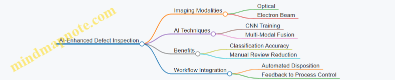
Pilot Project 3: Real-Time Film Thickness Monitoring Using Spectroscopic Ellipsometry with Digital Twins
Objective:
- To pilot real-time film thickness and refractive index monitoring during deposition using spectroscopic ellipsometry integrated with a digital twin model.
Approach:
- Deploy inline spectroscopic ellipsometers at deposition tools.
- Develop digital twin simulations of film growth dynamics.
- Use measurement data to update and refine digital twin parameters in real-time.
Outcomes:
- Enhanced prediction of film uniformity and thickness.
- Reduced process deviations by enabling proactive adjustments.
Mind Map:

Pilot Project 4: Quantum Metrology for Ultra-Precise Overlay Measurement
Objective:
- To explore quantum-enhanced measurement techniques for overlay accuracy beyond classical limits.
Approach:
- Implement pilot quantum sensors based on entangled photons for overlay measurement.
- Benchmark against diffraction-based overlay tools.
Outcomes:
- Demonstrated potential for sub-nanometer overlay precision.
- Identified challenges in environmental noise suppression.
Mind Map:

Summary
Pilot projects using next-generation metrology tools provide invaluable insights into the practical benefits and challenges of emerging technologies. By combining advanced measurement techniques with AI, digital twins, and quantum sensing, semiconductor fabs can push the boundaries of precision and process control. These pilot initiatives not only validate tool performance but also help establish best practices for integration, data management, and continuous improvement.
Additional Example Mind Map: General Pilot Project Workflow
This detailed example section illustrates how pilot projects serve as a bridge between innovation and production readiness, ensuring semiconductor manufacturing continues to meet the demands of ever-shrinking device geometries and complex architectures.
12.5 Best Practices: Preparing for Future Metrology Challenges
As semiconductor manufacturing continues to evolve rapidly, metrology engineers and process control specialists must proactively prepare for emerging challenges. This section outlines best practices to future-proof metrology strategies, supported by practical examples and mind maps to visualize key concepts.
Embrace Flexible and Modular Metrology Architectures
Future metrology tools must adapt quickly to new device architectures and materials. Designing flexible, modular systems allows easy upgrades and integration of new measurement techniques without major overhauls.
Example: A fab implemented modular scatterometry systems that could be quickly reconfigured to measure novel 3D structures like nanosheets and gate-all-around transistors, reducing downtime and accelerating process qualification.
Invest in Advanced Data Analytics and AI Integration
The volume and complexity of metrology data will increase exponentially. Leveraging AI and machine learning for anomaly detection, predictive maintenance, and process drift forecasting is essential.
Example: A process control team used machine learning models trained on historical overlay and CD metrology data to predict lithography focus shifts, enabling proactive adjustments and yield improvements.
Develop Cross-Disciplinary Collaboration and Training
Future metrology challenges span physics, materials science, data science, and manufacturing engineering. Building cross-functional teams and continuous training programs ensures comprehensive problem-solving capabilities.
Example: A fab established a “Metrology Innovation Council” comprising metrology engineers, data scientists, and process engineers who meet monthly to review emerging challenges and pilot new measurement approaches.
Prioritize Environmental Control and Equipment Stability
As device dimensions shrink, even minor environmental fluctuations can degrade measurement accuracy. Investing in ultra-stable lab environments and rigorous equipment calibration is critical.
Example: A fab upgraded its metrology labs with active vibration isolation floors and temperature-controlled enclosures, resulting in a 30% reduction in measurement noise for CD-SEM tools.
Foster Early Adoption and Pilot Testing of Emerging Technologies
Early engagement with next-generation metrology tools and techniques allows fabs to identify potential benefits and integration challenges ahead of full-scale deployment.
Example: A semiconductor manufacturer partnered with equipment vendors to pilot quantum metrology sensors for ultra-precise overlay measurement, gaining valuable insights to guide future investments.
Summary
Preparing for future metrology challenges requires a holistic approach combining flexible architectures, AI-driven analytics, cross-disciplinary collaboration, stringent environmental controls, and proactive technology adoption. By embedding these best practices into semiconductor fabs, metrology teams can maintain measurement precision and process control excellence amid rapid technological evolution.
13. Conclusion and Recommendations
13.1 Summary of Key Takeaways
Precision metrology is the backbone of semiconductor manufacturing, ensuring device performance, yield, and reliability. Throughout this blog, we explored various measurement techniques, best practices, and real-world examples that highlight the critical role of metrology in process control and innovation.
Mind Map: Core Pillars of Semiconductor Metrology
Key Takeaway 1: Measurement Technique Selection is Context-Driven
Example: For critical dimension (CD) measurement, CD-SEM offers high resolution and direct imaging, ideal for nanoscale features, whereas scatterometry provides faster, non-destructive measurements suitable for inline process control. Choosing the right tool depends on accuracy requirements, throughput, and process stage.
Key Takeaway 2: Calibration and Validation are Essential for Reliable Data
Example: Regular calibration of ellipsometers using reference wafers ensures film thickness measurements remain accurate. Cross-tool correlation, such as comparing ellipsometry with reflectometry results, helps identify drift or tool-specific biases early.
Mind Map: Best Practices for Metrology Implementation

Key Takeaway 3: Data Analytics Amplifies Metrology Value
Example: Using SPC charts to monitor overlay measurements allows early detection of process drift, enabling proactive adjustments before yield impact. Advanced predictive models can forecast equipment degradation or process excursions, reducing downtime.
Key Takeaway 4: Inline and Offline Metrology Complement Each Other
Example: Inline metrology provides rapid feedback for process control, but offline metrology offers detailed, high-accuracy analysis for root cause investigations. A hybrid approach balances throughput and precision.
Key Takeaway 5: Adaptability is Crucial for Emerging Technologies
Example: Metrology for 3D ICs requires new approaches such as 3D SEM or advanced scatterometry to measure complex topographies. Early adoption of AI-driven defect classification helps manage increased defect complexity.
Mind Map: Challenges and Solutions in Semiconductor Metrology
Final Thought:
Precision metrology is not just about measuring — it is about enabling control, insight, and continuous improvement in semiconductor manufacturing. By embracing best practices, leveraging appropriate technologies, and fostering a data-driven culture, fabs can maintain competitiveness and drive innovation in an ever-evolving landscape.
13.2 Implementing a Holistic Metrology Strategy
Implementing a holistic metrology strategy in semiconductor manufacturing is essential to ensure consistent product quality, optimize process control, and reduce yield loss. A holistic approach integrates multiple measurement techniques, data analytics, process feedback, and cross-functional collaboration to create a robust metrology ecosystem.
Key Components of a Holistic Metrology Strategy
Step 1: Integration of Measurement Techniques
A holistic strategy begins by integrating diverse metrology tools and techniques to cover all critical parameters. For example, combining CD-SEM for critical dimension measurement with scatterometry for overlay and ellipsometry for film thickness provides a comprehensive view of the wafer’s status.
Example:
-
In a leading fab, inline CD-SEM measurements are correlated with scatterometry data to detect subtle process drifts earlier than either tool alone could.
-
Cross-tool correlation helps identify discrepancies, such as a film thickness anomaly detected by ellipsometry that correlates with CD variation, enabling faster root cause identification.
Step 2: Process Control and Real-Time Feedback
Implement Statistical Process Control (SPC) across all metrology data streams to monitor process stability. Integrate real-time feedback loops to adjust process parameters dynamically.
Example:
-
A fab uses real-time overlay metrology data to adjust lithography alignment parameters on-the-fly, reducing overlay errors by 15% and improving yield.
-
Predictive analytics models trained on historical metrology data forecast process drift, allowing preemptive maintenance or process adjustments.
Step 3: Calibration, Maintenance, and Environmental Control
Regular calibration and preventive maintenance of metrology tools are critical to maintain measurement accuracy. Environmental factors such as temperature, vibration, and humidity must be controlled to minimize measurement noise.
Example:
- A fab implements a monthly calibration schedule for all CD-SEM tools and installs vibration dampening systems in metrology labs, resulting in a 10% improvement in measurement repeatability.
Step 4: Centralized Data Management and Traceability
Establish a centralized database that collects and stores all metrology data with proper traceability to wafer lots, process steps, and tool IDs. This enables comprehensive data analysis and audit trails.
Example:
- Using a Manufacturing Execution System (MES) integrated with metrology tools, a fab tracks every measurement back to the specific lot and tool, facilitating quick investigation of anomalies.
Step 5: Cross-Functional Collaboration
Encourage collaboration among metrology engineers, process control specialists, fab engineers, and data scientists to interpret data effectively and implement improvements.
Example:
- A cross-functional team reviews defect inspection data weekly to identify patterns and implement process changes, reducing defect density by 20% over six months.
Step 6: Continuous Improvement and Adaptation
Use root cause analysis on metrology deviations and yield losses to drive continuous improvement. Adapt metrology strategies as new technologies and processes emerge.
Example:
- After introducing EUV lithography, a fab updated its metrology strategy to include new overlay targets and enhanced scatterometry models, maintaining process control during technology transition.
Holistic Metrology Strategy Mind Map (Detailed)
Summary
Implementing a holistic metrology strategy requires thoughtful integration of measurement techniques, robust process control, rigorous calibration, centralized data management, and strong cross-functional collaboration. By embedding best practices and leveraging real-world examples, fabs can achieve higher measurement accuracy, tighter process control, and ultimately improved device yield and performance.
13.3 Continuous Improvement through Feedback and Innovation
Continuous improvement is a cornerstone of maintaining precision and competitiveness in semiconductor metrology. By leveraging systematic feedback loops and fostering innovation, fabs can enhance measurement accuracy, reduce variability, and accelerate process optimization.
Key Elements of Continuous Improvement in Semiconductor Metrology
Example 1: Feedback Loop Driving CD Uniformity Improvement
Scenario: A fab noticed increased variability in Critical Dimension (CD) measurements across wafers.
Approach:
- Data Collection: Inline CD-SEM measurements were continuously logged.
- Analysis: SPC charts identified a drift correlated with tool temperature fluctuations.
- Action: Process engineers adjusted tool cooling parameters and updated maintenance schedules.
- Result: CD uniformity improved by 15%, reducing wafer scrap rates.
This example highlights how timely feedback and data-driven innovation in tool operation can directly enhance metrology outcomes.
Example 2: Innovation through AI-Driven Defect Classification
Scenario: Manual defect classification was time-consuming and inconsistent.
Approach:
- Developed a machine learning model trained on historical defect images.
- Integrated AI classification into the defect review workflow.
- Continuously refined the model using feedback from defect engineers.
Result:
- Classification accuracy improved by 30%.
- Review cycle time reduced by 40%.
- Early detection of critical defects increased yield.
This demonstrates how innovation in data analytics and AI can accelerate metrology feedback loops and improve process control.
Mind Map: Continuous Improvement Feedback Cycle
Best Practices for Sustaining Continuous Improvement
- Establish Clear KPIs: Define measurable goals for metrology accuracy, throughput, and yield impact.
- Implement Real-Time Dashboards: Provide immediate visibility into metrology data and process health.
- Encourage Cross-Functional Collaboration: Break silos between metrology, process, and fab teams.
- Promote a Culture of Experimentation: Allow controlled trials of new measurement techniques and tools.
- Regularly Review and Update Processes: Use lessons learned to refine measurement protocols and training.
Final Thought
Continuous improvement through feedback and innovation is not a one-time project but an ongoing journey. By embedding these principles into the fabric of semiconductor manufacturing, fabs can maintain the highest standards of precision metrology, driving superior device performance and manufacturing excellence.
13.4 Final Practical Example: End-to-End Metrology Integration in a Leading Fab
In this section, we explore a comprehensive, real-world example of how a leading semiconductor fabrication facility (fab) successfully implemented an end-to-end metrology integration strategy. This approach harmonizes multiple metrology techniques, data analytics, and process control to achieve superior yield, precision, and throughput.
Overview of the Fab’s Metrology Integration Strategy
The fab’s goal was to create a seamless metrology ecosystem that supports all critical process steps—from wafer start to final device test—enabling real-time decision making and continuous improvement.
Key Objectives:
- Achieve sub-nanometer precision in critical dimension (CD) and overlay measurements.
- Minimize measurement cycle time without compromising accuracy.
- Integrate inline and offline metrology data into a unified analytics platform.
- Use data-driven feedback loops for process control and defect reduction.
Mind Map: End-to-End Metrology Integration Components
Step-by-Step Implementation Example
-
Measurement Technique Harmonization
- The fab standardized on CD-SEM for critical dimension measurement and scatterometry for rapid inline checks.
- Overlay metrology combined image-based and diffraction-based methods to cover different layers.
- Ellipsometry was used for film thickness monitoring.
-
Centralized Data Infrastructure
- All metrology tools were connected to a centralized Manufacturing Execution System (MES).
- Data was streamed in real-time, enabling immediate access for process engineers.
-
Advanced Analytics Integration
- SPC dashboards were developed to monitor key parameters continuously.
- Machine learning models were trained on historical defect data to classify and predict defect types.
-
Closed-Loop Process Control
- Inline metrology results triggered automatic adjustments in lithography exposure settings.
- Calibration schedules were dynamically updated based on tool drift detected via metrology data.
-
Environmental and Equipment Management
- The fab installed environmental sensors in metrology labs to track temperature and vibration.
- Maintenance was scheduled proactively to avoid measurement drift.
-
Automation and Sampling Optimization
- AI algorithms optimized sampling frequency and wafer selection to balance throughput and data quality.
Mind Map: Data Flow and Feedback Loop
Practical Examples of Impact
-
Yield Improvement: By integrating inline CD-SEM and scatterometry data, the fab reduced CD variation by 15%, directly increasing yield by 3%.
-
Defect Reduction: Machine learning-based defect classification enabled early identification of contamination sources, reducing defect density by 20%.
-
Cycle Time Reduction: Automated sampling and AI-driven scheduling cut metrology cycle times by 25%, increasing fab throughput.
-
Process Stability: Real-time SPC dashboards allowed process engineers to detect and correct lithography overlay drift within minutes instead of hours.
Lessons Learned and Best Practices
-
Cross-Functional Collaboration: Success required tight collaboration between metrology engineers, process control specialists, and fab operations.
-
Data Quality is Paramount: Rigorous data validation and cleaning ensured reliable analytics and decision making.
-
Flexibility in Tool Selection: Using complementary measurement techniques provided robustness against individual tool limitations.
-
Continuous Model Training: Machine learning models were periodically retrained with new data to maintain accuracy.
-
Environmental Control: Maintaining stable lab conditions was critical to preserving measurement precision.
This practical example demonstrates how a holistic, integrated metrology approach can transform semiconductor manufacturing, delivering measurable improvements in precision, yield, and efficiency.