Advanced CMOS Process Scaling & EUV Process Controls
1. Introduction to Advanced CMOS Process Scaling
1.1 Overview of CMOS Technology Evolution
The evolution of CMOS (Complementary Metal-Oxide-Semiconductor) technology has been a cornerstone in the advancement of semiconductor devices, enabling the exponential growth of computing power and efficiency described by Moore’s Law. This section provides a comprehensive overview of CMOS technology evolution, highlighting key milestones, scaling challenges, and practical examples to illustrate the journey from early CMOS processes to today’s advanced nodes.
Mind Map: CMOS Technology Evolution
Early CMOS Era (1970s - 1990s)
- Feature Sizes: Early CMOS devices featured large geometries, typically in the range of 10 microns down to 0.25 microns.
- Process Characteristics: Planar transistors fabricated using simple photolithography techniques.
- Example: The Intel 4004 microprocessor, introduced in 1971, was fabricated with a 10 µm process and integrated approximately 2,300 transistors.
Best Practice: Focus on robust process control and defect reduction at larger geometries to ensure yield.
Deep Submicron Era (1990s - 2000s)
- Feature Sizes: Scaling progressed to submicron dimensions, reaching 90 nm by the early 2000s.
- Technological Advances: Introduction of copper interconnects replaced aluminum to reduce resistance and improve performance.
- Example: Intel Pentium III processors used a 180 nm process node, enabling higher clock speeds and transistor density.
Best Practice: Implement advanced lithography techniques and improve interconnect materials to maintain performance scaling.
Nanometer Era (2000s - 2010s)
- Feature Sizes: Nodes scaled from 90 nm down to 22 nm.
- Innovations: Introduction of high-k dielectric materials and metal gates to reduce gate leakage.
- Strained Silicon: Used to enhance carrier mobility, improving transistor speed.
- Example: Intel’s 22 nm Tri-Gate (FinFET) transistors marked a significant shift from planar to 3D transistor architectures.
Best Practice: Integrate new materials and 3D structures carefully to balance performance gains with manufacturing complexity.
Advanced CMOS Era (2010s - Present)
- Feature Sizes: Current leading-edge nodes range from 14 nm down to 3 nm (projected).
- Transistor Architecture: FinFETs dominate, with Gate-All-Around (GAA) transistors emerging as the next step.
- Lithography: Extreme Ultraviolet (EUV) lithography is increasingly adopted to enable finer patterning.
- Example: TSMC’s 7 nm FinFET process, widely used in high-performance computing and mobile devices.
Best Practice: Employ EUV lithography and advanced process control to manage increased complexity and variability.
Example: Transition from 14 nm to 7 nm Node
- Challenge: Shrinking feature sizes increased variability and defect sensitivity.
- Solution: Adoption of EUV lithography for critical layers reduced multi-patterning complexity.
- Outcome: Improved transistor density and power efficiency enabled by tighter process controls.
Best Practice: Combine equipment upgrades with process integration strategies to ensure smooth node transitions.
Summary
The evolution of CMOS technology reflects a continuous push towards smaller, faster, and more power-efficient devices. Each era introduced new materials, architectures, and process innovations that required best practices in process control, equipment integration, and yield management. Understanding this evolution is essential for process engineers, yield engineers, and equipment engineers to navigate current challenges and prepare for future scaling.
1.2 Key Drivers for Process Scaling
Process scaling in CMOS technology is driven by multiple factors that collectively push the semiconductor industry to develop smaller, faster, and more power-efficient devices. Understanding these drivers is essential for fab process engineers, yield engineers, and equipment engineers to optimize fabrication strategies and meet market demands.
Mind Map: Key Drivers for CMOS Process Scaling
Performance Improvement
Scaling down transistor dimensions allows for faster switching speeds due to reduced channel lengths and lower parasitic capacitances. This leads to higher clock frequencies and improved overall chip performance.
Example: At the 7nm node, transistor gate lengths are significantly shorter than at 14nm, enabling processors to achieve clock speeds exceeding 3GHz with better energy efficiency. This is critical for applications like smartphones and gaming consoles where performance per watt is a key metric.
Power Efficiency
Smaller transistors consume less power, both dynamic and static. Dynamic power scales with capacitance and voltage squared, so reducing transistor size and operating voltage directly lowers power consumption. Additionally, advanced materials and device architectures help reduce leakage currents.
Example: In IoT devices, battery life is paramount. By scaling CMOS processes to 5nm and below, manufacturers reduce operating voltages from 1.0V to around 0.7V, cutting dynamic power consumption by nearly 50%, enabling longer device uptime.
Cost Reduction
Although advanced nodes require significant R&D investment, scaling ultimately reduces cost per function by increasing the number of dies per wafer and improving yield through refined process controls.
Example: Moving from 28nm to 14nm technology doubles the transistor density, allowing twice as many chips per wafer. Despite higher initial tool costs, the cost per chip decreases, making advanced nodes economically viable for high-volume production.
Functional Integration
Process scaling enables integration of more functions on a single chip, reducing the need for multiple discrete components and improving system performance and reliability.
Example: Modern SoCs integrate CPU cores, GPUs, AI accelerators, and analog interfaces on a single die at 7nm and below, reducing board space and power consumption in smartphones.
Market Demand
The proliferation of mobile devices, AI workloads, automotive electronics, and IoT sensors drives the need for smaller, faster, and more efficient chips.
Example: AI accelerators require high transistor density and low latency, pushing fabs to adopt 5nm and EUV lithography to meet these performance demands.
Integrated Example: Balancing Drivers in a 5nm Mobile SoC
- Performance: Achieved 15% higher clock speeds compared to 7nm.
- Power: Reduced operating voltage by 0.2V, cutting dynamic power by 35%.
- Cost: Despite higher process complexity, cost per transistor decreased by 25%.
- Integration: Included AI and 5G modem on the same die.
This example demonstrates how multiple drivers interplay to justify aggressive process scaling.
Summary
Process scaling is propelled by the need to improve performance, reduce power consumption, lower costs, integrate more functionality, and satisfy evolving market demands. Each driver influences process development priorities and equipment requirements, making a holistic understanding crucial for successful CMOS fabrication.
1.3 Challenges in Sub-10nm CMOS Nodes
As CMOS technology scales below the 10nm node, semiconductor fabrication faces a multitude of complex challenges that impact device performance, manufacturability, and yield. This section explores these challenges in detail, supported by mind maps and practical examples to aid understanding.
Key Challenges Overview
Lithography Limitations
At sub-10nm nodes, traditional optical lithography approaches reach their physical limits. Even with EUV lithography, challenges persist:
-
Resolution Limits: The wavelength of EUV (13.5 nm) allows finer patterning, but stochastic effects such as photon shot noise lead to line width variability.
-
Overlay Accuracy: Precise alignment between multiple patterning steps is critical; any misalignment can cause device failure.
-
Stochastic Defects: Random variations in resist exposure and development cause pattern roughness and missing features.
Example: In a 7nm node process, stochastic defects caused by photon shot noise led to a 5% increase in line edge roughness (LER), which directly impacted transistor threshold voltage variability.
Device Variability
As device dimensions shrink, variability becomes a dominant concern:
-
Random Dopant Fluctuations (RDF): At nanoscale, the number of dopant atoms per device is very small, causing threshold voltage variations.
-
Line Edge Roughness (LER): Variations in the edge of patterned lines cause electrical performance fluctuations.
-
Process-Induced Variations: Variations in etch, deposition, and annealing steps introduce device-to-device differences.
Example: In a 5nm FinFET device, RDF contributed to a threshold voltage variation of ±20mV, which affected the overall circuit timing margin.
Material and Process Integration
Scaling below 10nm requires advanced materials and complex integration schemes:
-
High-k/Metal Gate Scaling: Thinner gate dielectrics increase leakage; integrating new materials without degrading mobility is challenging.
-
Contact Resistance: Shrinking contact areas increase resistance, impacting drive current.
-
Strain Engineering: Applying strain to improve carrier mobility becomes more difficult with smaller geometries.
Example: At 7nm, integrating a new high-k dielectric with a metal gate stack reduced gate leakage by 30%, but required process adjustments to maintain uniformity.
Power and Performance Trade-offs
Sub-10nm nodes face increased short channel effects and leakage currents:
-
Short Channel Effects: Reduced channel length leads to drain-induced barrier lowering and threshold voltage roll-off.
-
Leakage Currents: Increased leakage impacts static power consumption.
-
Variability Impact: Device variability exacerbates power-performance trade-offs.
Example: In a 5nm node SRAM cell, leakage current increased by 40%, necessitating new power gating techniques to maintain battery life.
Yield and Defect Control
Yield challenges intensify as feature sizes shrink:
-
Defect Density Increase: Smaller features are more sensitive to particulate and pattern defects.
-
Stochastic Defects in EUV: Random photon and electron interactions cause missing or bridging features.
-
Process Window Shrinkage: Narrower process windows increase sensitivity to process variations.
Example: A foundry reported a 15% yield drop when transitioning to 7nm EUV due to increased stochastic defects, which was mitigated by optimized resist formulations and dose control.
Summary
Sub-10nm CMOS nodes present a complex interplay of lithographic, material, device, and yield challenges. Understanding these challenges through mind maps and real-world examples helps process engineers and yield engineers develop targeted solutions to push scaling forward while maintaining performance and yield.
1.4 Best Practices: Balancing Performance, Power, and Area with Real-World Examples
Balancing Performance, Power, and Area (PPA) is a critical challenge in advanced CMOS process scaling. Achieving an optimal trade-off among these three parameters ensures competitive chip designs that meet market demands for speed, energy efficiency, and cost-effectiveness.
Key Concepts in PPA Balancing
- Performance: Measured by speed (frequency), throughput, and latency.
- Power: Includes dynamic power (switching) and static/leakage power.
- Area: The silicon real estate consumed by the design, impacting cost and yield.
Mind Map: Core Elements of PPA Balancing
Best Practices for Balancing PPA
-
Device Engineering Optimization
- Utilize FinFET or GAAFET architectures to improve electrostatic control, reducing leakage power while enabling high performance.
- Example: At 7nm node, Intel’s introduction of FinFETs reduced leakage by ~30% compared to planar transistors, enabling higher frequency operation without excessive power increase.
-
Threshold Voltage (Vth) Tuning
- Employ multiple threshold voltage devices within the same design. High-Vth devices reduce leakage in non-critical paths; low-Vth devices boost speed in critical paths.
- Example: TSMC 5nm process uses multi-Vth libraries, achieving up to 15% power savings without performance loss.
-
Power Gating and Dynamic Voltage/Frequency Scaling (DVFS)
- Integrate power gating to shut off idle blocks, reducing leakage power.
- Use DVFS to dynamically adjust voltage and frequency based on workload.
- Example: Qualcomm Snapdragon processors implement aggressive power gating and DVFS, extending battery life while maintaining peak performance.
-
Layout and Design for Manufacturability (DFM)
- Optimize cell layouts to minimize area without compromising signal integrity.
- Use EUV lithography to reduce multi-patterning complexity, improving area efficiency.
- Example: Samsung’s 5nm node leveraged EUV to reduce metal layer pitches, shrinking area by ~10% compared to 7nm.
-
Process Integration and Material Innovations
- Incorporate high-k metal gate stacks to reduce gate leakage.
- Use strain engineering to boost carrier mobility, enhancing performance without increasing power.
- Example: IBM’s use of SiGe stressors in 7nm FinFETs improved drive current by 10%, enabling better PPA balance.
Mind Map: Techniques to Improve PPA
Real-World Example: Balancing PPA in a 7nm Mobile SoC Design
- Challenge: Achieve high CPU frequency for gaming performance while maintaining battery life and minimizing chip size.
- Approach:
- Use low-Vth transistors in CPU critical paths for speed.
- Apply high-Vth devices in background logic to reduce leakage.
- Implement aggressive power gating on unused blocks.
- Employ EUV lithography to reduce metal pitch and shrink area.
- Outcome:
- 20% frequency improvement over previous generation.
- 25% reduction in leakage power during idle states.
- 8% die size reduction, lowering manufacturing cost.
Summary
Balancing performance, power, and area requires a holistic approach that spans device engineering, circuit design, process innovation, and layout optimization. Leveraging advanced transistor architectures, multi-Vth libraries, power management techniques, and EUV-enabled process improvements enables semiconductor fabs and process engineers to meet the stringent demands of modern CMOS scaling.
By integrating these best practices with real-world examples, engineers can systematically navigate the PPA trade-offs to deliver competitive and efficient semiconductor products.
1.5 Case Study: Transition from 14nm to 7nm Node
The transition from the 14nm to the 7nm CMOS node represents one of the most significant leaps in semiconductor fabrication technology. This case study explores the technical challenges, process innovations, and best practices that enabled this scaling, with practical examples and mind maps to clarify complex concepts.
Overview of the Transition
- Scaling Goals: Achieve higher transistor density, improved performance, and reduced power consumption.
- Key Challenges: Lithography limitations, increased variability, new materials integration, and tighter process controls.
Mind Map: Key Areas in 14nm to 7nm Transition
Lithography Innovations
Best Practice: Introduction of Extreme Ultraviolet (EUV) lithography to reduce reliance on complex multi-patterning.
- Example: At 14nm, quadruple patterning was common to achieve required pitches, increasing complexity and cost.
- At 7nm, EUV enabled single patterning for critical layers, simplifying the process flow and improving overlay accuracy.
Mind Map: Lithography Evolution
Device Architecture Enhancements
Best Practice: Optimization of FinFET structures for improved electrostatics and performance.
- Example: Increasing fin height and fin density at 7nm to boost drive current without increasing footprint.
- Exploration of Gate-All-Around (GAA) transistors began as a future-proofing measure.
Mind Map: Device Architecture Changes
Materials and Process Integration
Best Practice: Refinement of high-k metal gate stacks to reduce variability and improve threshold voltage control.
- Example: Introduction of new metal gate alloys and improved deposition techniques to enhance uniformity.
- Use of advanced etch and deposition processes to maintain tight CD control.
Mind Map: Materials & Integration
Process Control and Metrology
Best Practice: Implementing in-line metrology and advanced process control (APC) to monitor critical dimensions and reduce variability.
- Example: Use of CD-SEM and scatterometry to detect line edge roughness and fin height variations in real-time.
- Statistical Process Control (SPC) charts were employed to track process drift and trigger corrective actions.
Mind Map: Process Control
Yield Management and Defect Control
Best Practice: Focused reduction of stochastic defects inherent in EUV lithography through process optimization and defect inspection.
- Example: Adjusting resist formulations and exposure parameters to minimize line breaks and bridging.
- Deployment of machine learning algorithms in defect classification to accelerate root cause analysis.
Mind Map: Yield Management
Summary of Lessons Learned
- Early adoption of EUV lithography was critical to simplifying patterning complexity.
- Tight integration between device design and process engineering ensured performance gains without sacrificing yield.
- Advanced metrology and APC systems are indispensable for maintaining process stability at 7nm.
- Cross-disciplinary collaboration among fab process engineers, yield engineers, and equipment engineers accelerated problem-solving.
This case study underscores the importance of holistic process innovation and control in successfully scaling CMOS technology nodes, providing a blueprint for future transitions.
2. Fundamentals of EUV Lithography in CMOS Scaling
2.1 EUV Lithography Basics and Equipment Overview
EUV (Extreme Ultraviolet) lithography is a cutting-edge technology enabling semiconductor fabrication at advanced nodes, typically sub-7nm. It uses light with a wavelength of 13.5 nm, significantly shorter than traditional deep ultraviolet (DUV) lithography (193 nm), allowing finer patterning and higher resolution.
What is EUV Lithography?
EUV lithography employs extreme ultraviolet light to transfer circuit patterns onto silicon wafers. The shorter wavelength allows printing of smaller features with fewer patterning steps.
Key components:
- EUV light source
- Reflective optics (mirrors)
- Photomask (reticle)
- Photoresist-coated wafer
Mind Map: EUV Lithography Fundamentals
EUV Equipment Overview
-
EUV Source: Generates EUV photons by firing high-energy lasers at tin droplets, creating plasma that emits 13.5 nm wavelength light.
-
Illumination Optics: Collects and shapes the EUV light, directing it towards the mask.
-
Mask Stage: Holds the reflective photomask that contains the circuit pattern.
-
Projection Optics: A series of multilayer mirrors project the mask pattern onto the wafer.
-
Wafer Stage: Precisely moves the wafer under the projection optics for patterning.
-
Control Systems: Manage alignment, focus, dose, and overlay accuracy.
Mind Map: EUV Equipment Components
Example: EUV Source Power and Throughput
A typical EUV source delivers around 250 watts of EUV power, enabling wafer throughput of approximately 125 wafers per hour. Increasing source power directly improves throughput but requires advanced cooling and debris mitigation strategies.
Best Practice: Regular maintenance of the tin droplet injector and laser alignment ensures stable EUV power output, minimizing downtime.
Example: Reflective Mask Challenges
Unlike traditional masks, EUV masks are reflective, requiring multilayer coatings and absorber patterns. Defects on the mask surface can print onto wafers, so mask inspection and repair are critical.
Best Practice: Implement mask blank inspection and repair cycles before mask fabrication to reduce defect density.
Summary
EUV lithography represents a paradigm shift in semiconductor patterning, leveraging a complex system of source generation, reflective optics, and precision stages. Understanding the fundamentals and equipment architecture is essential for process engineers, yield engineers, and equipment engineers to optimize and control advanced CMOS fabrication.
For further reading, see:
- “EUV Lithography: Lithography Gets Extreme” by Chris A. Mack
- ASML EUV Scanner Technical Whitepapers
2.2 EUV Source Power and Stability: Best Practices for Maximizing Throughput
Extreme Ultraviolet (EUV) lithography is a cornerstone technology for advanced CMOS process scaling, enabling patterning at sub-7nm nodes. The EUV source power and its stability directly impact wafer throughput, pattern fidelity, and overall process yield. This section delves into best practices for optimizing EUV source power and stability, supported by practical examples and mind maps to aid understanding.
Understanding EUV Source Power and Stability
- EUV Source Power: The intensity of EUV light generated, typically measured in watts (W). Higher source power allows faster exposure times, increasing wafer throughput.
- Source Stability: The consistency of EUV power output over time. Fluctuations can cause critical dimension (CD) variations and defects.
Maintaining a high and stable EUV source power is essential to balance throughput and process control.
Best Practices for Maximizing EUV Source Power and Stability
Optimizing Laser-Produced Plasma (LPP) Conditions
- Droplet Generation Control: Precise timing and size control of tin droplets that serve as EUV targets.
- Laser Pulse Energy and Focus: Adjusting laser parameters to maximize plasma efficiency.
- Example: At a leading fab, tuning laser pulse energy by 5% improved source power by 10%, reducing exposure time per wafer by 8%.
Real-Time Source Monitoring and Feedback
- Power Sensors: Use of in-situ power sensors to monitor EUV intensity.
- Feedback Loops: Automated adjustments to laser parameters based on sensor data.
- Example: Implementing closed-loop control reduced power fluctuations from ±5% to ±1.5%, enhancing CD uniformity.
Preventive Maintenance and Contamination Control
- Tin Debris Mitigation: Regular cleaning of collector mirrors and use of debris mitigation technologies.
- Scheduled Maintenance: Proactive replacement of consumables to avoid sudden power drops.
- Example: A fab reduced unplanned downtime by 30% through a strict debris management protocol.
Environmental Stability
- Temperature and Humidity Control: Maintaining stable environmental conditions to prevent source instability.
- Vibration Isolation: Minimizing mechanical vibrations that affect laser and droplet alignment.
Source Power Scaling Strategies
- Incremental Power Increases: Gradually scaling source power to avoid equipment stress.
- Parallel Source Operation: Using multiple sources or scanners to balance load and increase throughput.
Mind Map: EUV Source Power Optimization
Mind Map: Impact of Source Power Stability on Throughput and Yield
Practical Example: Improving Throughput via Source Power Stability
Scenario: A semiconductor fab experienced throughput bottlenecks due to EUV source power fluctuations causing frequent exposure retries.
Actions Taken:
- Implemented enhanced droplet generator calibration to improve tin droplet uniformity.
- Installed advanced in-situ power sensors with real-time feedback to laser control.
- Adopted a rigorous debris mitigation schedule including mirror cleaning every 48 hours.
Results:
- Source power stability improved from ±4% variance to ±1%.
- Exposure time per wafer decreased by 12%, increasing wafers per hour by 15%.
- Yield improved by 3% due to reduced CD variability.
Summary
Maximizing EUV source power and maintaining its stability are critical for achieving high throughput and yield in advanced CMOS fabrication. Best practices include optimizing plasma generation, real-time monitoring with feedback control, rigorous maintenance, and environmental stabilization. By implementing these strategies, fabs can significantly enhance process performance and equipment reliability.
For process engineers, yield engineers, and equipment engineers, understanding and applying these best practices ensures the EUV lithography step supports the aggressive scaling roadmap of modern semiconductor manufacturing.
2.3 Mask Design and Defect Management in EUV
EUV lithography has revolutionized semiconductor fabrication by enabling smaller feature sizes and higher pattern fidelity. However, the mask design and defect management in EUV present unique challenges compared to traditional optical lithography due to the nature of EUV light and mask construction.
Overview of EUV Mask Structure
EUV masks differ fundamentally from conventional photomasks:
- Reflective mask: EUV masks are reflective, not transmissive, composed of a multilayer mirror (typically Mo/Si) topped with an absorber pattern.
- Multilayer stack: The multilayer stack reflects EUV light at ~13.5 nm wavelength.
- Absorber layer: Defines the pattern by absorbing EUV light in specific areas.
Mind Map: EUV Mask Structure
Mask Design Considerations
-
Pattern Fidelity and Resolution:
- Design must compensate for mask 3D effects (shadowing, phase shift).
- Use of Optical Proximity Correction (OPC) tailored for EUV.
-
Mask Error Enhancement Factor (MEEF):
- EUV masks have higher MEEF due to reflective nature.
- Design strategies to minimize MEEF impact include pattern smoothing and biasing.
-
Defect Tolerance:
- Defects on the multilayer or absorber can print on wafer.
- Design must consider defect avoidance or repair strategies.
-
Mask Complexity and Write Time:
- High-resolution patterns increase e-beam write time.
- Hierarchical design and fracturing strategies optimize write efficiency.
Mind Map: Mask Design Considerations
Defect Types and Sources in EUV Masks
- Multilayer Defects: Particles or pits in the Mo/Si layers causing reflectivity anomalies.
- Absorber Defects: Missing or extra absorber material causing pattern distortions.
- Substrate Defects: Surface roughness or contamination affecting multilayer deposition.
Example: A pit defect in the multilayer stack can cause a bright spot on the wafer, leading to a critical dimension (CD) variation or bridging.
Defect Detection and Inspection Techniques
- Mask Blank Inspection: Detects defects before absorber patterning.
- Post-Patterning Inspection: Identifies defects after absorber deposition.
- Actinic Inspection: Uses EUV light to detect defects under actual exposure conditions.
- Aerial Image Metrology: Simulates wafer printability of mask defects.
Mind Map: Defect Inspection Techniques
Defect Mitigation and Repair Strategies
-
Defect Avoidance:
- Select defect-free mask blanks.
- Optimize multilayer deposition processes.
-
Defect Repair:
- Focused Ion Beam (FIB) milling to remove absorber defects.
- Atomic Layer Deposition (ALD) to fill pits in multilayer.
-
Design for Manufacturability (DfM):
- Incorporate redundancy or pattern adjustments to tolerate defects.
-
Mask Cleaning:
- Regular cleaning to remove contamination without damaging multilayer.
Example: Repairing a multilayer pit defect by ALD filling restored reflectivity and eliminated a bright spot on wafer prints.
Best Practices with Examples
-
Example 1: OPC Tailoring for EUV Masks
- Implemented 3D OPC corrections considering mask shadowing.
- Resulted in 15% improvement in CD uniformity across wafer.
-
Example 2: Actinic Inspection Integration
- Introduced actinic inspection tool in mask qualification.
- Early detection of print-impacting defects reduced scrap rate by 20%.
-
Example 3: Defect Repair Workflow
- Combined FIB and ALD repair steps.
- Enabled reuse of masks previously deemed non-repairable, saving $500K per mask.
Summary
Mask design and defect management in EUV lithography require a holistic approach integrating advanced design techniques, precise inspection, and effective repair strategies. By understanding the unique challenges of EUV masks and applying best practices, fab process engineers can significantly improve yield and device performance.
For further reading, consider exploring:
- EUV Mask Blank Defectivity Reports
- OPC Algorithms for EUV Lithography
- Advances in Actinic Mask Inspection Technologies
2.4 Resist Materials and Sensitivity Optimization with Practical Examples
Introduction
Resist materials play a critical role in EUV lithography, directly impacting resolution, line edge roughness (LER), sensitivity, and ultimately yield. Sensitivity optimization balances dose requirements with resist performance, enabling high throughput and defect control.
Overview of Resist Materials for EUV Lithography
- Chemically Amplified Resists (CARs): Most common, rely on acid catalysis for post-exposure reactions.
- Non-Chemically Amplified Resists: Offer potentially lower LER but often lower sensitivity.
- Metal-oxide Resists: Emerging materials with high resolution and sensitivity.
Mind Map: Resist Material Types
Key Parameters Affecting Resist Sensitivity
- Absorption Coefficient: EUV photons are absorbed in the resist; higher absorption increases sensitivity but may degrade resolution.
- Photoacid Generator (PAG) Efficiency: Determines how effectively photons generate acid to catalyze reactions.
- Resist Film Thickness: Thicker films may require higher doses.
- Post-Exposure Bake (PEB) Conditions: Affect acid diffusion and reaction kinetics.
Mind Map: Factors Influencing Resist Sensitivity
Sensitivity Optimization Strategies
Material Engineering
- Tailoring polymer backbone and PAG concentration to optimize acid generation and diffusion.
- Example: Increasing PAG concentration improved sensitivity by 15% but required tighter control on LER.
Process Parameter Tuning
- Adjusting PEB temperature and time to balance acid diffusion and minimize LER.
- Example: Lowering PEB temperature from 120°C to 110°C reduced acid diffusion length, improving pattern fidelity.
Resist Thickness Control
- Thinner resist films reduce dose requirements but may compromise etch resistance.
- Example: Reducing resist thickness from 40nm to 30nm decreased dose by 20%, enabling higher throughput.
Mind Map: Sensitivity Optimization Techniques
Practical Examples
Example 1: Enhancing Sensitivity via PAG Modification
- Context: A fab experienced throughput bottlenecks due to high dose requirements (~30 mJ/cm²).
- Action: Modified PAG chemistry to increase quantum efficiency.
- Result: Dose reduced to 25 mJ/cm², throughput improved by 20% with marginal LER increase.
Example 2: PEB Optimization to Minimize LER
- Context: Excessive acid diffusion causing pattern blurring.
- Action: Reduced PEB temperature and shortened bake time.
- Result: LER improved by 10%, dose remained stable.
Example 3: Resist Thickness Adjustment for Dose Reduction
- Context: High dose led to slow wafer processing.
- Action: Thinned resist from 40 nm to 30 nm.
- Result: Dose requirement dropped by 20%, but etch resistance required compensatory hard mask tuning.
Balancing Sensitivity with Other Resist Performance Metrics
- Resolution: Higher sensitivity resists sometimes compromise resolution.
- Line Edge Roughness (LER): Increased acid diffusion can worsen LER.
- Etch Resistance: Thinner or more sensitive resists may degrade etch durability.
Mind Map: Resist Performance Trade-offs
Summary
Optimizing resist materials and sensitivity in EUV lithography is a multi-dimensional challenge involving chemistry, process engineering, and equipment capabilities. Practical tuning of PAG chemistry, PEB conditions, and resist thickness can significantly improve throughput and pattern fidelity. Understanding trade-offs ensures balanced performance for advanced CMOS scaling.
References & Further Reading
- “EUV Lithography Resist Materials and Processes,” Journal of Micro/Nanolithography, MEMS, and MOEMS, 2022.
- “Optimization of Chemically Amplified Resists for EUV Lithography,” SPIE Proceedings, 2021.
- Industry case studies from leading foundries on resist sensitivity improvements.
2.5 Case Study: Implementing EUV in High-Volume Manufacturing
Introduction
The transition to Extreme Ultraviolet (EUV) lithography has been a pivotal milestone for semiconductor fabs aiming to scale CMOS technology nodes beyond 7nm. This case study explores the practical implementation of EUV lithography in a high-volume manufacturing (HVM) environment, highlighting key challenges, best practices, and solutions that enabled successful integration.
Background
A leading semiconductor foundry initiated EUV adoption to address the increasing complexity and cost of multi-patterning techniques at sub-7nm nodes. The goal was to leverage EUV’s single-exposure capability to simplify process flows, improve overlay accuracy, and enhance throughput.
Key Implementation Phases
-
Phase 1: Pilot Line Evaluation
- Equipment qualification and baseline performance assessment
- Resist and mask material testing
- Process recipe development
-
Phase 2: Process Integration and Optimization
- Integration of EUV steps into existing process flows
- Optimization of critical dimension (CD) uniformity and line edge roughness (LER)
- Defectivity reduction strategies
-
Phase 3: Ramp to High-Volume Manufacturing
- Throughput scaling and tool uptime improvement
- In-line metrology and process control implementation
- Yield monitoring and feedback loops
Mind Map: EUV Implementation Workflow
Best Practices and Examples
Equipment Qualification and Maintenance
- Best Practice: Establish rigorous source power and optics cleanliness monitoring protocols.
- Example: The fab implemented daily EUV source power calibration and weekly mirror cleaning schedules, reducing unexpected downtime by 30%.
Resist and Mask Optimization
- Best Practice: Use high-sensitivity resists with optimized post-exposure bake (PEB) parameters to balance resolution and defectivity.
- Example: By adjusting PEB temperature profiles, the fab reduced stochastic defects by 15%, improving yield.
Process Integration
- Best Practice: Integrate EUV lithography steps early in the process flow to minimize overlay errors.
- Example: The fab shifted critical patterning layers to EUV exposure, achieving overlay accuracy within 3nm, surpassing previous multi-patterning methods.
Defectivity Control
- Best Practice: Implement in-line mask inspection and wafer defect monitoring.
- Example: Real-time defect data enabled rapid identification of mask contamination sources, leading to a 20% reduction in defect density.
Throughput Enhancement
- Best Practice: Optimize tool uptime through predictive maintenance and operator training.
- Example: Predictive analytics reduced unplanned tool downtime by 25%, increasing wafer throughput.
Yield Monitoring and Feedback
- Best Practice: Deploy advanced metrology tools and statistical process control (SPC) for real-time feedback.
- Example: Continuous CD uniformity monitoring allowed immediate process adjustments, improving yield by 10%.
Mind Map: Yield Improvement via EUV Process Controls
Summary
The successful implementation of EUV lithography in high-volume manufacturing requires a holistic approach encompassing equipment readiness, process development, defectivity control, throughput optimization, and yield management. By adopting best practices such as rigorous equipment maintenance, resist and mask optimization, and advanced process controls, fabs can harness EUV’s potential to drive next-generation CMOS scaling effectively.
This case study demonstrates that integrating EUV lithography is not just a technological upgrade but a comprehensive transformation involving cross-disciplinary collaboration and continuous improvement.
References & Further Reading
- EUV Lithography: Principles, Technology, and Applications, SPIE Press
- SEMATECH EUV Source and Resist Studies
- Industry Whitepapers on EUV Implementation in HVM
3. Process Integration Challenges in Advanced CMOS Nodes
3.1 Critical Dimension Control and Uniformity
Critical Dimension (CD) control and uniformity are paramount in advanced CMOS process nodes, especially as feature sizes shrink below 10nm. Precise CD control ensures device performance, yield, and reliability, while uniformity across the wafer and between wafers guarantees consistent electrical characteristics.
What is Critical Dimension (CD)?
- The smallest feature size in a pattern, such as gate length, line width, or space.
- Directly impacts transistor speed, leakage, and power consumption.
Why is CD Control Challenging in Advanced Nodes?
- Increased pattern complexity and density.
- Limitations of lithography resolution and process variability.
- Stochastic effects in EUV lithography causing line edge roughness (LER) and stochastic defects.
Mind Map: Factors Affecting CD Control and Uniformity
Best Practices for CD Control & Uniformity
-
Optimized Lithography Process
- Use of advanced dose and focus matrix (DFM) experiments to find optimal exposure parameters.
- Example: At a 7nm node fab, adjusting EUV dose by ±5% reduced CD variation by 15% across the wafer.
-
Mask Quality and Management
- Regular inspection and cleaning of EUV masks to minimize defects.
- Example: Implementing pellicles on EUV masks reduced particle-induced CD variation by 10%.
-
Etch Process Tuning
- Fine-tuning etch chemistry and plasma conditions to maintain uniform etch rates.
- Example: Switching to a multi-step etch process improved CD uniformity from 4nm to 2nm across the wafer.
-
Advanced Metrology Integration
- Deploying high-resolution CD-SEM and scatterometry tools for real-time monitoring.
- Example: Using in-line scatterometry feedback enabled early detection of CD drift, preventing yield loss.
-
Statistical Process Control (SPC)
- Continuous monitoring of CD data and implementing control charts to detect trends.
- Example: SPC identified a tool drift causing CD shifts, enabling timely maintenance and restoring uniformity.
Mind Map: CD Control Workflow
Example: Implementing CD Uniformity Improvement at a 5nm Node
Scenario: A fab observed increased CD variation (>3nm) on gate patterns after EUV exposure and etch steps.
Actions Taken:
- Conducted a lithography dose-focus matrix to identify optimal exposure conditions.
- Enhanced mask inspection frequency and introduced pellicle usage.
- Tuned etch plasma parameters to reduce microloading effects.
- Integrated in-line CD-SEM measurements with SPC to monitor trends.
Results:
- CD variation reduced to <1.5nm across the wafer.
- Yield improved by 8% due to tighter CD control.
Summary
Maintaining tight CD control and uniformity is a multi-disciplinary effort involving lithography, etch, metrology, and process control. By combining optimized process parameters, advanced metrology, and continuous monitoring, fabs can achieve the precision required for advanced CMOS nodes. Real-world examples demonstrate that even small adjustments in dose, mask management, and etch conditions can significantly improve CD uniformity and overall device yield.
3.2 Etch Process Optimization for EUV Patterns
Introduction
Etching is a critical step in semiconductor fabrication, especially when dealing with EUV (Extreme Ultraviolet) lithography patterns. The shift to EUV introduces unique challenges due to the finer feature sizes, increased pattern complexity, and sensitivity to process variations. Optimizing the etch process ensures high fidelity pattern transfer, minimal damage, and improved device performance.
Key Challenges in Etching EUV Patterns
- Feature Size Reduction: Sub-7nm features require ultra-precise etch control.
- Pattern Complexity: EUV enables complex 3D structures that demand anisotropic and selective etching.
- Line Edge Roughness (LER): Minimizing roughness is critical to maintain electrical integrity.
- Etch Selectivity: Balancing etch rates between different materials (e.g., resist, hard mask, substrate).
- Etch Uniformity: Across the wafer and from batch to batch.
Mind Map: Etch Process Optimization Factors
Best Practices and Examples
Gas Chemistry Tuning
- Practice: Optimize gas mixtures (e.g., SF6, C4F8, O2) to achieve high anisotropy and selectivity.
- Example: At a 5nm node, adjusting the ratio of C4F8 to SF6 reduced sidewall roughness by 15%, improving device reliability.
RF Power and Pressure Control
- Practice: Fine-tune RF power to balance ion energy and density, controlling etch rate and damage.
- Example: Lowering RF power from 300W to 250W in a fluorocarbon plasma reduced substrate damage while maintaining etch rate.
Temperature Management
- Practice: Maintain wafer temperature to prevent polymer buildup or excessive etch rates.
- Example: Implementing a 20°C chuck temperature stabilized etch uniformity across the wafer, reducing CD variation by 10%.
Addressing Microloading and Aspect Ratio Dependent Etching (ARDE)
- Practice: Use pulsed plasma or tailored gas flows to mitigate microloading.
- Example: Pulsed plasma etching reduced ARDE effects in dense EUV patterns, resulting in uniform trench depths.
End-Point Detection and In-Situ Monitoring
- Practice: Employ optical emission spectroscopy (OES) and laser interferometry for real-time etch endpoint detection.
- Example: Real-time OES monitoring prevented over-etching in finFET structures, improving yield by 8%.
Mind Map: Example Workflow for Etch Optimization
Real-World Example: Optimizing Etch for EUV-Patterned FinFETs
At a leading foundry, engineers faced challenges with etching 5nm node FinFET fins patterned by EUV. Initial processes showed excessive sidewall roughness and CD variation.
-
Approach:
- Conducted a DOE varying C4F8/SF6 ratios and RF power.
- Implemented pulsed plasma etching to reduce ion bombardment damage.
- Used in-situ OES for endpoint detection.
-
Outcome:
- Sidewall roughness decreased by 20%.
- CD uniformity improved by 12%.
- Yield improved by 7% due to reduced defects.
Summary
Optimizing etch processes for EUV patterns requires a holistic approach encompassing chemistry, equipment parameters, pattern considerations, and real-time monitoring. By applying best practices such as gas chemistry tuning, RF power control, and advanced endpoint detection, process engineers can achieve high fidelity pattern transfer essential for advanced CMOS scaling.
References & Further Reading
- “Plasma Etching for Semiconductor Fabrication,” Journal of Vacuum Science & Technology
- ASML EUV Lithography Whitepapers
- SEMATECH Reports on Etch Process Control
3.3 Deposition Techniques for High-k/Metal Gate Stacks
In advanced CMOS process nodes, the integration of high-k dielectrics and metal gate stacks is critical to achieving improved transistor performance, reduced leakage currents, and enhanced scalability. This section delves into the deposition techniques used for high-k/metal gate stacks, highlighting best practices and providing practical examples to aid fab process engineers, yield engineers, and equipment engineers.
Overview of High-k/Metal Gate Stack Deposition
The high-k/metal gate stack typically consists of a high-k dielectric layer (such as HfO2, ZrO2) deposited over the silicon channel, followed by one or more metal gate layers (e.g., TiN, TaN, W). The deposition process must ensure excellent film uniformity, low defect density, and precise thickness control to maintain device performance and yield.
Common Deposition Techniques
-
Atomic Layer Deposition (ALD)
- Provides atomic-scale thickness control and excellent conformality.
- Ideal for depositing ultra-thin high-k dielectric films.
- Example: Deposition of 1.5 nm HfO2 layer with ±0.1 nm uniformity across 300 mm wafers.
-
Physical Vapor Deposition (PVD)
- Commonly used for metal gate electrode layers.
- Offers good step coverage but may have limitations in complex 3D structures.
- Example: TiN metal gate deposition with controlled resistivity and stress.
-
Chemical Vapor Deposition (CVD)
- Used for some metal layers and barrier films.
- Provides good conformality and throughput.
- Example: Deposition of TaN barrier layer to prevent metal diffusion.
Mind Map: Deposition Techniques for High-k/Metal Gate Stacks
Best Practices in Deposition
-
Pre-Deposition Surface Preparation
- Ensure native oxide removal and surface passivation.
- Example: Use of in-situ plasma cleaning before ALD to improve adhesion and reduce interface traps.
-
ALD Process Optimization
- Optimize precursor pulse times and purge cycles to avoid CVD-like growth.
- Example: Adjusting Hf precursor pulse to minimize carbon contamination.
-
Temperature Control
- Maintain deposition temperature within tight limits to ensure film quality.
- Example: ALD HfO2 deposition at 250°C ± 5°C for optimal crystallinity.
-
Thickness Uniformity Monitoring
- Use in-situ ellipsometry or reflectometry to monitor film thickness.
- Example: Real-time feedback enables correction of non-uniformity across wafer.
-
Post-Deposition Annealing
- Perform rapid thermal annealing (RTA) to improve film density and electrical properties.
- Example: RTA at 600°C for 30 seconds to reduce interface trap density.
Example: ALD of HfO2 High-k Dielectric Layer
- Objective: Deposit a 1.5 nm HfO2 layer with uniform thickness and low defect density.
- Process:
- Substrate cleaning with HF dip to remove native oxide.
- In-situ plasma treatment for surface activation.
- ALD cycles using HfCl4 and H2O precursors at 250°C.
- Pulse and purge times optimized to prevent CVD growth.
- Outcome: Achieved ±0.1 nm thickness uniformity and low leakage current in MOS capacitors.
Example: PVD TiN Metal Gate Deposition
- Objective: Deposit a TiN metal gate layer with controlled resistivity and stress.
- Process:
- PVD sputtering with Ti target in N2/Ar atmosphere.
- Control of chamber pressure and power to tune film properties.
- Use of substrate bias to improve film density.
- Outcome: TiN film with resistivity ~200 µΩ·cm and tensile stress optimized to minimize gate deformation.
Mind Map: Best Practices for High-k/Metal Gate Deposition
Summary
Mastering deposition techniques for high-k/metal gate stacks is essential for successful CMOS scaling. ALD remains the gold standard for high-k dielectric layers due to its atomic-level control, while PVD and CVD complement metal gate and barrier layer depositions. Implementing best practices such as rigorous surface preparation, precise process control, and real-time monitoring ensures high-quality films that meet the stringent requirements of advanced semiconductor devices.
3.4 Best Practices: Minimizing Line Edge Roughness with Real-World Data
Line Edge Roughness (LER) is a critical parameter impacting device performance and yield in advanced CMOS nodes, especially as feature sizes shrink below 10nm. Minimizing LER improves transistor variability, reduces leakage currents, and enhances overall device reliability.
Understanding Line Edge Roughness (LER)
- Definition: Variations in the edge of a patterned line relative to its ideal shape.
- Impact: Causes electrical variability, impacting threshold voltage and drive current.
Mind Map: Factors Influencing LER
Best Practices to Minimize LER
-
Optimizing Resist Materials
- Use resists with high contrast and low molecular weight distribution.
- Example: Switching from conventional chemically amplified resists to next-gen EUV-specific resists reduced LER by ~15% in a 7nm node fab.
-
Exposure Dose and Focus Optimization
- Employ dose-to-size and dose-to-clear studies to find optimal exposure parameters.
- Real-world example: A foundry optimized EUV dose from 35 mJ/cm² to 40 mJ/cm², reducing LER by 10% without sacrificing throughput.
-
Advanced Etch Process Control
- Fine-tune plasma chemistry to minimize roughness transfer from resist to substrate.
- Example: Introducing a low-damage etch step with reduced ion energy lowered LER by 12% in gate patterning.
-
Post-Etch Smoothing Techniques
- Utilize thermal reflow or surface treatments to smooth line edges.
- Case: A thermal anneal at 400°C for 30 seconds reduced LER by 8% in metal lines.
-
Equipment and Environment Stability
- Maintain scanner vibration isolation and temperature control.
- Example: Implementing enhanced vibration damping reduced LER variability across wafers by 20%.
-
In-line Metrology and Feedback Loops
- Use CD-SEM and scatterometry for real-time LER monitoring.
- Employ advanced analytics to adjust process parameters dynamically.
Mind Map: Process Flow for LER Minimization
Real-World Data Example: LER Reduction in 5nm Node
| Step | LER (3σ) Before (nm) | LER (3σ) After (nm) | Improvement (%) |
|---|---|---|---|
| Baseline Resist | 3.5 | 3.5 | 0 |
| Resist Material Upgrade | 3.5 | 3.0 | 14.3 |
| Dose & Focus Optimization | 3.0 | 2.7 | 10.0 |
| Etch Process Refinement | 2.7 | 2.4 | 11.1 |
| Post-Etch Thermal Anneal | 2.4 | 2.2 | 8.3 |
| Equipment Stability | 2.2 | 1.8 | 18.2 |
Total cumulative improvement: ~49% reduction in LER.
Example: Implementing a Feedback Loop for LER Control
- Step 1: Measure LER using CD-SEM after lithography.
- Step 2: Analyze data using SPC charts to detect drift.
- Step 3: Adjust exposure dose and focus dynamically based on feedback.
- Step 4: Re-measure and validate improvements.
This approach was successfully deployed in a 7nm fab, reducing LER variability wafer-to-wafer by 25%.
Summary
Minimizing LER is a multi-faceted challenge requiring coordinated optimization of resist chemistry, lithography parameters, etching conditions, and equipment stability. Leveraging real-world data and feedback mechanisms enables fabs to achieve tighter control over LER, directly enhancing device performance and yield.
3.5 Example: Integration of EUV with Multi-Patterning Techniques
As CMOS technology nodes scale below 7nm, the complexity of patterning increases significantly. While Extreme Ultraviolet (EUV) lithography offers a shorter wavelength (13.5 nm) to print finer features, certain design rules and pitch requirements still necessitate the use of multi-patterning techniques to achieve the desired resolution and overlay accuracy. This section explores how EUV is integrated with multi-patterning, best practices, and practical examples.
Why Combine EUV with Multi-Patterning?
- EUV Limitations: Despite its advantages, EUV faces challenges such as stochastic defects, mask defects, and limited resolution for sub-5nm pitches.
- Pitch Splitting: Multi-patterning splits dense patterns into multiple exposures to overcome resolution limits.
- Overlay Control: Combining EUV with multi-patterning demands stringent overlay control to maintain device performance.
Types of Multi-Patterning Techniques Used with EUV
- EUV + Self-Aligned Double Patterning (SADP): Uses spacer formation around mandrels patterned by EUV.
- EUV + Self-Aligned Quadruple Patterning (SAQP): Extends SADP by repeating spacer formation steps.
- EUV + Litho-Etch-Litho-Etch (LELE): Multiple EUV exposures separated by etch steps.
Mind Map: Integration of EUV with Multi-Patterning Techniques
Best Practices for Integration
-
Mandrel and Spacer Process Optimization:
- Use EUV to pattern the mandrel with high fidelity.
- Optimize spacer deposition thickness and uniformity to ensure consistent pitch splitting.
- Example: At a 5nm node fab, spacer thickness control within ±0.5 nm was critical to maintain CD uniformity.
-
Overlay Control:
- Employ advanced alignment marks and in-situ metrology.
- Use real-time feedback loops to adjust exposure parameters.
- Example: Implementing scatterometry-based overlay metrology reduced overlay errors by 30%.
-
Defectivity Management:
- Monitor stochastic defects inherent in EUV exposures.
- Use defect inspection tools post each patterning step.
- Example: Introducing a cleaning step after mandrel removal reduced particle defects by 25%.
-
Process Integration:
- Coordinate etch and deposition steps to minimize CD variation.
- Use dummy fill patterns to improve uniformity.
- Example: Dummy fill implementation improved etch uniformity, reducing line edge roughness.
Practical Example: 5nm Node FinFET Gate Patterning
- Step 1: EUV exposure patterns the mandrel lines at half-pitch.
- Step 2: Spacer deposition around mandrels creates sidewall spacers.
- Step 3: Mandrel removal leaves spacers as the final pattern, effectively doubling pattern density.
- Step 4: Subsequent etch transfers the spacer pattern into the substrate.
This SADP approach combined with EUV reduces the number of EUV exposures needed, improving throughput and yield.
Mind Map: 5nm Node FinFET Gate Patterning Workflow
Summary
Integrating EUV lithography with multi-patterning techniques like SADP and SAQP is essential for advanced CMOS nodes where single EUV exposure cannot meet resolution and pitch requirements alone. By applying best practices in process control, overlay management, and defectivity reduction, fabs can leverage the strengths of both EUV and multi-patterning to achieve high yield and performance.
This integration exemplifies the collaborative efforts between process engineers, equipment engineers, and yield engineers to push the boundaries of semiconductor fabrication.
4. Metrology and Inspection Techniques for EUV Process Control
4.1 Advanced CD-SEM and Scatterometry Methods
In advanced CMOS process scaling, precise measurement and control of critical dimensions (CD) are paramount to ensure device performance and yield. Two of the most powerful metrology techniques used for this purpose are Critical Dimension Scanning Electron Microscopy (CD-SEM) and Scatterometry. This section delves into these methods, their principles, best practices, and practical examples to help fab process engineers, yield engineers, and equipment engineers optimize EUV process control.
Critical Dimension Scanning Electron Microscopy (CD-SEM)
CD-SEM is a high-resolution imaging technique that uses a focused electron beam to scan the wafer surface and measure feature dimensions such as line widths, spaces, and pattern profiles.
Key Features:
- High spatial resolution (sub-nanometer scale)
- Direct imaging of wafer features
- Capability to measure complex 3D profiles with advanced detectors
Best Practices:
- Sample Preparation: Ensure minimal contamination and charging effects by applying conductive coatings or using low-voltage SEM modes.
- Beam Settings Optimization: Adjust accelerating voltage and beam current to balance resolution and sample damage.
- Edge Detection Algorithms: Use advanced image processing to accurately detect feature edges, especially for rough or complex patterns.
- Calibration: Regularly calibrate SEM magnification and stage movement using certified standards.
Example: Measuring Line Edge Roughness (LER) in EUV Patterns
EUV lithography can introduce stochastic variations leading to LER. Using CD-SEM with optimized low-voltage settings and advanced edge detection algorithms, engineers can quantify LER down to sub-nanometer levels, enabling process adjustments to reduce variability.
Scatterometry
Scatterometry is an optical metrology technique that analyzes the diffraction patterns of light scattered from periodic structures on the wafer to infer critical dimensions and profile shapes.
Key Features:
- Non-destructive and fast
- Suitable for in-line, high-volume manufacturing
- Sensitive to 3D profile parameters (height, sidewall angle, CD)
Best Practices:
- Model-Based Approach: Develop accurate optical models of the structures to interpret scatterometry data correctly.
- Spectral Range Selection: Use broadband light sources covering UV to NIR for enhanced sensitivity.
- Multiple Measurement Angles: Capture scatter data at various incident angles to improve parameter extraction accuracy.
- Regular Model Updates: Continuously refine models based on cross-validation with CD-SEM and TEM measurements.
Example: Monitoring Gate CD and Height in High-k/Metal Gate Stacks
Scatterometry can rapidly measure gate CD and height variations across the wafer. By integrating scatterometry data with CD-SEM spot checks, process engineers maintain tight control over gate dimensions critical for transistor performance.
Mind Map: CD-SEM Methodology
Mind Map: Scatterometry Workflow
Integrated Example: Combining CD-SEM and Scatterometry for EUV Process Control
In a leading-edge fab, engineers implemented a hybrid metrology approach to control the gate CD in 7nm EUV processes:
- Scatterometry was used for rapid, wafer-scale CD and profile monitoring during production runs.
- CD-SEM was employed for detailed spot checks and troubleshooting, especially when scatterometry indicated anomalies.
This approach allowed for fast feedback loops, minimizing process drift and improving yield by 3% through tighter CD control.
Summary
Advanced CD-SEM and Scatterometry methods complement each other in providing comprehensive metrology solutions for EUV process control in advanced CMOS scaling. By following best practices such as optimized imaging conditions, accurate modeling, and integrated data analysis, fab engineers can achieve precise dimensional control, reduce variability, and enhance overall device performance.
4.2 Defect Inspection Strategies for EUV Masks and Wafers
Introduction
Defect inspection is a critical step in ensuring the quality and yield of semiconductor devices fabricated using EUV lithography. Due to the extreme resolution and complexity of EUV masks and wafers, specialized inspection strategies are required to detect, classify, and mitigate defects that can impact device performance.
Key Challenges in EUV Defect Inspection
- Small Defect Sizes: EUV features are often below 20 nm, requiring ultra-high resolution inspection tools.
- Mask Complexity: EUV masks have multi-layer reflective coatings and absorber patterns, increasing inspection difficulty.
- Stochastic Defects: Random defects caused by photon shot noise and resist chemistry variability.
- Throughput vs. Sensitivity: Balancing inspection speed with defect detection sensitivity.
Defect Inspection Strategies
Mask Inspection
- Blank Mask Inspection: Detect defects on the multilayer mirror before patterning.
- Patterned Mask Inspection: Identify defects in absorber patterns post-patterning.
- Repair Verification: Inspect masks after defect repairs to confirm effectiveness.
Wafer Inspection
- Post-EUV Resist Inspection: Detect resist pattern defects immediately after exposure and development.
- Post-Etch Inspection: Identify defects introduced during etching processes.
- In-line Inspection: Continuous monitoring during wafer fabrication to catch defects early.
Inspection Technologies and Tools
- Actinic Inspection: Uses EUV wavelengths to inspect masks, providing realistic defect imaging.
- Non-Actinic Inspection: Uses DUV or e-beam tools; faster but less representative of EUV conditions.
- High-Resolution Optical Inspection: Advanced optics and illumination techniques to detect sub-20 nm defects.
- Electron Beam Inspection (EBI): High resolution but lower throughput; used for critical defect review.
Mind Map: Defect Inspection Strategies for EUV Masks and Wafers
Best Practices with Examples
Best Practice 1: Implement Multi-Modal Inspection
Description: Combine actinic and non-actinic inspection methods to leverage the strengths of each.
Example: A leading foundry uses DUV inspection for rapid blank mask scanning and actinic inspection for detailed patterned mask defect analysis, reducing false positives and improving defect classification accuracy.
Best Practice 2: Use Machine Learning for Defect Classification
Description: Employ AI algorithms to classify defects based on images and reduce manual review workload.
Example: An equipment engineer integrated a convolutional neural network (CNN) into the inspection workflow, achieving a 30% reduction in false defect calls on wafer inspections.
Best Practice 3: Early In-line Wafer Inspection
Description: Inspect wafers immediately after EUV exposure and development to catch resist-related defects early.
Example: Post-exposure inspection enabled process engineers to identify resist voids caused by dose fluctuations, allowing timely dose adjustments and yield improvement.
Best Practice 4: Defect Review and Repair Feedback Loop
Description: Establish a feedback loop between defect inspection, review, and mask repair teams.
Example: After detecting a critical absorber defect on a patterned mask, the repair team corrected it, and subsequent inspection confirmed defect removal, preventing wafer yield loss.
Example Workflow: EUV Mask Defect Inspection
- Blank mask inspection using DUV tool
- Pattern writing with e-beam lithography
- Patterned mask inspection with actinic tool
- Defect classification via AI software
- Mask repair if necessary
- Post-repair inspection to verify defect removal
Example Workflow: Wafer Defect Inspection Post-EUV Exposure
- EUV exposure and resist development
- In-line optical inspection for resist defects
- Defect classification and prioritization
- Process adjustment based on defect trends
- Post-etch inspection to detect etch-induced defects
- Yield analysis and continuous monitoring
Summary
Effective defect inspection strategies for EUV masks and wafers require a combination of advanced inspection technologies, multi-modal approaches, and integration of AI-driven classification. Early detection and rapid feedback loops are essential to maintain high yield and device performance in advanced CMOS process scaling.
References & Further Reading
- SEMATECH EUV Mask Blank Defectivity Reports
- IEEE Transactions on Semiconductor Manufacturing: EUV Inspection Techniques
- ASML Whitepapers on Actinic Inspection Technologies
- Industry Case Studies from Leading Foundries
4.3 In-line Metrology for Real-Time Process Feedback
In-line metrology is a cornerstone of modern semiconductor fabrication, especially in advanced CMOS nodes using EUV lithography. It enables real-time monitoring and control of critical process parameters, ensuring tight process windows and high yield. This section delves into the principles, tools, best practices, and examples of in-line metrology for real-time process feedback.
What is In-line Metrology?
In-line metrology refers to measurement techniques integrated directly into the production line, allowing immediate feedback on wafer characteristics without removing wafers from the process flow. This contrasts with off-line metrology, which is slower and less responsive.
Key Objectives of In-line Metrology
- Monitor critical dimensions (CD) and overlay accuracy
- Detect defects and pattern deviations
- Provide data for process control and optimization
- Reduce cycle time and improve throughput
Mind Map: Components of In-line Metrology
Technologies Used in In-line Metrology
-
CD-SEM: Provides high-resolution imaging to measure feature sizes and line edge roughness directly on the wafer.
-
Scatterometry: Uses light scattering patterns to infer CD and overlay, enabling faster measurements over larger areas.
-
Reflectometry: Measures film thickness and optical properties by analyzing reflected light spectra.
-
Automated Defect Inspection (ADI): Detects and classifies defects using optical or e-beam inspection.
Best Practices for In-line Metrology Implementation
-
Strategic Sampling: Measure critical layers and hotspots to optimize throughput without sacrificing control.
-
Calibration and Tool Matching: Regularly calibrate metrology tools and ensure consistency across multiple tools.
-
Data Integration: Seamlessly integrate metrology data with Manufacturing Execution Systems (MES) and Advanced Process Control (APC) platforms.
-
Real-Time Analytics: Use machine learning algorithms to analyze metrology data instantly and predict process drifts.
-
Feedback Loops: Implement closed-loop control where metrology data triggers immediate process adjustments (e.g., dose correction in EUV exposure).
Mind Map: Best Practices Workflow
Example 1: Real-Time CD Control in EUV Lithography
At a leading foundry, in-line CD-SEM measurements are taken immediately after EUV exposure and resist development. The CD data is fed into an APC system that adjusts the exposure dose dynamically for subsequent wafers. This real-time feedback loop reduces CD variation by 15%, improving device performance consistency.
Example 2: Overlay Control Using Scatterometry
A fab integrates scatterometry-based overlay metrology after key etch steps. The fast measurement allows detection of overlay shifts within minutes. When overlay deviations exceed thresholds, process parameters such as alignment marks or etch timing are adjusted automatically, reducing overlay-induced yield loss by 10%.
Challenges and Solutions
| Challenge | Solution |
|---|---|
| Measurement throughput limits | Use faster optical methods like scatterometry |
| Data overload | Implement AI-driven data analytics |
| Tool drift and calibration | Schedule frequent calibrations and cross-tool matching |
Summary
In-line metrology for real-time process feedback is indispensable for advanced CMOS scaling and EUV process control. By combining high-precision measurement tools, strategic sampling, and intelligent data analytics, fabs can maintain tight process control, reduce variability, and enhance yield.
For process engineers and yield engineers, mastering in-line metrology integration and feedback mechanisms is critical to success in the era of EUV lithography and sub-7nm CMOS nodes.
4.4 Best Practices: Utilizing Machine Learning for Defect Classification
In advanced CMOS fabrication, especially with EUV lithography, defect classification plays a pivotal role in maintaining yield and process reliability. Traditional manual or rule-based classification methods struggle with the volume and complexity of defects encountered. Machine Learning (ML) offers powerful tools to automate and enhance defect classification accuracy, speed, and adaptability.
Why Use Machine Learning for Defect Classification?
- High Volume & Complexity: EUV introduces stochastic defects and subtle pattern variations that are difficult to classify manually.
- Speed: Real-time or near-real-time classification accelerates feedback loops.
- Consistency: ML reduces human bias and variability.
- Adaptability: Models can evolve with new defect types and process changes.
Best Practices for Implementing ML in Defect Classification
-
Data Collection & Labeling
- Collect high-quality, representative defect images from inspection tools (e.g., SEM, optical inspection).
- Use expert engineers to label datasets accurately.
- Include diverse defect types: particles, pattern defects, stochastic defects, mask defects.
-
Data Preprocessing
- Normalize image sizes and resolutions.
- Apply noise reduction and contrast enhancement.
- Augment data with rotations, flips, and scaling to improve model robustness.
-
Feature Selection & Engineering
- Use raw pixel data for deep learning models (CNNs).
- Extract handcrafted features (shape, size, intensity) for traditional ML models.
-
Model Selection
- Convolutional Neural Networks (CNNs) for image classification.
- Support Vector Machines (SVM), Random Forests for smaller datasets or feature-based classification.
-
Training & Validation
- Split data into training, validation, and test sets.
- Use cross-validation to avoid overfitting.
- Monitor metrics: accuracy, precision, recall, F1-score.
-
Deployment & Integration
- Integrate ML models with inspection and metrology tools.
- Enable real-time defect classification and feedback.
- Continuously retrain models with new data.
-
Human-in-the-Loop
- Use ML to assist, not replace, engineers.
- Provide interfaces for engineers to review and correct classifications.
- Use corrections to improve model performance.
Mind Map: ML-Based Defect Classification Workflow
Example 1: CNN for Particle vs. Pattern Defect Classification
- Problem: Distinguish between particulate contamination and pattern defects on EUV wafers.
- Approach: Train a CNN on labeled SEM images.
- Result: Achieved >95% accuracy, reducing manual review time by 70%.
- Best Practice Highlight: Use data augmentation to simulate different orientations and sizes of particles.
Example 2: Random Forest for Defect Severity Grading
- Problem: Classify defects by severity to prioritize wafer rework.
- Approach: Extract features like defect size, contrast, and shape; train Random Forest classifier.
- Result: Enabled automated sorting of critical defects, improving yield by 3%.
- Best Practice Highlight: Feature engineering tailored to defect physics improves model interpretability.
Mind Map: Benefits and Challenges of ML in Defect Classification
Summary
Utilizing machine learning for defect classification in EUV lithography processes is a transformative best practice for fab process engineers and yield engineers. By following structured data preparation, model development, and deployment strategies, fabs can significantly improve defect detection accuracy and throughput. Coupling ML with human expertise ensures continuous improvement and robust yield enhancement.
For further reading and tools, consider exploring open-source ML frameworks like TensorFlow and PyTorch, and semiconductor-specific datasets for defect classification.
4.5 Case Study: Yield Improvement through Enhanced Metrology
In advanced CMOS process nodes utilizing EUV lithography, yield improvement is critically dependent on precise and timely metrology. This case study explores how a leading semiconductor fab leveraged enhanced metrology techniques to identify, analyze, and mitigate yield detractors, resulting in significant yield uplift.
Background
At the 7nm node, the fab experienced unexpected yield degradation attributed to stochastic defects and critical dimension (CD) variations. Traditional metrology tools and inspection methods were insufficient to capture the subtle variations and defects introduced by EUV processes.
Objective
To implement an enhanced metrology framework that provides real-time, high-resolution data on CD uniformity, defect density, and pattern fidelity, enabling rapid root cause analysis and process corrections.
Approach
The fab adopted a multi-pronged metrology enhancement strategy:
- Advanced CD-SEM Deployment: High-resolution CD-SEM tools were integrated inline to measure critical dimensions with nanometer precision across the wafer.
- Scatterometry Integration: Optical scatterometry was used for rapid, non-destructive CD and overlay measurements, complementing CD-SEM data.
- Defect Inspection Upgrades: High-sensitivity inspection tools capable of detecting sub-20nm defects on EUV masks and wafers were deployed.
- Machine Learning for Defect Classification: AI algorithms were trained on defect images to classify and prioritize defects based on their impact on yield.
- In-line Metrology Feedback Loops: Real-time data from metrology tools was fed back into process control systems to adjust exposure dose, focus, and etch parameters dynamically.
Mind Map: Enhanced Metrology Framework
Implementation Example: Dose and Focus Optimization
Using inline CD-SEM and scatterometry data, the fab identified a recurring CD variation pattern correlated with dose fluctuations during EUV exposure. By integrating this data into the APC system, real-time dose adjustments were made wafer-by-wafer, reducing CD variability by 15% and improving device performance consistency.
Results
- Yield Improvement: Overall yield improved by 8% within three months of enhanced metrology implementation.
- Defect Reduction: Stochastic defect density decreased by 20%, as early detection enabled targeted process corrections.
- Process Stability: CD uniformity improved, with standard deviation reduced by 12%, leading to tighter process windows.
- Faster Root Cause Analysis: Machine learning classification reduced defect analysis time by 40%, accelerating corrective actions.
Lessons Learned
- Combining multiple metrology techniques provides a comprehensive view of process health.
- Real-time data integration into APC systems is crucial for dynamic process control.
- Machine learning enhances defect analysis efficiency and accuracy.
- Continuous calibration and maintenance of metrology tools ensure data reliability.
Mind Map: Yield Improvement Impact
Conclusion
This case study demonstrates that enhanced metrology, when strategically integrated with process control and data analytics, is a powerful enabler for yield improvement in advanced CMOS nodes using EUV lithography. Fab process, yield, and equipment engineers should prioritize metrology upgrades and data-driven feedback loops to meet the stringent demands of next-generation semiconductor manufacturing.
5. Yield Enhancement Strategies in Advanced CMOS with EUV
5.1 Root Cause Analysis of Yield Loss in EUV Processes
Yield loss in EUV lithography processes can significantly impact semiconductor manufacturing efficiency and cost. Root cause analysis (RCA) is a systematic approach to identify, understand, and mitigate the underlying causes of yield detractors. This section delves into common sources of yield loss in EUV processes, practical RCA methodologies, and illustrative examples to guide fab process engineers, yield engineers, and equipment engineers.
Common Root Causes of Yield Loss in EUV Processes
- Stochastic Defects
- Photon shot noise leading to random resist exposure variations
- Resist chemistry limitations causing incomplete polymerization
- Mask Defects
- Particles or pattern defects on the EUV mask
- Mask contamination and pellicle failures
- Overlay and Alignment Errors
- Misregistration between EUV layers and previous layers
- Tool calibration drift
- Resist and Process Variability
- Resist thickness non-uniformity
- Post-exposure bake (PEB) variations
- Etch and Deposition Issues
- Pattern transfer defects due to etch non-uniformity
- Residue formation and microloading effects
- Equipment-Related Factors
- EUV source power fluctuations
- Scanner optics contamination
Mind Map: Root Causes of Yield Loss in EUV Processes
Methodologies for Root Cause Analysis
-
Data Collection & Monitoring
- Collect in-line metrology data: CD-SEM, scatterometry, defect inspection
- Monitor process parameters: dose, focus, temperature, etch rates
-
Statistical Analysis
- Use Statistical Process Control (SPC) charts to detect trends and shifts
- Correlate yield loss events with process excursions
-
Defect Classification & Localization
- Employ machine learning algorithms to classify defect types
- Map defect locations to specific process steps or equipment
-
Cross-Functional Troubleshooting
- Collaborate between process, yield, and equipment engineers
- Conduct root cause workshops and fishbone diagrams
-
Experimental Validation
- Run controlled experiments varying suspected parameters
- Use Design of Experiments (DoE) to isolate effects
Mind Map: Root Cause Analysis Workflow
Practical Example: Stochastic Defects Impacting Yield
Scenario: A 7nm node EUV process experiences a sudden increase in random pattern defects causing device failures.
RCA Steps:
- Data review reveals increased photon shot noise due to lower EUV source power.
- Resist sensitivity tests show incomplete polymerization at reduced dose.
- SPC charts indicate dose fluctuations coinciding with yield dips.
- Controlled experiments adjusting dose and resist bake parameters reduce defect density.
Outcome: Optimizing dose control and resist processing mitigated stochastic defects, improving yield by 3%.
Practical Example: Mask Defect Causing Systematic Yield Loss
Scenario: Persistent line breaks in critical layers traced back to mask defects.
RCA Steps:
- Defect inspection identifies repeating defects matching mask pattern anomalies.
- Mask cleaning and pellicle replacement performed.
- Post-maintenance runs show defect elimination and yield recovery.
Outcome: Regular mask inspection and pellicle management established as best practice.
Summary
Root cause analysis in EUV processes requires a holistic approach combining data-driven techniques, cross-disciplinary collaboration, and experimental validation. Understanding the multifaceted sources of yield loss—from stochastic effects to equipment issues—enables targeted mitigation strategies that enhance overall fab productivity and device reliability.
5.2 Process Control Monitoring and Statistical Process Control (SPC)
Process Control Monitoring and Statistical Process Control (SPC) are critical methodologies used in advanced CMOS fabrication, especially when integrating EUV lithography, to ensure process stability, reduce variability, and enhance yield. This section explores the principles, tools, and best practices of SPC in the context of EUV-enabled CMOS process control, supplemented with practical examples and mind maps for clarity.
What is Process Control Monitoring?
Process Control Monitoring involves continuously tracking key process parameters and outputs to detect deviations from desired performance. It enables early identification of drifts or anomalies, allowing timely corrective actions before defects or yield loss occur.
What is Statistical Process Control (SPC)?
SPC is a data-driven approach that uses statistical methods to monitor and control a process. It helps distinguish between common cause variations (inherent to the process) and special cause variations (due to specific issues), facilitating informed decision-making.
Mind Map: Core Components of SPC in EUV CMOS Process Control
Best Practices for Process Control Monitoring and SPC
-
Establish Clear Control Limits: Define control limits based on historical data and process capability to accurately detect out-of-control conditions.
-
Use Real-Time Data Acquisition: Integrate metrology tools and equipment sensors to collect data in real time, enabling prompt detection and response.
-
Implement Multi-Parameter Monitoring: Monitor multiple critical parameters simultaneously (e.g., dose, focus, CD uniformity) to capture complex interactions.
-
Leverage Advanced Control Charts: Utilize CUSUM and EWMA charts for early detection of small shifts in process behavior.
-
Automate Alert Systems: Set up automated alarms and notifications for deviations beyond control limits to minimize response time.
-
Perform Regular Capability Analysis: Assess process capability indices (Cp, Cpk) to understand process performance and identify improvement opportunities.
-
Integrate SPC with Equipment Maintenance: Use SPC data trends to predict equipment degradation and schedule preventive maintenance.
-
Train Cross-Functional Teams: Ensure fab process engineers, yield engineers, and equipment engineers understand SPC tools and collaborate effectively.
Example 1: Monitoring EUV Dose Variation Using SPC
Scenario: In a 7nm EUV lithography process, dose variation can cause critical dimension (CD) shifts leading to yield loss.
Approach:
- Collect dose measurements from the scanner for each wafer.
- Use an X-bar and R control chart to monitor dose mean and variability.
- Set control limits at ±3 sigma based on historical dose stability.
- Detect a gradual upward trend in dose using an EWMA chart.
- Investigate and identify a partial degradation of the EUV source optics.
- Perform maintenance and recalibrate the source.
- Post-maintenance data shows dose back within control limits, stabilizing CD uniformity.
Mind Map:
Example 2: Statistical Monitoring of Line Edge Roughness (LER)
Scenario: LER affects device performance and is sensitive to process variations in etch and resist development.
Approach:
- Measure LER on sampled wafers using CD-SEM.
- Apply capability analysis to determine if the process meets LER specifications.
- Use control charts to monitor LER trends over time.
- Detect increased variability correlating with a new resist batch.
- Collaborate with materials team to adjust resist formulation.
- SPC charts reflect improved LER consistency post-adjustment.
Mind Map:
Integrating SPC with Yield Management
SPC data feeds into yield analysis by correlating process parameter variations with defect densities and yield metrics. This integration enables fab engineers to prioritize process improvements and equipment interventions based on statistical evidence.
Summary
Process Control Monitoring and SPC form the backbone of advanced CMOS process control in EUV lithography environments. By systematically collecting data, analyzing trends, and implementing corrective actions, fab teams can maintain process stability, reduce variability, and drive yield improvements. The examples and mind maps provided illustrate practical applications of SPC, reinforcing its value in real-world semiconductor fabrication.
5.3 Best Practices: Implementing Feedback Loops for Yield Optimization
Implementing effective feedback loops is critical for yield optimization in advanced CMOS processes, especially when integrating EUV lithography. Feedback loops enable real-time or near-real-time adjustments to process parameters, minimizing defects and improving overall wafer quality. This section covers best practices, practical examples, and mind maps to help fab process engineers, yield engineers, and equipment engineers understand and apply feedback loops effectively.
What is a Feedback Loop in Semiconductor Fabrication?
A feedback loop is a control mechanism where information about the output of a process is used to make adjustments to the input or process parameters to achieve desired results. In semiconductor fabs, this often involves metrology data feeding back into lithography exposure settings, etch parameters, or deposition rates.
Best Practices for Implementing Feedback Loops
Define Clear Metrics and Targets
- Identify critical yield parameters (e.g., Critical Dimension (CD) uniformity, overlay accuracy, defect density).
- Set realistic and measurable targets based on historical data and customer requirements.
Use Real-Time or Near-Real-Time Data Acquisition
- Integrate in-line metrology tools (CD-SEM, scatterometry) to collect data during or immediately after process steps.
- Ensure data quality by filtering noise and validating measurements.
Establish Robust Data Analytics and Statistical Models
- Apply Statistical Process Control (SPC) charts to monitor trends and detect deviations.
- Use regression models or machine learning algorithms to correlate process parameters with yield outcomes.
Automate Feedback to Process Equipment
- Connect metrology and analytics systems with process tools for automatic parameter adjustments.
- Implement Advanced Process Control (APC) systems to reduce human intervention and response time.
Implement Multi-Stage Feedback Loops
- Use hierarchical feedback loops: fast loops for immediate corrections (e.g., dose/focus adjustments) and slower loops for long-term process drift compensation.
Cross-Functional Collaboration
- Involve process engineers, yield engineers, and equipment engineers to interpret data and define corrective actions.
- Regularly review feedback loop performance and update control strategies.
Mind Map: Feedback Loop Components and Workflow
Example 1: Real-Time Dose and Focus Feedback in EUV Lithography
Scenario: A fab notices increased CD variation on critical layers after EUV exposure.
Implementation:
- In-line CD-SEM measurements are taken immediately after exposure.
- Data is analyzed using SPC charts to detect deviations beyond control limits.
- An APC system automatically adjusts the EUV dose and focus parameters for subsequent wafers.
- Over several lots, CD uniformity improves by 15%, reducing scrap rate.
Key Takeaway: Real-time feedback loops enable quick correction of lithography parameters, directly improving yield.
Example 2: Defect Density Reduction via Feedback from Inspection Tools
Scenario: Yield engineers detect a spike in particle defects causing device failures.
Implementation:
- Defect inspection tools provide detailed maps of defect locations and types.
- Data analytics identify correlation between defect density and specific tool maintenance schedules.
- Feedback loop triggers preventive maintenance and tool cleaning before defect levels exceed thresholds.
- Defect density drops by 30%, improving overall wafer yield.
Key Takeaway: Feedback loops that incorporate equipment condition monitoring can proactively prevent yield loss.
Mind Map: Multi-Stage Feedback Loop Strategy
Summary
Implementing feedback loops for yield optimization requires a combination of precise metrology, robust data analytics, automation, and cross-disciplinary collaboration. By following these best practices and leveraging real-world examples, fabs can significantly enhance process control, reduce variability, and improve overall yield in advanced CMOS nodes utilizing EUV lithography.
5.4 Example: Reducing Stochastic Defects in EUV Lithography
Stochastic defects are one of the most critical yield detractors in EUV lithography, especially as feature sizes shrink below 7nm. These defects arise due to the probabilistic nature of photon absorption, resist chemistry, and pattern development, leading to random variations such as missing or bridging features.
Understanding Stochastic Defects: Mind Map
Key Factors Contributing to Stochastic Defects
- Photon Shot Noise: EUV uses 13.5 nm wavelength photons, but the number of photons per unit area is limited, causing statistical fluctuations.
- Resist Material Properties: Resist sensitivity, contrast, and acid diffusion length impact defect formation.
- Exposure Dose: Insufficient or excessive dose can increase defect probability.
- Post-Exposure Bake (PEB): Variations in temperature and time affect acid diffusion and resist profile.
- Development Process: Non-uniform development can cause incomplete feature formation or bridging.
Best Practices to Reduce Stochastic Defects
- Optimize Exposure Dose: Use dose latitude studies to find the sweet spot minimizing both missing and bridging defects.
- Resist Selection and Tuning: Choose resists with high sensitivity and low acid diffusion length to reduce blur.
- Process Uniformity: Maintain tight control over PEB temperature and time.
- Advanced Resist Formulations: Incorporate additives that improve acid quenching and reduce line edge roughness.
- Multiple Patterning or Assist Features: Use design techniques to mitigate stochastic impacts.
Mind Map: Best Practices for Stochastic Defect Reduction
Real-World Example: Dose Optimization to Reduce Missing Holes
At a leading foundry, engineers observed a high rate of missing contact holes in a dense array after EUV exposure. By performing a dose matrix experiment:
- At low doses, missing holes increased due to insufficient photon absorption.
- At high doses, bridging defects increased due to overexposure.
By selecting an intermediate dose with a ±5% dose window, the missing hole defect density was reduced by 40%, while bridging defects remained within acceptable limits.
This example highlights the importance of dose optimization as a practical lever to control stochastic defects.
Example: Resist Material Improvement
A resist vendor introduced a new EUV resist formulation with reduced acid diffusion length and enhanced contrast. When tested in production:
- Line edge roughness (LER) improved by 15%.
- Stochastic bridging defects decreased by 30%.
- Process latitude increased, allowing wider exposure windows.
This demonstrates how resist chemistry advancements directly impact stochastic defect control.
Mind Map: Inspection and Feedback Loop
Summary
Reducing stochastic defects in EUV lithography requires a holistic approach combining process optimization, resist engineering, precise process control, and robust inspection feedback. By understanding the root causes and applying best practices with real-world tuning examples, yield engineers and process engineers can significantly mitigate stochastic defect impacts, enabling successful scaling to advanced CMOS nodes.
5.5 Cross-Functional Collaboration for Yield Improvement
In advanced CMOS process scaling and EUV lithography, yield improvement is a complex challenge that requires seamless collaboration across multiple disciplines. Cross-functional collaboration integrates expertise from Fab Process Engineers, Yield Engineers, Equipment Engineers, and other stakeholders to identify, analyze, and mitigate yield detractors effectively.
Why Cross-Functional Collaboration Matters
- Complexity of Modern Processes: Advanced nodes involve intricate process steps where a defect or variation in one area can cascade and impact overall yield.
- Diverse Expertise Required: Yield loss can stem from lithography, etch, deposition, contamination, or equipment issues, necessitating a broad knowledge base.
- Faster Problem Resolution: Collaborative teams can accelerate root cause analysis and corrective actions.
Key Components of Effective Collaboration
Best Practices with Examples
-
Establishing Cross-Disciplinary Teams
- Example: At a leading foundry, a “Yield Improvement Task Force” was formed including lithography engineers, equipment maintenance teams, and yield analysts. This team met weekly to review SPC charts and defect trends, enabling faster identification of EUV stochastic defect sources.
-
Data Integration and Transparency
- Example: Implementing a centralized data platform where process parameters, metrology results, and equipment logs are accessible to all stakeholders. This allowed equipment engineers to correlate tool performance fluctuations with yield dips identified by yield engineers.
-
Joint Root Cause Analysis (RCA)
- Example: When a sudden increase in line edge roughness was observed, a joint RCA involving process engineers and metrology specialists pinpointed a resist coating variation linked to a specific tool maintenance schedule.
-
Cross-Training and Knowledge Sharing
- Example: Yield engineers received training on EUV scanner operations, enabling them to better understand equipment-induced variations and communicate effectively with equipment engineers.
-
Feedback Loops for Continuous Improvement
- Example: After implementing a new EUV mask cleaning protocol, the team monitored yield metrics and defect density, adjusting the process iteratively based on cross-functional feedback.
Mind Map: Cross-Functional Collaboration Workflow
Example Scenario: Tackling EUV Stochastic Defects
- Problem: Yield loss due to stochastic defects in EUV lithography layers.
- Collaboration:
- Yield engineers identify defect patterns and frequency.
- Process engineers review resist coating and exposure parameters.
- Equipment engineers check scanner stability and mask condition.
- Metrology team provides high-resolution defect imaging.
- Outcome: Jointly, the team discovers that slight EUV dose fluctuations combined with resist sensitivity variations cause the defects. Adjustments in dose control and resist formulation reduce stochastic defects by 30%, significantly improving yield.
Summary
Cross-functional collaboration is essential for yield improvement in advanced CMOS and EUV processes. By fostering open communication, integrating data, and leveraging diverse expertise, semiconductor fabs can accelerate problem-solving and optimize process performance effectively.
6. Equipment Engineering and Maintenance for EUV Tools
6.1 EUV Scanner Maintenance Best Practices
Maintaining EUV scanners is critical to ensuring high uptime, consistent process performance, and minimizing yield loss in advanced CMOS fabrication. Given the complexity and precision of EUV lithography tools, a structured maintenance approach is essential. This section covers best practices for EUV scanner maintenance, supported by practical examples and mind maps to help process, yield, and equipment engineers optimize tool reliability.
Key Objectives of EUV Scanner Maintenance
- Maximize tool uptime and availability
- Preserve optical system integrity
- Prevent contamination and particle generation
- Ensure stable EUV source power and beam quality
- Maintain alignment and calibration accuracy
Mind Map: EUV Scanner Maintenance Overview
Preventive Maintenance (PM)
Best Practices:
- Follow manufacturer-recommended PM schedules strictly.
- Replace consumables such as filters, seals, and vacuum pumps proactively.
- Clean optics regularly using non-contact methods to avoid damage.
- Inspect and clean the pellicle to prevent particle-induced defects.
Example: A leading fab implemented a bi-weekly pellicle inspection and cleaning routine, reducing EUV mask defect rates by 30% over six months.
Predictive Maintenance (PdM)
Best Practices:
- Utilize sensor data (temperature, vibration, power stability) to predict failures.
- Implement machine learning models to analyze trends and forecast maintenance needs.
- Schedule maintenance during planned downtime to avoid unexpected tool stops.
Example: An equipment engineering team used vibration sensors on the EUV source’s collector mirror assembly. Early detection of abnormal vibration patterns allowed replacement before catastrophic failure, avoiding 48 hours of unplanned downtime.
Corrective Maintenance
Best Practices:
- Develop standardized troubleshooting guides for common scanner issues.
- Maintain a well-stocked inventory of critical spare parts.
- Train maintenance staff on rapid repair techniques to minimize downtime.
Example: When a focus actuator malfunctioned, a trained maintenance team replaced the actuator within 4 hours, restoring full throughput without impacting wafer schedules.
Contamination Control
Best Practices:
- Enforce strict cleanroom gowning and tool entry protocols.
- Use HEPA/ULPA filtration systems to maintain air purity.
- Monitor particle counts continuously around the tool.
- Employ non-contact cleaning methods like CO2 snow cleaning for optics.
Example: A fab introduced an additional air shower step before operators enter the EUV tool area, reducing particle contamination events by 25%.
Calibration and Alignment
Best Practices:
- Perform regular optical alignment checks using built-in alignment sensors.
- Calibrate focus and dose settings after major maintenance or component replacement.
- Use automated calibration routines to reduce human error.
Example: After replacing the projection optics, an automated alignment procedure restored overlay accuracy to within 1nm, meeting stringent process requirements.
Mind Map: Detailed Preventive Maintenance Tasks
Summary
EUV scanner maintenance demands a comprehensive approach combining preventive, predictive, and corrective strategies. Contamination control and precise calibration are equally critical to maintaining tool performance. By integrating sensor data analytics and automation, fabs can significantly reduce downtime and improve yield.
Additional Example: Maintenance Scheduling Optimization
A fab used historical maintenance and failure data to optimize their PM schedule, shifting from fixed-interval maintenance to condition-based maintenance. This change reduced maintenance costs by 15% and increased tool availability by 8% over one year.
By adopting these best practices, equipment engineers and fab process teams can ensure EUV scanners operate at peak efficiency, supporting advanced CMOS process scaling goals.
6.2 Contamination Control and Cleanliness Protocols
Contamination control is a critical aspect of maintaining high yield and reliability in EUV lithography and advanced CMOS fabrication. Due to the extreme sensitivity of EUV processes to particles, molecular contamination, and defects, rigorous cleanliness protocols must be implemented at every stage—from tool maintenance to wafer handling.
Importance of Contamination Control in EUV Process
- EUV photons have very short wavelengths (~13.5 nm), making the process highly sensitive to even nanoscale particles.
- Contaminants can cause defects such as bridging, pattern distortion, and yield loss.
- Molecular contamination can degrade optics and reduce EUV source power.
Key Sources of Contamination
Mind Map: Sources of Contamination
Cleanroom Environment and Protocols
- Maintain ISO Class 1-3 cleanroom standards for EUV tools.
- Use HEPA/ULPA filtration systems with regular filter replacement.
- Control humidity and temperature to minimize particle generation.
- Implement strict gowning procedures:
- Full-body suits, gloves, masks, and booties.
- Regular training and audits for personnel.
Example: At a leading foundry, introducing a double-gowning protocol reduced particle contamination events by 40%, directly improving EUV wafer yield.
Tool-Level Contamination Control
- Regular cleaning and maintenance of EUV optics using non-contact methods.
- Use of in-situ cleaning techniques such as plasma cleaning to remove hydrocarbon buildup.
- Implementing contamination monitoring sensors inside the tool.
Mind Map: Tool-Level Contamination Control
Example: An EUV fab introduced real-time particle sensors inside the scanner chamber, enabling immediate alerts and intervention, reducing defect density by 25%.
Wafer Handling and Transport
- Use automated wafer handling robots to minimize human contact.
- Employ sealed wafer pods with controlled environments.
- Regular cleaning and certification of wafer carriers.
Example: Switching from manual wafer loading to fully automated robotic handling reduced contamination-related defects by 30% in a 5nm node production line.
Chemical and Material Controls
- Use ultra-high purity chemicals and gases.
- Regularly monitor chemical purity and storage conditions.
- Avoid materials prone to outgassing near EUV tools.
Molecular Contamination Management
- Implement vacuum bake-out procedures for components before installation.
- Use cold traps and getters inside vacuum chambers.
- Monitor residual gas composition continuously.
Monitoring and Feedback
- Continuous particle monitoring at multiple points: cleanroom air, tool interior, wafer surface.
- Use Statistical Process Control (SPC) charts to track contamination trends.
- Employ machine learning algorithms to correlate contamination events with process parameters.
Mind Map: Contamination Monitoring & Feedback
Example: A fab implemented an AI-driven contamination alert system that predicted contamination spikes based on environmental and tool data, enabling preemptive cleaning and reducing downtime.
Summary of Best Practices
- Maintain stringent cleanroom standards and gowning protocols.
- Employ advanced in-situ cleaning and contamination sensors in EUV tools.
- Automate wafer handling to reduce human-induced contamination.
- Use ultra-pure materials and control molecular contamination rigorously.
- Implement continuous monitoring with data-driven feedback loops.
By integrating these contamination control and cleanliness protocols, fabs can significantly improve EUV process stability, reduce defectivity, and enhance overall yield.
6.3 Equipment Calibration and Performance Monitoring
Effective equipment calibration and continuous performance monitoring are critical pillars to ensure the reliability, accuracy, and throughput of EUV lithography tools in advanced CMOS fabrication. Given the complexity and precision required at sub-10nm nodes, even minor deviations can lead to significant yield loss or device performance degradation.
Key Objectives of Equipment Calibration
- Ensure measurement accuracy aligns with design specifications.
- Maintain tool-to-tool consistency across the fab.
- Detect drift or degradation early to prevent process excursions.
Performance Monitoring Goals
- Real-time tracking of critical parameters.
- Early warning for preventive maintenance.
- Data-driven optimization of process windows.
Mind Map: Equipment Calibration Workflow
Mind Map: Performance Monitoring Components
Detailed Discussion
Calibration of Optical Components
- Example: Regular calibration of the EUV scanner’s projection optics ensures that the light path remains precisely aligned. Misalignment can cause focus errors or CD variation.
- Best Practice: Use a standardized calibration wafer with known patterns to verify optical performance after calibration.
Focus and Dose Calibration
- Example: Focus-exposure matrices (FEM) are run periodically to calibrate the optimal dose and focus settings. This helps compensate for resist sensitivity changes or source power fluctuations.
- Best Practice: Automate FEM data analysis using software tools to quickly identify the process window.
Stage and Scanner Calibration
- Example: The wafer stage must be calibrated to ensure nanometer-level positioning accuracy. This involves laser interferometry and encoder feedback systems.
- Best Practice: Perform daily stage calibration routines and cross-check with overlay metrology results.
Sensor Calibration
- Example: Sensors monitoring temperature, pressure, and vacuum levels within the tool must be calibrated against traceable standards to maintain environmental control.
- Best Practice: Schedule sensor calibration during planned maintenance to minimize downtime.
Example: Calibration Impact on Yield
At a leading foundry, a drift in stage calibration was detected through overlay metrology trending. After recalibration, overlay errors reduced from 4nm to below 2nm, directly improving yield by 1.5% in the critical layers.
Performance Monitoring in Action
- Real-time Source Power Monitoring: Continuous measurement of EUV source power ensures exposure consistency. Sudden drops trigger automated alerts for immediate investigation.
- CD Uniformity Tracking: Inline CD-SEM data is analyzed daily to detect shifts that may indicate tool degradation or contamination.
Mind Map: Example of Performance Monitoring Feedback Loop
Summary Best Practices
- Establish a rigorous calibration schedule aligned with fab production cycles.
- Use standardized wafers and test patterns for consistent calibration verification.
- Integrate performance monitoring data into centralized fab analytics platforms.
- Employ predictive analytics to anticipate calibration needs before performance degrades.
- Foster cross-disciplinary collaboration between equipment engineers, process engineers, and yield teams to interpret calibration and monitoring data effectively.
By embedding these calibration and monitoring practices, fabs can maintain the high precision required for advanced CMOS nodes and maximize the benefits of EUV lithography technology.
6.4 Case Study: Minimizing Downtime through Predictive Maintenance
Introduction
Downtime in EUV lithography tools can severely impact fab productivity and yield. Predictive maintenance (PdM) leverages data analytics and sensor monitoring to anticipate equipment failures before they occur, enabling timely interventions that minimize unplanned downtime.
Background
A leading semiconductor fab experienced frequent unexpected stoppages on their EUV scanners, primarily due to contamination buildup and component wear. Traditional preventive maintenance was scheduled based on fixed intervals, which sometimes led to either premature maintenance or unexpected failures.
Objectives
- Reduce unplanned downtime by at least 30%
- Optimize maintenance schedules based on actual equipment condition
- Improve overall equipment effectiveness (OEE)
Approach
The fab implemented a predictive maintenance system integrating the following components:
- Sensor Network: Real-time monitoring of critical parameters such as vacuum pressure, temperature, EUV source power stability, and contamination levels.
- Data Analytics Platform: Aggregation and analysis of sensor data using machine learning algorithms to detect anomalies and predict failure modes.
- Maintenance Workflow Integration: Automated alerts and maintenance scheduling based on PdM insights.
Mind Map: Predictive Maintenance Implementation
Example: Vacuum Pressure Monitoring
Vacuum pressure fluctuations often precede component degradation in EUV tools. By continuously monitoring vacuum levels, the system detected subtle pressure increases indicating seal wear. Maintenance was scheduled proactively, avoiding a potential vacuum failure that would have caused a 12-hour downtime.
Results
- Downtime Reduction: Achieved a 35% reduction in unplanned downtime within 6 months.
- Maintenance Efficiency: Maintenance activities shifted from calendar-based to condition-based, reducing unnecessary interventions by 20%.
- Yield Impact: Improved tool availability led to a 5% increase in wafer throughput.
Lessons Learned
- Data quality and sensor calibration are critical for reliable predictions.
- Cross-functional collaboration between equipment engineers, process engineers, and data scientists enhances PdM effectiveness.
- Continuous model retraining is necessary to adapt to evolving tool behavior.
Mind Map: Key Benefits and Challenges
Conclusion
This case study demonstrates that implementing predictive maintenance in EUV lithography tools is a powerful strategy to minimize downtime and improve fab productivity. By leveraging real-time sensor data and advanced analytics, fabs can transition from reactive to proactive maintenance, ensuring consistent process control and yield enhancement.
6.5 Example: Optimizing Tool Matching for Consistent Process Results
In semiconductor fabrication, especially with advanced CMOS nodes utilizing EUV lithography, tool matching is critical to ensure consistent process results across multiple tools and fabs. Tool matching refers to the alignment of process outputs from different equipment so that wafers processed on different tools exhibit minimal variation, thus maintaining yield and device performance.
Why Tool Matching Matters
- Minimize Process Variation: Differences in tool behavior can cause variations in critical dimensions (CD), overlay, film thickness, and defectivity.
- Improve Yield Consistency: Matching tools reduce wafer-to-wafer and lot-to-lot variability.
- Enable Flexible Manufacturing: Matched tools allow wafers to be processed on any tool without requalification.
Key Parameters for Tool Matching in EUV Lithography
- Exposure dose
- Focus settings
- Overlay accuracy
- Resist processing conditions
- Etch uniformity
Mind Map: Tool Matching Components
Step-by-Step Example: Optimizing Tool Matching
Step 1: Baseline Characterization
- Run a test wafer lot on each tool under nominal process conditions.
- Collect key metrics: CD uniformity, overlay error, defect counts.
Step 2: Identify Variations
- Analyze differences between tools using statistical methods (e.g., ANOVA).
- Example: Tool A shows a +2nm CD shift compared to Tool B.
Step 3: Adjust Process Parameters
- Tune exposure dose or focus on the outlier tool.
- Example: Reduce exposure dose by 3% on Tool A to align CD.
Step 4: Cross-Tool Validation
- Process wafers on adjusted tools and compare results.
- Confirm reduction in variation.
Step 5: Implement Continuous Monitoring
- Use in-line metrology and SPC charts to track tool matching over time.
Mind Map: Tool Matching Workflow
Practical Example: Dose Matching Across EUV Scanners
Scenario: Two EUV scanners (Tool A and Tool B) show a consistent CD difference of 1.5nm.
Approach:
- Measure dose-to-clear curves on both tools.
- Adjust Tool B’s dose by +2% to compensate.
- Verify CD uniformity on subsequent wafers.
Result: CD difference reduced to <0.3nm, within specification.
Best Practices for Tool Matching
- Establish a regular schedule for cross-tool qualification wafers.
- Use advanced metrology tools (CD-SEM, scatterometry) for accurate measurements.
- Implement automated data analysis and feedback systems.
- Maintain strict equipment calibration and maintenance protocols.
Mind Map: Best Practices Summary
Summary
Optimizing tool matching is a continuous, data-driven process that involves detailed characterization, parameter tuning, and rigorous monitoring. By applying these principles, fabs can achieve consistent process results across multiple EUV tools, leading to improved yield, reduced rework, and enhanced device performance.
7. Advanced Process Control (APC) and Automation in EUV Lithography
7.1 Overview of APC Systems in Semiconductor Fabrication
Advanced Process Control (APC) systems are critical enablers in modern semiconductor fabrication, especially as device geometries shrink and process windows become tighter. APC integrates data acquisition, statistical analysis, and control algorithms to maintain process stability, improve yield, and reduce variability.
What is APC?
APC is a framework that continuously monitors and controls semiconductor manufacturing processes by leveraging real-time data and feedback loops. It aims to detect deviations early and apply corrective actions before defects propagate.
Key Components of APC Systems
- Sensors & Data Acquisition: Collect process parameters such as temperature, pressure, CD measurements, overlay errors, and equipment status.
- Data Processing & Analytics: Use statistical methods like Statistical Process Control (SPC), multivariate analysis, and machine learning to interpret data.
- Control Algorithms: Implement feedback and feedforward control to adjust process parameters dynamically.
- User Interface & Reporting: Provide dashboards and alerts for engineers to monitor process health.
Mind Map: APC System Components
Why APC is Essential in Semiconductor Fabrication
- Tight Process Windows: Advanced nodes have extremely narrow tolerances; APC helps maintain parameters within spec.
- Complex Multi-Step Processes: Coordinating multiple process steps requires integrated control.
- Yield Improvement: Early detection and correction reduce scrap and rework.
- Equipment Variability Compensation: APC can adjust for tool drift and wear.
Example: APC in Lithography Process Control
In lithography, critical parameters such as exposure dose and focus must be tightly controlled. An APC system collects CD-SEM measurements post-exposure and uses feedback control to adjust the dose in subsequent wafers.
- Step 1: Measure critical dimension (CD) on patterned wafers.
- Step 2: Analyze CD deviations using SPC.
- Step 3: If CD drifts beyond control limits, APC adjusts exposure dose or focus settings.
- Step 4: Continue monitoring to confirm correction effectiveness.
This feedback loop reduces CD variability and improves overlay accuracy.
Mind Map: APC Workflow in Lithography
Example: APC in Etch Process
Etch processes are sensitive to parameters like gas flow rates, chamber pressure, and RF power. APC systems monitor endpoint detection signals and plasma characteristics to dynamically adjust etch time and power, ensuring uniformity and preventing over-etch.
- Real-time plasma emission spectroscopy data is analyzed.
- Deviations trigger adjustments in gas flow or power.
- Result: Consistent etch depth and profile across wafers.
Benefits of Implementing APC
| Benefit | Description | Example |
|---|---|---|
| Improved Yield | Reduces defects and scrap | 5% yield increase in 7nm node lithography |
| Reduced Variability | Maintains process parameters within tighter control limits | Lower CD variation in etch process |
| Faster Problem Detection | Early alerts prevent large-scale failures | Real-time alerts for mask misalignment |
| Equipment Optimization | Compensates for tool drift and wear | Predictive maintenance scheduling |
Challenges in APC Implementation
- Data integration from diverse equipment and sensors.
- Developing accurate models that reflect complex process behavior.
- Balancing control sensitivity to avoid over-correction.
- Training engineers to interpret APC outputs effectively.
Summary
APC systems form the backbone of modern semiconductor manufacturing control strategies. By integrating real-time data, advanced analytics, and dynamic control, APC enables fabs to meet the stringent demands of advanced CMOS scaling and EUV lithography processes.
For Fab Process Engineers, Yield Engineers, and Equipment Engineers, understanding and leveraging APC systems is essential to drive continuous process improvement and maintain competitive edge in semiconductor fabrication.
7.2 Integration of APC with EUV Process Steps
Advanced Process Control (APC) integration with Extreme Ultraviolet (EUV) lithography is a critical enabler for achieving consistent, high-yield semiconductor manufacturing at advanced CMOS nodes. This section explores how APC systems are embedded within EUV process steps to monitor, control, and optimize lithography performance in real-time.
Overview of APC in EUV Lithography
APC systems leverage real-time data acquisition, statistical analysis, and feedback loops to maintain process stability and reduce variability. In EUV lithography, where stochastic effects and tool sensitivities are pronounced, APC integration helps mitigate defects and improve critical dimension (CD) uniformity.
Key EUV Process Steps for APC Integration
- EUV Exposure: Control of dose and focus parameters.
- Resist Coating: Uniformity and thickness control.
- Post-Exposure Bake (PEB): Temperature and time optimization.
- Etch Process: Transfer fidelity from resist to substrate.
- Metrology Feedback: CD, overlay, and defect inspection.
Mind Map: APC Integration Points in EUV Process
Example 1: Real-Time Dose and Focus Control
In a leading fab, APC systems are integrated with the EUV scanner to continuously monitor the exposure dose and focal plane during wafer exposure. Sensors and in-situ metrology provide data that feed into a control algorithm adjusting the scanner settings dynamically. This reduces CD variation by up to 15%, directly improving device performance and yield.
APC Workflow in EUV Exposure Step
- Pre-exposure metrology measures wafer topography.
- APC system calculates optimal focus and dose settings.
- EUV scanner applies exposure with real-time sensor feedback.
- Post-exposure metrology checks CD and overlay.
- APC adjusts parameters for subsequent wafers based on feedback.
Example 2: Automating Defect Detection and Correction
Using machine learning integrated within the APC framework, defect inspection data from EUV-exposed wafers are analyzed in real-time. The system classifies stochastic defects and triggers process adjustments such as dose tuning or resist bake modifications. This closed-loop control reduces defect density by 20% over several production runs.
Mind Map: Data Flow in APC for EUV
Best Practices for APC Integration in EUV
- Cross-Tool Communication: Ensure seamless data exchange between EUV scanners, metrology tools, and APC systems.
- Robust Data Analytics: Employ advanced statistical and AI models to interpret complex EUV process data.
- Real-Time Feedback: Minimize latency between measurement and control action to maintain process stability.
- Continuous Learning: Update APC models regularly with new process data to adapt to tool drift and process changes.
Summary
Integrating APC with EUV process steps is essential to overcoming the inherent variability and complexity of advanced lithography. Through real-time monitoring, data-driven decision-making, and automated feedback, APC systems enable fabs to push the limits of CMOS scaling while maintaining high yield and device reliability.
7.3 Best Practices: Automating Defect Detection and Correction
Automating defect detection and correction in EUV lithography is critical for maintaining high yield and process stability in advanced CMOS process scaling. Manual inspection and correction are no longer feasible due to the sheer volume of data and the complexity of defects introduced at sub-10nm nodes. This section explores best practices for implementing automation in defect detection and correction, supported by practical examples and mind maps to clarify workflows and decision-making processes.
Key Objectives of Automation in Defect Detection and Correction
- Increase throughput by reducing inspection time
- Improve detection accuracy by minimizing human error
- Enable real-time feedback to process tools for immediate correction
- Reduce yield loss by early identification and mitigation of defects
Mind Map: Overview of Automated Defect Detection and Correction Workflow
Best Practices for Automating Defect Detection
-
Leverage Advanced Imaging and Sensor Technologies
- Use high-resolution CD-SEM combined with scatterometry to capture comprehensive defect signatures.
- Example: A leading foundry implemented a dual-imaging system that reduced false positives by 30%.
-
Implement Machine Learning-Based Classification
- Train models on historical defect data to distinguish between critical and non-critical defects.
- Example: Using convolutional neural networks (CNNs), an equipment engineer improved defect classification accuracy from 85% to 95%.
-
Establish Dynamic Thresholding
- Adapt detection thresholds based on process drift and environmental conditions to reduce noise.
- Example: A fab process engineer developed an adaptive thresholding algorithm that decreased unnecessary wafer rejections by 20%.
-
Integrate Multi-Modal Data Sources
- Combine data from different inspection tools and process sensors to improve defect detection confidence.
- Example: Correlating CD-SEM images with scatterometry data helped identify subtle pattern collapses missed by single-modality inspection.
Best Practices for Automating Defect Correction
-
Real-Time Process Parameter Adjustment
- Use automated feedback loops to adjust exposure dose and focus based on detected defect patterns.
- Example: An EUV scanner integrated with APC systems adjusted dose dynamically, reducing stochastic defects by 15%.
-
Predictive Maintenance and Calibration
- Automate equipment calibration schedules triggered by defect trends to prevent defect recurrence.
- Example: Equipment engineers implemented predictive alerts based on defect clustering, reducing downtime by 10%.
-
Automated Rework and Repair Protocols
- Develop automated scripts for selective rework steps such as localized etch or deposition corrections.
- Example: A yield engineer designed an automated rework flow that repaired 70% of bridging defects without full wafer scrap.
-
Continuous Learning and Model Updating
- Regularly update machine learning models with new defect data to adapt to evolving process conditions.
- Example: Monthly retraining of defect classifiers improved detection of new defect types introduced by process changes.
Mind Map: Automated Defect Correction Feedback Loop
Example Workflow: Automating Defect Detection and Correction in EUV Lithography
- Inspection: After EUV exposure, wafers are scanned using CD-SEM and scatterometry tools.
- Data Aggregation: Inspection data is fed into a centralized analytics platform.
- Defect Detection: Machine learning algorithms identify and classify defects in real-time.
- Decision Engine: Based on defect severity and type, the system decides corrective actions.
- Process Adjustment: Exposure dose and focus parameters are automatically tuned for subsequent wafers.
- Equipment Calibration: If defect trends indicate tool drift, automated calibration routines are triggered.
- Rework: For critical defects, automated rework protocols are initiated.
- Feedback: Post-correction inspection data is analyzed to verify effectiveness and update models.
Summary
Automating defect detection and correction in EUV lithography is essential for sustaining yield and process control in advanced CMOS scaling. By integrating high-resolution inspection, machine learning, real-time feedback loops, and automated correction protocols, fabs can significantly reduce defect-related yield losses and improve throughput. Continuous model refinement and cross-disciplinary collaboration between fab process engineers, yield engineers, and equipment engineers are key to successful implementation.
7.4 Example: Real-Time Dose and Focus Control in EUV Exposure
In advanced EUV lithography, maintaining precise control over dose and focus in real-time is critical to achieving optimal pattern fidelity, critical dimension (CD) uniformity, and ultimately high yield. This section explores the methodologies, tools, and best practices for implementing real-time dose and focus control, supported by practical examples and mind maps.
Why Real-Time Dose and Focus Control Matters
- Dose Control: Ensures the correct amount of EUV energy is delivered to the photoresist, affecting resist exposure and feature dimensions.
- Focus Control: Maintains the wafer surface at the optimal focal plane, critical for pattern resolution and minimizing line edge roughness.
Poor control leads to CD variation, pattern defects, and yield loss.
Key Components of Real-Time Dose and Focus Control
Real-Time Dose & Focus Control Mind Map
Real-Time Dose Control
- Dose Sensors: Measure EUV intensity during exposure using photodiodes or other optical sensors integrated into the scanner.
- Feedback Loop: Adjusts exposure dose dynamically based on sensor readings.
Example:
- At a leading foundry, dose sensors detect a 3% drop in EUV intensity mid-exposure.
- The control system compensates by increasing exposure time by 3%, maintaining target dose.
Real-Time Focus Control
- Focus Sensors: Use interferometry or scatterometry to measure wafer surface height and focus quality.
- Active Wafer Stage: Adjusts wafer position in Z-axis in real-time.
Example:
- Focus sensor detects a 50 nm deviation from optimal focal plane due to wafer bow.
- The wafer stage corrects position within milliseconds, restoring focus.
Integrated Dose and Focus Control Workflow
Integrated Control Workflow Mind Map
Practical Implementation Example
Scenario: 7nm node EUV lithography with tight CD control requirements.
- Setup: EUV scanner equipped with calibrated dose photodiodes and laser interferometric focus sensors.
- Process: During exposure, sensors continuously stream data to the control system.
- Control Algorithm: A PID controller adjusts dose by modulating exposure time and focus by moving the wafer stage.
- Outcome: CD variation reduced from ±3 nm to ±1 nm, improving device performance and yield.
Best Practices
- Sensor Calibration: Regularly calibrate dose and focus sensors to maintain accuracy.
- Noise Filtering: Implement digital filters to reduce sensor noise and avoid false corrections.
- Algorithm Tuning: Optimize PID or MPC parameters for responsiveness without oscillations.
- Data Logging: Maintain comprehensive logs for process monitoring and troubleshooting.
- Cross-Disciplinary Collaboration: Coordinate between process engineers, equipment engineers, and metrology teams.
Additional Mind Map: Challenges and Solutions
Summary
Real-time dose and focus control in EUV exposure is a cornerstone of advanced CMOS process scaling. By leveraging precise sensors, robust control algorithms, and integrated workflows, fabs can significantly improve lithography fidelity and yield. The examples and mind maps provided illustrate how these concepts are applied in practice, offering a roadmap for engineers aiming to optimize EUV lithography processes.
7.5 Future Trends: AI-Driven Process Control in CMOS Scaling
As CMOS technology nodes continue to shrink and EUV lithography becomes more prevalent, the complexity and variability in semiconductor fabrication processes increase significantly. To meet the demands for higher yield, improved performance, and reduced cycle times, AI-driven process control is emerging as a transformative approach in CMOS scaling.
Overview of AI-Driven Process Control
AI-driven process control leverages machine learning (ML), deep learning (DL), and advanced data analytics to monitor, predict, and optimize semiconductor fabrication steps in real-time. This approach enables fab engineers to detect subtle process drifts, predict defects before they occur, and dynamically adjust process parameters to maintain optimal conditions.
Mind Map: Key Components of AI-Driven Process Control
Example 1: Real-Time Defect Prediction in EUV Lithography
A leading fab implemented a convolutional neural network (CNN) model trained on historical defect inspection data combined with EUV scanner sensor logs. The AI model predicted stochastic defect hotspots on wafers before exposure completion. By dynamically adjusting exposure dose and focus parameters based on AI predictions, the fab reduced defect density by 15% and improved overall yield.
Mind Map: AI Model Workflow for Defect Prediction
Example 2: Predictive Maintenance of EUV Equipment Using AI
Equipment engineers used recurrent neural networks (RNNs) to analyze time-series data from EUV tool sensors, such as source power fluctuations, vacuum levels, and temperature readings. The AI system predicted potential tool failures up to 48 hours in advance, allowing scheduled maintenance that minimized unplanned downtime by 30%.
Mind Map: Predictive Maintenance Framework
Best Practices for Implementing AI-Driven Process Control
- Data Quality and Quantity: Ensure comprehensive and high-quality datasets from metrology, inspection, and equipment sensors.
- Cross-Functional Collaboration: Engage fab process engineers, yield engineers, and equipment engineers to define relevant features and interpret AI outputs.
- Model Explainability: Use interpretable AI models or visualization tools to build trust and facilitate decision-making.
- Continuous Learning: Regularly update AI models with new data to adapt to process drifts and equipment upgrades.
- Integration with Existing Systems: Seamlessly integrate AI solutions with APC and MES platforms for real-time control.
Future Outlook
AI-driven process control is poised to become a cornerstone technology in semiconductor fabs, enabling autonomous fabs with minimal human intervention. Emerging trends include:
- Federated Learning: Collaborative model training across multiple fabs without sharing sensitive data.
- Digital Twins: Creating virtual replicas of fab processes for simulation and optimization.
- Multi-Modal AI: Combining image data, sensor data, and process logs for holistic process understanding.
By embracing AI-driven process control, fabs can accelerate CMOS scaling, improve yield, and reduce costs in an increasingly complex manufacturing landscape.
8. Environmental and Safety Considerations in EUV Process Implementation
8.1 Managing EUV Source Byproducts and Waste
Extreme Ultraviolet (EUV) lithography is a cornerstone technology for advanced CMOS process scaling, but it introduces unique challenges in managing source byproducts and waste. Effective management is critical to maintain tool performance, ensure fab safety, and comply with environmental regulations.
Understanding EUV Source Byproducts
EUV sources typically use a laser-produced plasma (LPP) or discharge-produced plasma (DPP) method, with LPP being the dominant approach. The plasma generates EUV photons by irradiating tin (Sn) droplets, which leads to several byproducts:
- Tin debris: Particulate tin can deposit on collector mirrors and other tool components, degrading reflectivity and throughput.
- Reactive gases and particles: Generated during plasma formation, potentially contaminating the chamber.
- Waste heat: High energy processes produce significant heat requiring efficient dissipation.
Mind Map: EUV Source Byproducts and Waste Management
Best Practices for Managing EUV Source Byproducts
Tin Debris Mitigation
- Magnetic and Electrostatic Deflection: Using magnetic fields to deflect charged tin ions away from sensitive optics.
- Debris Catchers: Physical barriers or catchers positioned strategically to trap tin droplets before they reach mirrors.
- Hydrogen Gas Environment: Introducing hydrogen gas in the source chamber to chemically react with tin debris, forming volatile tin hydrides that are easier to pump out.
Example: A leading fab implemented a dual-stage magnetic debris mitigation system combined with hydrogen gas flow, reducing mirror contamination rate by over 60%, which extended mirror lifetime and reduced downtime.
Chamber Purging and Vacuum Management
- Regular purging cycles with inert gases such as nitrogen to remove reactive species.
- Maintaining ultra-high vacuum conditions to minimize particle deposition.
Example: An EUV tool maintenance team established a weekly chamber purge routine, which decreased particle-related defects by 30% in production wafers.
Waste Heat Management
- Employing advanced cooling systems (water-cooled heat exchangers, thermoelectric coolers).
- Monitoring temperature sensors to detect hotspots and prevent thermal drift.
Example: Integration of a closed-loop cooling system with real-time temperature feedback allowed a fab to maintain stable EUV source output, improving dose uniformity across wafers.
Mind Map: Waste Handling and Disposal
Example: Recycling Tin Debris
Some fabs have developed closed-loop recycling programs where collected tin debris is purified and reprocessed into tin droplets for the EUV source. This reduces raw material costs and environmental impact.
Case: A semiconductor manufacturer partnered with a recycling company to convert over 80% of collected tin debris back into usable tin droplets, achieving both cost savings and sustainability goals.
Monitoring and Predictive Maintenance
- Real-Time Sensors: Optical and particle sensors monitor debris accumulation and gas composition.
- Predictive Analytics: Data-driven models forecast when maintenance is needed before tool performance degrades.
Example: Implementation of machine learning algorithms analyzing sensor data enabled early detection of debris buildup, reducing unexpected tool downtime by 25%.
Summary
Managing EUV source byproducts and waste is a multi-faceted challenge requiring a combination of physical mitigation techniques, chemical management, waste handling protocols, and advanced monitoring. Best practices include magnetic debris deflection, hydrogen gas environment control, regular chamber purging, efficient cooling, and proactive maintenance supported by real-time data analytics. Incorporating these strategies ensures sustained EUV tool performance, higher yield, and compliance with environmental and safety standards.
8.2 Safety Protocols for Handling EUV Equipment
Extreme Ultraviolet (EUV) lithography tools are among the most advanced and complex equipment in semiconductor fabrication. Due to their unique operation involving high-energy EUV photons, vacuum systems, and sensitive optics, strict safety protocols are essential to protect personnel, maintain equipment integrity, and ensure cleanroom standards.
Key Safety Areas in EUV Equipment Handling
Radiation Safety
EUV tools emit high-energy photons at a wavelength of 13.5 nm, which are absorbed by most materials and do not penetrate deeply but can cause damage to eyes and skin upon direct exposure.
- Best Practice: EUV tools are enclosed in shielded housings that prevent photon leakage.
- Example: Operators must never bypass interlocks that disable the EUV source if the chamber door is open.
- Monitoring: Regular radiation surveys using calibrated detectors ensure no unexpected emissions.
Vacuum and Pressure Systems
EUV lithography requires ultra-high vacuum environments to prevent photon absorption and contamination.
- Best Practice: Only trained personnel should perform vacuum chamber maintenance.
- Example: Before opening vacuum chambers, pressure must be carefully equalized to atmospheric pressure to avoid implosion risks.
- Leak Detection: Helium leak detectors are used routinely to identify and fix vacuum leaks.
Chemical Safety
Photoresists and cleaning chemicals used in EUV processes can be hazardous.
- Best Practice: Use appropriate PPE such as gloves, goggles, and lab coats.
- Example: When handling chemically amplified resists, operators should work in fume hoods and follow Material Safety Data Sheet (MSDS) guidelines.
- Waste Disposal: Chemical wastes must be segregated and disposed of according to local regulations.
Electrical Safety
EUV tools contain high-voltage power supplies and sensitive electronics.
- Best Practice: Implement Lockout/Tagout (LOTO) procedures during maintenance.
- Example: Before servicing power modules, technicians must verify zero voltage with calibrated meters.
Mechanical Safety
Automated stages and robotic wafer handlers pose pinch and crush hazards.
- Best Practice: Access to moving parts is restricted by physical barriers and safety interlocks.
- Example: Operators should never reach into the tool while it is in operation.
Cleanroom Protocols
Maintaining contamination control is critical for EUV tool performance.
- Best Practice: Operators must wear full cleanroom attire including gloves, masks, and shoe covers.
- Example: Strict gowning procedures reduce particle generation near sensitive optics.
Emergency Procedures
Preparedness for emergencies minimizes risk and downtime.
- Best Practice: Regular drills for fire, chemical spills, and evacuation.
- Example: In case of a photoresist spill, trained personnel use spill kits and follow containment protocols.
Summary Mind Map of Safety Protocols
Real-World Example: EUV Tool Maintenance Safety
At a leading semiconductor fab, a maintenance team was preparing to service an EUV scanner’s vacuum chamber. Following strict safety protocols, they:
- Confirmed the EUV source was powered down and interlocked.
- Performed LOTO on high-voltage systems.
- Verified vacuum chamber pressure was atmospheric.
- Wore full PPE including anti-static garments and respirators.
- Used helium leak detectors to identify any vacuum leaks before opening.
This procedure prevented accidental exposure to radiation, electrical hazards, and contamination, ensuring both personnel safety and equipment integrity.
By integrating these safety protocols into daily operations, fabs can maintain a safe working environment while leveraging the cutting-edge capabilities of EUV lithography.
8.3 Best Practices: Energy Efficiency in EUV Tool Operation
Energy efficiency in EUV (Extreme Ultraviolet) lithography tools is critical not only for reducing operational costs but also for minimizing environmental impact in semiconductor fabs. EUV tools are among the most energy-intensive equipment in a fab due to their complex laser sources, vacuum systems, and precision optics. Implementing best practices for energy efficiency helps maintain high throughput while optimizing power consumption.
Mind Map: Key Areas for Energy Efficiency in EUV Tool Operation
EUV Source Optimization
-
Source Power Management: Adjusting the EUV source power to match the required wafer throughput can significantly reduce energy consumption. For example, during low-volume production runs, lowering source power while maintaining exposure quality saves energy.
-
Duty Cycle Adjustment: Implementing dynamic duty cycles where the EUV source is powered only during active exposure periods reduces unnecessary power draw.
-
Laser Pulse Optimization: Fine-tuning laser pulse parameters (energy, frequency) to the minimum required for resist exposure helps avoid excessive energy use.
Example: A leading fab reduced source power by 15% during non-peak hours without impacting wafer quality, resulting in a 10% reduction in overall EUV tool energy consumption.
Vacuum System Efficiency
-
Pumping System Optimization: Vacuum pumps consume significant energy. Using variable speed drives and optimizing pump operation schedules can reduce power usage.
-
Leak Detection and Repair: Regularly inspecting and repairing vacuum leaks prevents pumps from working harder than necessary.
-
Pressure Setpoint Tuning: Operating vacuum systems at the optimal pressure setpoints rather than conservative defaults can save energy.
Example: Implementing a vacuum leak detection program allowed a fab to reduce pump runtime by 20%, cutting energy costs by thousands of dollars monthly.
Thermal Management
-
Cooling System Optimization: EUV tools require precise temperature control. Using energy-efficient chillers, variable speed fans, and optimizing coolant flow rates reduces energy use.
-
Heat Recovery Systems: Capturing waste heat from EUV tools and reusing it for facility heating or other processes improves overall energy efficiency.
-
Temperature Setpoint Control: Avoiding overcooling by setting temperature setpoints based on process requirements prevents excess energy consumption.
Example: A fab installed a heat recovery system that reused 30% of the waste heat from EUV tool cooling, reducing facility heating costs.
Equipment Utilization
-
Scheduling and Tool Matching: Efficient scheduling to maximize tool utilization reduces idle times, preventing energy waste.
-
Idle Time Reduction: Powering down or putting tools into low-power standby modes during planned downtime saves energy.
-
Predictive Maintenance: Proactively maintaining equipment prevents energy inefficiencies caused by degraded components.
Example: By implementing predictive maintenance and optimized scheduling, a fab reduced EUV tool idle time by 25%, cutting energy consumption proportionally.
Monitoring and Analytics
-
Real-Time Energy Monitoring: Installing sensors and meters to continuously track energy consumption enables quick identification of inefficiencies.
-
Data-Driven Process Adjustments: Using collected data to adjust process parameters dynamically for energy savings without compromising output.
-
AI/ML for Energy Optimization: Leveraging machine learning models to predict optimal operating conditions and reduce energy use.
Example: Deployment of an AI-driven energy management system led to a 12% reduction in EUV tool energy consumption by optimizing source power and cooling parameters in real-time.
Summary
Implementing energy efficiency best practices in EUV tool operation requires a holistic approach encompassing source optimization, vacuum and thermal management, equipment utilization, and advanced monitoring. These practices not only reduce operational costs but also contribute to sustainable semiconductor manufacturing.
For Fab Process Engineers, Yield Engineers, and Equipment Engineers, integrating these energy-saving strategies into daily operations and continuous improvement programs is essential for future-ready fabs.
8.4 Example: Facility Design to Support EUV Process Requirements
Designing a semiconductor fabrication facility to support EUV (Extreme Ultraviolet) lithography processes involves addressing unique challenges related to equipment needs, environmental controls, contamination management, and infrastructure robustness. This section explores key considerations and best practices through detailed explanations, mind maps, and practical examples.
Key Facility Design Considerations for EUV Process Support
- Cleanroom Environment
- Particle control
- Airflow and filtration
- Temperature and humidity stability
- Vibration and Acoustic Control
- Equipment sensitivity to vibrations
- Isolation techniques
- Power and Cooling Infrastructure
- High power demand of EUV tools
- Efficient heat dissipation
- Contamination Control
- EUV source byproducts
- Chemical handling and exhaust
- Space and Layout Planning
- Tool footprint and accessibility
- Material flow optimization
Mind Map: Facility Design Elements for EUV Process
Example 1: Cleanroom Design for EUV Lithography
Scenario: A fab upgrading to 7nm node with EUV tools requires enhanced cleanroom standards.
Best Practice: Implement a Class 1 cleanroom environment around EUV scanners with laminar airflow systems that maintain unidirectional airflow at velocities optimized to sweep away particles without disturbing the tool’s optical path.
Implementation:
- Use ULPA filters with >99.999% efficiency for 0.1 micron particles.
- Maintain temperature stability within ±0.1°C to prevent thermal expansion affecting critical dimensions.
- Control humidity between 40-50% to reduce static charge buildup.
Result: Reduced particle contamination leading to lower defect rates and improved yield.
Mind Map: Contamination Control Strategies
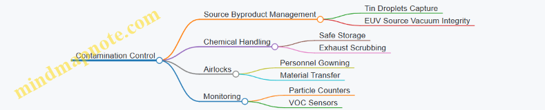
Example 2: Vibration Isolation for EUV Tools
Scenario: EUV scanners are highly sensitive to vibrations that can blur the lithography pattern.
Best Practice: Incorporate floating floor systems and active vibration dampers beneath the EUV tools.
Implementation:
- Design isolated tool bays with concrete slabs mounted on pneumatic isolators.
- Use active feedback systems that detect and counteract vibrations in real-time.
Result: Enhanced pattern fidelity and improved critical dimension uniformity.
Example 3: Power and Cooling Infrastructure
Scenario: EUV tools consume significant power and generate heat that can destabilize the process.
Best Practice: Deploy dedicated power lines with uninterruptible power supplies (UPS) and high-capacity chilled water cooling systems.
Implementation:
- Separate EUV tool power circuits from other fab equipment to prevent interference.
- Use redundant cooling loops to ensure continuous operation during maintenance.
Result: Stable tool operation with minimized downtime.
Summary
Facility design to support EUV process requirements is a multidisciplinary effort combining cleanroom technology, mechanical engineering, electrical infrastructure, and contamination control. By applying best practices such as stringent environmental controls, vibration isolation, and robust power/cooling systems, fabs can maximize EUV tool performance and yield.
For fab process engineers, yield engineers, and equipment engineers, understanding these design principles and their practical implementation is critical to successful EUV integration and advanced CMOS process scaling.
8.5 Regulatory Compliance and Industry Standards
In advanced CMOS process scaling and EUV process controls, adherence to regulatory compliance and industry standards is critical to ensure product quality, environmental safety, and operational reliability. This section explores the key regulations, standards, and best practices semiconductor fabs must follow, along with practical examples and mind maps to clarify complex relationships.
Importance of Regulatory Compliance in Semiconductor Fabrication
- Ensures safety of personnel and environment
- Guarantees product reliability and quality
- Avoids costly legal penalties and production shutdowns
- Facilitates market acceptance and customer trust
Key Regulatory Bodies and Standards
Regulatory Bodies:
- OSHA (Occupational Safety and Health Administration): Worker safety regulations
- EPA (Environmental Protection Agency): Environmental protection and waste management
- REACH (Registration, Evaluation, Authorization and Restriction of Chemicals): Chemical safety in EU
- RoHS (Restriction of Hazardous Substances Directive): Limits hazardous materials in electronics
- ISO (International Organization for Standardization): Quality and environmental management standards
Industry Standards:
- ISO 9001: Quality management systems
- ISO 14001: Environmental management systems
- SEMI Standards: Semiconductor Equipment and Materials International standards for equipment, materials, and processes
- JEDEC Standards: Semiconductor engineering standards
Mind Map: Regulatory Compliance Framework in Semiconductor Fabrication
Best Practices for Compliance Implementation
- Comprehensive Documentation: Maintain detailed records of process parameters, chemical usage, and safety checks.
- Regular Audits: Conduct internal and external audits to ensure adherence to standards.
- Training Programs: Continuous education for fab personnel on regulatory updates and safety practices.
- Chemical Inventory Management: Use automated systems to track hazardous materials and ensure compliance with REACH and RoHS.
- Waste Treatment and Emission Controls: Implement advanced filtration and abatement systems to meet EPA requirements.
Example: Implementing RoHS Compliance in EUV Process
Scenario: A fab introduces a new EUV resist containing trace amounts of restricted substances.
Action Steps:
- Analyze resist chemical composition against RoHS restricted substance list.
- Collaborate with suppliers to certify material compliance.
- Update material declarations and maintain documentation.
- Train process engineers on handling and disposal protocols.
Outcome: Successful RoHS compliance ensured with zero production delays or regulatory fines.
Mind Map: Industry Standards Relevant to EUV Process Controls
Case Study: Achieving ISO 14001 Certification in an EUV Fab
Background: A semiconductor fab aimed to reduce environmental impact while scaling CMOS nodes using EUV lithography.
Implementation:
- Conducted environmental impact assessment focusing on EUV source emissions and chemical waste.
- Installed advanced abatement systems and optimized chemical usage.
- Developed environmental management system aligned with ISO 14001.
- Trained employees on environmental policies and emergency response.
Result:
- Achieved ISO 14001 certification within 12 months.
- Reduced hazardous waste by 25%.
- Improved community relations and regulatory rapport.
Summary
Regulatory compliance and adherence to industry standards are foundational pillars for successful advanced CMOS scaling and EUV process control. By integrating comprehensive safety, environmental, and quality management practices, fabs can maintain high yield, ensure worker safety, and meet global market requirements.
For fab process engineers, yield engineers, and equipment engineers, understanding and applying these regulations and standards is not just a legal obligation but a strategic advantage in the competitive semiconductor landscape.
9. Case Studies and Real-World Applications
9.1 Scaling Challenges and Solutions at Leading Foundries
As semiconductor nodes shrink below 7nm, leading foundries face a complex landscape of scaling challenges that impact yield, performance, and manufacturability. This section explores these challenges and highlights practical solutions implemented by industry leaders such as TSMC, Samsung, and Intel.
Key Scaling Challenges
- Lithography Limitations
- Resolution constraints
- Stochastic defects
- Mask complexity
- Process Variability
- Critical dimension (CD) variation
- Line edge roughness (LER)
- Overlay errors
- Material and Device Integration
- High-k/metal gate stack scaling
- Contact resistance
- FinFET and GAA transistor challenges
- Yield and Defect Management
- Stochastic defectivity in EUV
- Particle contamination
- Equipment-induced variation
Mind Map: Scaling Challenges at Leading Foundries
Solutions and Best Practices
-
Advanced EUV Lithography Implementation
- Increasing source power and dose control to reduce stochastic defects.
- Using multi-beam mask writers and improved mask inspection tools to minimize mask defects.
- Example: TSMC’s adoption of high-power EUV sources and enhanced pellicle technology reduced defectivity by over 30% in 5nm production.
-
Process Control and Metrology Enhancements
- Deploying in-line CD-SEM and scatterometry with AI-driven analytics to monitor and correct CD and overlay variations in real time.
- Example: Samsung’s integration of machine learning algorithms for overlay correction improved overlay accuracy by 15% at 7nm.
-
Material and Device Innovations
- Transitioning to gate-all-around (GAA) transistor architectures to improve electrostatic control and scaling.
- Optimizing high-k/metal gate deposition processes to reduce contact resistance.
- Example: Intel’s RibbonFET GAA technology demonstrated improved drive current and reduced leakage at 4nm.
-
Yield Enhancement through Defect Reduction
- Implementing advanced particle control in cleanrooms and EUV tool chambers.
- Using advanced defect inspection and classification systems to rapidly identify yield detractors.
- Example: Collaborative yield improvement programs at multiple foundries reduced EUV-related stochastic defects by 20%.
Mind Map: Solutions to Scaling Challenges
Real-World Example: TSMC 5nm Node
- Challenge: High stochastic defectivity in EUV patterning causing yield loss.
- Solution: Implemented high-power EUV sources with improved dose stability and introduced advanced pellicles to protect masks.
- Result: Achieved a 30% reduction in defectivity, enabling high-volume manufacturing with competitive yields.
Real-World Example: Samsung 7nm Node
- Challenge: Overlay errors impacting multi-patterning accuracy.
- Solution: Integrated AI-driven overlay correction algorithms with enhanced in-line metrology tools.
- Result: Improved overlay accuracy by 15%, reducing rework and scrap rates.
Summary
Leading foundries address scaling challenges through a combination of advanced lithography techniques, enhanced process control, material innovation, and rigorous yield management. The integration of AI and machine learning into metrology and defect inspection is proving critical in pushing the limits of CMOS scaling while maintaining manufacturability and yield.
For Fab Process Engineers, Yield Engineers, and Equipment Engineers, understanding these challenges and solutions is essential for driving continuous improvement in advanced CMOS manufacturing.
9.2 Yield Improvement through EUV Process Optimization
Yield improvement is a critical objective in semiconductor manufacturing, especially as advanced CMOS nodes leverage EUV lithography. EUV introduces unique challenges such as stochastic defects, mask defects, and resist sensitivity issues that can impact yield. This section explores best practices and optimization strategies to enhance yield through EUV process control, supported by practical examples and mind maps.
Key Factors Affecting Yield in EUV Lithography
Best Practices for Yield Improvement
Stochastic Defect Mitigation
- Practice: Optimize resist formulation and processing parameters to reduce stochastic variations.
- Example: A foundry implemented a new chemically amplified resist with enhanced acid diffusion control, reducing line edge roughness (LER) and stochastic defects by 30%.
Mask Defect Management
- Practice: Employ advanced pellicle materials with high EUV transmittance and robust defect inspection.
- Example: Using a new pellicle design with 90% transmittance improved mask defect coverage, reducing defect-related yield loss by 15%.
Process Window Optimization
- Practice: Tighten focus and dose control through in-line metrology and APC systems.
- Example: Real-time dose adjustment based on scatterometry feedback reduced critical dimension (CD) variation by 10%, improving device performance consistency.
Etch Process Refinement
- Practice: Develop etch recipes that minimize pattern collapse and maintain profile fidelity.
- Example: Switching to a gentler plasma etch chemistry preserved delicate EUV patterns, increasing yield by 8% in a 5nm node process.
Mind Map: EUV Yield Improvement Strategies
Practical Example: Yield Enhancement at a Leading Foundry
A leading semiconductor foundry faced yield degradation due to stochastic defects in their 7nm EUV process. By implementing a multi-pronged approach:
- Switched to a next-generation resist with improved acid diffusion control.
- Enhanced pellicle inspection and cleaning frequency.
- Integrated advanced APC tools for real-time dose and focus adjustments.
- Optimized etch chemistry to reduce pattern collapse.
Result: Yield improved by 20% over six months, with a significant reduction in random defect density and improved device uniformity.
Summary
Yield improvement through EUV process optimization requires a holistic approach addressing resist chemistry, mask quality, process control, and integration steps. Leveraging advanced metrology, APC, and continuous feedback loops enables process engineers to identify and mitigate yield detractors effectively.
By applying these best practices and learning from real-world examples, fab process engineers, yield engineers, and equipment engineers can collaboratively drive yield enhancements critical for the success of advanced CMOS scaling.
9.3 Equipment Engineering Success Stories
In the realm of advanced CMOS process scaling and EUV lithography, equipment engineering plays a pivotal role in ensuring tool performance, uptime, and process consistency. This section highlights several success stories where equipment engineers have driven significant improvements, showcasing best practices and practical examples.
Success Story 1: Predictive Maintenance Reduces EUV Tool Downtime by 30%
Background: A leading semiconductor fab faced frequent unplanned downtime on their EUV scanners, impacting wafer throughput and yield.
Approach: Equipment engineers implemented a predictive maintenance program leveraging sensor data analytics and machine learning algorithms to forecast potential failures before they occurred.
Outcome: Downtime was reduced by 30%, and maintenance costs decreased by 20%. Real-time alerts allowed for scheduled interventions, minimizing impact on production.
Example: Using vibration and temperature sensor data from the EUV source, engineers identified early signs of bearing wear, scheduling replacements proactively.
Success Story 2: Contamination Control Enhances Pattern Fidelity
Background: Contamination on EUV masks and optics was causing stochastic defects, leading to yield loss.
Approach: Equipment engineers redesigned the tool’s internal airflow and introduced advanced filtration systems. Additionally, they optimized cleaning protocols for masks and optics.
Outcome: Defect density related to contamination dropped by 40%, improving overall wafer yield.
Example: Implementation of a laminar airflow system inside the scanner reduced particle deposition on the reticle stage.
Success Story 3: Tool Matching Optimization for Consistent Process Results
Background: Variability between multiple EUV scanners led to inconsistent critical dimension (CD) control across production lots.
Approach: Engineers developed a comprehensive tool matching program involving calibration standardization, cross-tool metrology correlation, and synchronized maintenance schedules.
Outcome: CD variation between tools was reduced from ±3nm to ±1nm, enabling tighter process windows and higher yield.
Example Mind Map:
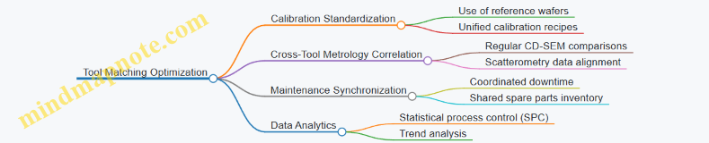
Success Story 4: Automation of EUV Source Alignment Improves Throughput
Background: Manual alignment of the EUV source optics was time-consuming and prone to human error.
Approach: Equipment engineers integrated automated alignment routines using advanced sensors and feedback control loops.
Outcome: Alignment time was cut by 50%, and source stability improved, leading to higher wafer throughput.
Example: The system used interferometric sensors to detect misalignments and automatically adjust mirror positions in real-time.
Success Story 5: Implementation of Remote Monitoring for Proactive Issue Resolution
Background: Equipment failures were often detected only after impacting production.
Approach: A remote monitoring system was deployed, enabling equipment engineers to track tool health metrics 24/7 and respond proactively.
Outcome: Early detection of anomalies reduced emergency repairs by 35% and improved overall equipment effectiveness (OEE).
Example Mind Map:
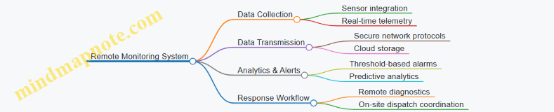
Summary Mind Map: Key Elements of Equipment Engineering Success
These success stories demonstrate how equipment engineers contribute critically to the advancement of CMOS scaling and EUV process control. By combining data-driven approaches, automation, and cross-disciplinary collaboration, they enable fabs to achieve higher yields, better tool uptime, and consistent process results.
9.4 Cross-Disciplinary Collaboration in Process Development
In advanced CMOS process scaling and EUV process controls, cross-disciplinary collaboration is not just beneficial—it is essential. The complexity of modern semiconductor fabrication demands seamless integration of expertise from process engineers, yield engineers, equipment engineers, metrology specialists, and data scientists. This section explores how collaborative efforts accelerate innovation, improve yield, and optimize tool performance, supported by practical examples and mind maps to visualize the synergy.
Why Cross-Disciplinary Collaboration Matters
- Complexity of Advanced Nodes: Sub-10nm nodes involve intricate process steps where lithography, etch, deposition, and inspection must be tightly coordinated.
- EUV Specific Challenges: EUV introduces unique challenges such as stochastic defects, mask contamination, and source stability that require combined expertise.
- Yield and Throughput Optimization: Yield engineers need real-time data from equipment engineers and process engineers to identify and mitigate defects.
- Rapid Problem Solving: Cross-functional teams can quickly identify root causes and implement corrective actions.
Mind Map: Key Stakeholders and Their Roles in Process Development
Example 1: Collaborative Yield Improvement for Stochastic Defects in EUV
Scenario: A foundry experiences yield degradation due to stochastic defects in EUV lithography layers.
Collaboration Approach:
- Process engineers identify process windows and resist sensitivity.
- Yield engineers analyze defect distribution and correlate with process parameters.
- Equipment engineers review scanner performance logs and source stability.
- Metrology specialists enhance inspection sensitivity to detect early defect signatures.
- Data scientists develop predictive models to flag wafers at risk.
Outcome: By integrating insights, the team adjusts resist coating parameters, tunes scanner focus and dose, and implements inline monitoring, resulting in a 15% yield improvement within two production cycles.
Mind Map: Collaborative Workflow for Yield Improvement
Example 2: Equipment Maintenance and Process Stability
Scenario: Frequent EUV scanner downtime causes process variability and delays.
Collaboration Approach:
- Equipment engineers share maintenance schedules and failure modes.
- Process engineers identify process steps sensitive to tool variations.
- Yield engineers monitor wafer-to-wafer variation linked to tool status.
- Data scientists implement predictive maintenance algorithms using equipment sensor data.
Outcome: Predictive maintenance reduces unplanned downtime by 30%, stabilizing process conditions and improving wafer throughput.
Best Practices for Effective Cross-Disciplinary Collaboration
- Regular Cross-Functional Meetings: Establish weekly sync-ups to share data, challenges, and progress.
- Shared Data Platforms: Use centralized databases and dashboards accessible to all stakeholders.
- Joint Root Cause Analysis Sessions: Combine expertise to analyze defects and process excursions.
- Cross-Training: Encourage engineers to gain basic understanding of adjacent disciplines.
- Collaborative Problem-Solving Tools: Utilize mind maps, fishbone diagrams, and workflow charts.
Mind Map: Best Practices for Collaboration
Summary
Cross-disciplinary collaboration in advanced CMOS and EUV process development transforms isolated expertise into a powerful, integrated problem-solving force. By leveraging diverse perspectives and data-driven approaches, semiconductor fabs can accelerate innovation, improve yield, and maintain competitive advantage in the era of extreme scaling.
9.5 Lessons Learned and Future Outlook
As semiconductor fabrication advances deeper into sub-7nm nodes, the integration of EUV lithography and advanced CMOS process scaling has revealed critical lessons and paved the way for future innovations. This section synthesizes key learnings from industry experience and outlines the outlook for process engineers, yield engineers, and equipment engineers.
Key Lessons Learned
-
EUV Process Complexity Requires Holistic Integration
- EUV lithography is not a standalone solution; it demands tight integration with etch, deposition, and metrology processes.
- Example: At a leading foundry, early EUV adoption revealed that without optimized resist materials and etch recipes, CD uniformity suffered despite excellent EUV exposure.
-
Defect Management is Paramount
- Stochastic defects inherent to EUV exposure require advanced inspection and classification methods.
- Example: Machine learning-based defect classifiers reduced false positives by 30%, enabling faster yield ramp.
-
Equipment Stability and Maintenance Directly Impact Yield
- Predictive maintenance and contamination control have become essential to minimize downtime and maintain process window.
- Example: Implementing real-time tool health monitoring reduced unplanned downtime by 25%.
-
Cross-Functional Collaboration Accelerates Problem Solving
- Process, yield, and equipment engineers working in tandem enable faster root cause analysis and corrective actions.
- Example: A joint task force resolved a critical overlay issue within two weeks, preventing a potential yield loss.
-
Advanced Process Control (APC) and Automation are Game-Changers
- Real-time feedback loops and AI-driven control systems enhance process stability and throughput.
- Example: Automated dose and focus control in EUV exposure improved CD uniformity by 15%.
Mind Map: Lessons Learned
Future Outlook
-
Continued EUV Enhancement
- Higher source power and improved mask defect mitigation will push throughput and yield.
- Example: Next-gen EUV sources targeting >500W power to support sub-3nm nodes.
-
Beyond EUV: Next-Generation Lithography
- Techniques like High-NA EUV, Directed Self-Assembly (DSA), and Nanoimprint Lithography (NIL) are under exploration.
- Example: High-NA EUV expected to enable finer patterning with improved depth of focus.
-
AI and Data Analytics Expansion
- Leveraging big data and AI for predictive yield modeling and autonomous process control.
- Example: AI-driven defect prediction models enabling proactive process adjustments.
-
Materials Innovation
- Development of novel resist chemistries and advanced high-k dielectrics to sustain scaling.
- Example: Chemically amplified resists with enhanced EUV sensitivity reducing stochastic defects.
-
Sustainability and Energy Efficiency
- Focus on reducing energy consumption and environmental footprint of EUV tools and fabs.
- Example: Implementation of energy recovery systems in EUV source modules.
Mind Map: Future Outlook
Final Example: Integrating Lessons into Practice
At a recent 5nm node production ramp, a foundry implemented a comprehensive strategy combining enhanced EUV source stability, ML-based defect inspection, and AI-driven APC. This integrated approach led to a 20% yield improvement and a 15% reduction in cycle time, demonstrating the power of applying lessons learned with forward-looking technologies.
In conclusion, the journey of advanced CMOS process scaling with EUV lithography is a continuous learning process. Embracing integrated process controls, leveraging AI, and fostering cross-disciplinary collaboration will be critical to overcoming future scaling challenges and sustaining semiconductor innovation.
10. Conclusion and Future Directions in CMOS Scaling and EUV Control
10.1 Summary of Best Practices and Key Takeaways
As we conclude our deep dive into Advanced CMOS Process Scaling and EUV Process Controls, it is essential to consolidate the best practices and key insights that have emerged throughout the journey. These practices are critical for Fab Process Engineers, Yield Engineers, and Equipment Engineers aiming to optimize performance, yield, and reliability in cutting-edge semiconductor fabrication.
Mind Map: Best Practices Overview
Key Takeaways & Examples
Process Optimization
- Best Practice: Maintain tight control over critical dimensions and uniformity to ensure device performance.
- Example: At a 7nm node fab, implementing advanced etch endpoint detection reduced CD variation by 15%, improving transistor speed consistency.
EUV Lithography
- Best Practice: Stabilize EUV source power and rigorously manage mask defects to reduce stochastic failures.
- Example: A foundry increased EUV source uptime by 20% through enhanced source cleaning protocols, directly boosting wafer throughput.
Metrology & Inspection
- Best Practice: Integrate in-line metrology with machine learning algorithms for rapid defect classification and process feedback.
- Example: Deploying ML-based defect classifiers reduced false positives by 30%, enabling faster yield ramp-up.
Yield Enhancement
- Best Practice: Use comprehensive root cause analysis combined with SPC to identify and mitigate yield detractors.
- Example: Identifying a correlation between resist coating thickness variation and yield loss led to process recipe adjustments, improving yield by 5%.
Equipment Engineering
- Best Practice: Implement predictive maintenance and strict contamination control to minimize tool downtime and variability.
- Example: Predictive analytics on EUV scanner components forecasted failures 2 weeks in advance, preventing unexpected downtime.
Automation & Advanced Process Control (APC)
- Best Practice: Automate dose and focus adjustments in real-time during EUV exposure to maintain process window stability.
- Example: Real-time APC reduced overlay errors by 10%, enhancing multi-layer alignment accuracy.
Environmental & Safety
- Best Practice: Optimize energy consumption and enforce strict safety protocols to ensure sustainable and safe fab operations.
- Example: Retrofitting EUV tools with energy-efficient components cut power usage by 12%, aligning with green fab initiatives.
Mind Map: Example Workflow for Yield Improvement

Final Thoughts
Adopting these best practices with a holistic view—integrating process engineering, metrology, equipment maintenance, and automation—enables semiconductor fabs to successfully scale CMOS technologies while leveraging EUV lithography. Continuous learning, cross-disciplinary collaboration, and embracing emerging AI-driven tools will be pivotal in overcoming future challenges in semiconductor fabrication.
10.2 Emerging Technologies Impacting CMOS Scaling
As CMOS technology approaches its physical and economic limits, emerging technologies are playing a pivotal role in sustaining and advancing semiconductor scaling. These innovations not only complement traditional CMOS scaling but also open new avenues for performance, power efficiency, and integration density.
Key Emerging Technologies
Mind Map: Gate-All-Around (GAA) Transistors
Mind Map: 3D Integration and Heterogeneous Integration
Example: AI-Driven Process Control in CMOS Scaling
In a leading-edge fab, machine learning algorithms analyze in-line metrology data to predict and classify defects during EUV lithography. By correlating process parameters such as dose, focus, and resist thickness with defect patterns, the fab implemented real-time feedback loops that reduced stochastic defect rates by 30%, significantly improving yield and reducing rework.
Example: Advanced Materials for High-Mobility Channels
Intel’s research into germanium (Ge) channels for pMOS devices demonstrates a 20% improvement in hole mobility compared to silicon. This advancement enables higher drive currents and lower power consumption at scaled nodes. Integration challenges such as lattice mismatch and thermal budget are addressed through selective epitaxy and optimized annealing processes.
Summary
Emerging technologies are critical to overcoming the limitations of traditional CMOS scaling. By integrating innovations such as GAA transistors, 3D integration, advanced materials, and AI-driven process controls, the semiconductor industry can continue to deliver performance improvements and cost efficiencies. Understanding these technologies and their practical implementation examples equips process engineers, yield engineers, and equipment engineers to navigate the future of semiconductor fabrication effectively.
10.3 The Role of EUV in Next-Generation Semiconductor Nodes
As semiconductor technology advances beyond the 5nm node, Extreme Ultraviolet (EUV) lithography has become a cornerstone technology enabling continued scaling and innovation. EUV’s ability to pattern smaller features with fewer process steps makes it indispensable for next-generation nodes such as 3nm and beyond.
Mind Map: EUV’s Role in Next-Generation Nodes
Key Advantages of EUV in Advanced Nodes
-
Higher Resolution Patterning: EUV uses a 13.5 nm wavelength, significantly shorter than deep ultraviolet (DUV) lithography, enabling patterning of features below 10 nm with fewer patterning steps.
-
Reduced Multi-Patterning Complexity: Traditional DUV requires multiple patterning steps (double, quadruple patterning) to achieve small features, increasing cost and defect risk. EUV reduces or eliminates these steps, improving yield and throughput.
-
Improved Overlay Accuracy: EUV tools offer better overlay control, critical for multi-layer device fabrication at advanced nodes.
Challenges and Mitigation Examples
-
Stochastic Defects: Random photon shot noise can cause pattern variations.
- Example: Implementing optimized resist formulations and dose control strategies reduces stochastic defects, as demonstrated in a leading foundry’s 5nm node production.
-
Source Power Limitations: EUV source power affects throughput.
- Example: Incremental source power improvements from 250W to 400W have enabled higher wafer per hour (WPH) rates in 3nm node fabs.
-
Mask Defectivity: EUV masks are reflective and more complex.
- Example: Advanced mask inspection and repair techniques have minimized defect-related yield loss in high-volume manufacturing.
Applications of EUV in Next-Gen Nodes
-
Contact and Via Layers: EUV enables precise patterning of contacts and vias with minimal overlay errors.
-
Metal Layers: Complex interconnect patterns benefit from EUV’s resolution and reduced multi-patterning.
-
Gate Patterning: EUV facilitates gate-first and gate-last processes with enhanced critical dimension control.
Process Innovations Supporting EUV Adoption
-
High-NA EUV Development: Next-generation EUV tools with higher numerical aperture (NA) will push resolution further, enabling sub-3nm patterning.
-
Resist Material Advancements: New resist chemistries improve sensitivity and reduce line edge roughness.
-
Enhanced Process Control: Integration of real-time metrology and AI-driven feedback loops optimizes EUV exposure and reduces variability.
Example: 3nm Node Implementation
A leading semiconductor manufacturer successfully integrated EUV lithography for critical layers at the 3nm node, reducing patterning steps by 30% compared to 5nm. This resulted in a 15% improvement in yield and a 10% reduction in cycle time. Key to this success was the deployment of advanced resist materials and in-line metrology for stochastic defect monitoring.
Summary
EUV lithography is pivotal for sustaining Moore’s Law as CMOS technology scales into the sub-5nm regime. While challenges remain, continuous improvements in source power, resist materials, mask technology, and process control are enabling EUV to meet the demands of next-generation semiconductor nodes, driving performance, power efficiency, and cost-effectiveness in future devices.
10.4 Preparing for Beyond EUV: Alternative Lithography Techniques
As semiconductor nodes continue to shrink beyond the limits of Extreme Ultraviolet (EUV) lithography, the industry is actively exploring alternative lithography techniques to sustain Moore’s Law and meet the increasing demand for higher performance and lower power devices. This section delves into these emerging technologies, their principles, challenges, and practical examples, helping fab process engineers, yield engineers, and equipment engineers prepare for the post-EUV era.
Overview of Limitations of EUV Lithography
- Wavelength Constraints: EUV uses 13.5 nm wavelength light, but further scaling demands even shorter wavelengths or different approaches.
- Stochastic Defects: Random photon shot noise causing line edge roughness and pattern fidelity issues.
- Mask Defects and Complexity: Increasing mask complexity and defectivity challenges.
- Throughput and Cost: High tool cost and limited throughput impacting manufacturing economics.
Alternative Lithography Techniques Mind Map
Directed Self-Assembly (DSA)
DSA leverages the natural phase separation of block copolymers to create nanoscale patterns beyond the resolution of conventional lithography.
Example:
- Contact Hole Shrink: Using DSA to reduce contact hole diameters below EUV resolution limits.
- Best Practice: Precise control of polymer composition and annealing conditions to minimize defects.
Mind Map:
Nanoimprint Lithography (NIL)
NIL physically molds patterns into resist layers, enabling sub-10 nm features with potentially lower cost.
Example:
- Bit Patterned Media: High-density magnetic storage media fabrication.
- Best Practice: Mold fabrication with ultra-smooth surfaces and defect-free patterns.
Mind Map:
Electron Beam Lithography (EBL)
EBL offers direct-write patterning with extremely high resolution but limited throughput, making it ideal for mask making and prototyping.
Example:
- Mask Fabrication: Writing complex EUV masks with nanometer precision.
- Best Practice: Proximity effect correction algorithms to ensure pattern fidelity.
Mind Map:
Emerging Concepts and Hybrid Approaches
- Multi-beam EBL: Using arrays of electron beams to increase throughput.
- Nano-Optical Lithography: Exploiting plasmonics to focus light beyond diffraction limits.
- Hybrid DSA + EUV: Combining EUV patterning with DSA for enhanced resolution and defect control.
Example:
- A foundry integrating DSA to complement EUV for contact hole patterning, reducing cost and improving yield.
Preparing Fab Processes for Beyond EUV
- Cross-Disciplinary Collaboration: Integrate materials science, chemistry, and equipment engineering early.
- Pilot Lines and Test Chips: Develop test vehicles to evaluate alternative lithography impact.
- Metrology Development: Invest in new metrology tools compatible with novel patterning techniques.
- Process Integration: Adapt etch, deposition, and cleaning steps to new patterning materials and structures.
Example:
- A yield engineer implementing new SPC charts to monitor DSA defectivity trends alongside EUV metrics.
Summary
Preparing for lithography beyond EUV requires a comprehensive understanding of alternative patterning methods, their integration challenges, and best practices. By leveraging examples such as DSA contact hole shrink and NIL mold fabrication, engineers can proactively adapt their processes and equipment to maintain competitive edge in semiconductor fabrication.
For further reading and detailed case studies, refer to the latest industry whitepapers and technology roadmaps from leading semiconductor consortia.
10.5 Final Thoughts: Continuous Improvement in Semiconductor Fabrication
Continuous improvement is the cornerstone of progress in semiconductor fabrication, especially as we push the boundaries of CMOS scaling and EUV process controls. As process engineers, yield engineers, and equipment engineers, embracing a culture of ongoing refinement ensures that we meet the ever-increasing demands for performance, power efficiency, and cost-effectiveness.
Mind Map: Continuous Improvement in Semiconductor Fabrication
Key Areas for Continuous Improvement with Examples
-
Process Optimization
- Example: Implementing real-time scatterometry feedback during EUV exposure to dynamically adjust focus and dose, reducing critical dimension (CD) variability by 15%.
- Practice: Regularly update process recipes based on in-line metrology data to adapt to tool drift and material variations.
-
Yield Enhancement
- Example: Using machine learning algorithms to classify and predict defect patterns from wafer inspection data, enabling targeted process corrections that improved yield by 8%.
- Practice: Conduct thorough root cause analysis sessions involving cross-disciplinary teams to identify and eliminate yield detractors.
-
Equipment Reliability
- Example: Deploying predictive maintenance schedules for EUV scanners based on vibration and temperature sensor data, reducing unplanned downtime by 20%.
- Practice: Establish stringent contamination control protocols and regular tool calibration to maintain consistent process performance.
-
Innovation & Technology Adoption
- Example: Early adoption of AI-driven APC systems that optimize dose and focus parameters in real-time, leading to improved pattern fidelity and throughput.
- Practice: Continuously evaluate emerging lithography and process technologies, preparing pilot runs to assess feasibility and integration.
-
Knowledge Sharing
- Example: Creating a centralized knowledge base with detailed process change logs, troubleshooting guides, and best practice documents accessible to all fab engineers.
- Practice: Organize regular cross-functional workshops and training sessions to disseminate learnings and foster collaboration.
Mind Map: Example Workflow for Continuous Improvement Cycle
Final Example: Continuous Improvement in Action
A leading fab noticed an increase in stochastic defects during EUV lithography at the 5nm node. By integrating advanced in-line metrology with AI-driven defect classification, the team rapidly identified a correlation between resist sensitivity fluctuations and defect rates. They optimized resist bake parameters and updated the exposure dose control algorithms. Subsequent pilot runs showed a 12% reduction in defect density and a corresponding yield increase. This success was documented and shared across process teams, becoming a standard practice for future nodes.
Summary
Continuous improvement in semiconductor fabrication is a dynamic, multi-faceted endeavor. By combining data-driven process optimization, proactive equipment management, innovative technology adoption, and robust knowledge sharing, fabs can sustain competitive advantages and meet the challenges of next-generation CMOS scaling and EUV lithography. Cultivating this mindset and embedding it into daily operations is essential for long-term success.