RISC-V FPGA Prototyping and Open Hardware Design
1. Scope and Workflow for Open RISC-V FPGA Prototyping
1.1 Defining The Target Platform Requirements For FPGA Validation
A good FPGA validation plan starts with a concrete target platform description. “Validate the design” is not a requirement; it’s a wish. Requirements should state what must work, how you will measure it, and what “done” means when you run tests on real hardware.
Start with a One Page Platform Statement
Write a short statement that includes:
- Board and FPGA: exact device model, package, and clock sources you will use.
- Interfaces: UART, SPI, GPIO, Ethernet, JTAG/UART bridges, and any external memory.
- Performance envelope: target clock frequency and acceptable latency for key operations.
- Software expectations: bare-metal only or also a minimal OS, plus the boot method.
- Observability: what signals you can read or capture (UART logs, register probes, debug bus, LEDs).
Example: “Validate a LiteX-based RISC-V SoC on an FPGA board with a 50 MHz clock, UART console at 115200 baud, and a memory-mapped GPIO block. Use UART logs and a register probe bus to confirm boot, CSR reads, and interrupt delivery.”
Define Validation Objectives That Map to Requirements
Validation objectives should be testable and traceable to platform statement items.
Use three layers:
- Bring-up objectives: the system boots and reaches a known software milestone.
- Interface objectives: each external interface behaves correctly under defined traffic.
- Correctness objectives: architectural behaviors you care about, such as exception handling and interrupt timing.
A practical rule: every objective must have at least one measurable artifact—UART line, register value, waveform marker, or pass/fail counter.
Specify Measurable Pass Fail Criteria
For each objective, define:
- Acceptance conditions: exact values or invariants.
- Tolerance: timing windows, baud rate error bounds, and reset settling time.
- Failure signals: what you will treat as a bug.
Example criteria for UART console:
- Boot prints “READY” within 2 seconds of reset deassertion.
- No framing errors reported by the UART receiver logic.
- Characters match expected strings byte-for-byte.
Example criteria for GPIO:
- Writing
0xA5to GPIO output register results in observed pin state within a specified number of cycles. - Reading GPIO input register returns the last driven value.
Identify Constraints That Affect Hardware Behavior
Constraints are not “nice to have”; they shape what you can validate.
Include:
- Clocking: available PLL/MMCM options, clock domain crossings, and reset strategy.
- Memory: whether you use block RAM, external DDR, or both; include address width and alignment rules.
- I/O timing: IO standards, drive strength, and any required synchronizers.
- Resource limits: maximum acceptable logic utilization and BRAM usage for your chosen FPGA.
A common pitfall is ignoring reset behavior. If your SoC uses multiple clock domains, define how long each domain must remain in reset and how you will detect correct release.
Create a Testable Interface Contract
Turn interface expectations into a contract that both hardware and software can follow.
For memory-mapped peripherals, specify:
- Base address and register offsets.
- Register widths and byte lanes.
- Read/write semantics: read-only, write-one-to-clear, read-modify-write requirements.
- Side effects: what happens when you write a control register.
Example contract snippet for a timer:
CTRLat0x00: bit0 enables timer, bit1 clears counter.COUNTat0x04: read-only 32-bit counter.IRQ_STATUSat0x08: write 1 clears pending interrupt.
Your validation tests should exercise the contract directly, not indirectly through assumptions.
Mind Map: Platform Requirements to Validation Artifacts
Example: Turning Requirements into a Concrete Checklist
Use a checklist that you can run before writing tests.
- I can identify the exact FPGA clock frequency and reset deassertion timing.
- I know the UART baud rate and have a known-good “READY” string.
- I have an address map for every peripheral used in tests.
- I defined register semantics for every control/status register.
- I can observe interrupt delivery using a status register or probe.
- I defined timing tolerances for each acceptance condition.
When these items are complete, the rest of the book’s workflow—simulation, software bring-up, and FPGA validation—has a stable target to aim at. Without them, you end up debugging the plan instead of the design.
1.2 Mapping System Requirements to SoC Components and Interfaces
System requirements are easiest to implement when they are translated into three concrete things: (1) what must happen, (2) where it happens, and (3) how blocks talk to each other. In a RISC-V SoC built from Chisel modules and a LiteX SoC wrapper, that translation becomes a mapping exercise from requirements to components and then to interfaces.
Step 1: Classify Requirements by Behavior and Timing
Start by sorting each requirement into one of four buckets.
- Functional behavior: “UART must transmit bytes at a configured baud rate.”
- Performance behavior: “Sustained throughput must not drop below X bytes per second.”
- Timing and sequencing: “Reset must release peripherals after the clock is stable.”
- Observability and control: “Software must read status registers and clear error flags.”
This classification matters because it determines whether you model the block as a pure combinational datapath, a clocked state machine, or a bus-mapped register block with side effects.
Step 2: Choose the SoC Boundary and Bus Style
LiteX typically provides a CPU-to-peripheral bus (often Wishbone) and a memory map. Your mapping should decide what is memory-mapped versus streaming.
- Memory-mapped registers handle configuration, status, and control.
- Memory-mapped buffers handle bulk data transfers when you want simplicity.
- Streaming interfaces handle high-rate data paths when you can afford more wiring and verification.
A good rule: if software needs to poll or configure something, make it a register block; if hardware needs to move data continuously, use a streaming or DMA-like path.
Step 3: Map Each Requirement to a Component Set
For each requirement, identify the smallest set of components that can satisfy it.
Example: “Software must print debug messages over UART.”
- UART TX peripheral: converts bytes into serial line timing.
- UART RX peripheral if you also need command input.
- Clocking and reset logic: ensures baud generator runs from the correct clock.
- Interrupt or status registers: exposes “TX ready” or “RX available.”
- SoC integration glue: connects the peripheral to the bus and assigns addresses.
You can keep the mapping systematic by writing a short “requirement-to-component” row for each item: requirement, component(s), interface type, and verification target.
Step 4: Define Interfaces as Contracts, Not Wiring
Once components are chosen, define interfaces as contracts with explicit signals, semantics, and error behavior.
For bus-mapped peripherals, the contract usually includes:
- Addressing: which address range maps to which registers.
- Read semantics: whether reads are side-effect free or clear-on-read.
- Write semantics: which bits are writable, which are read-only, and which trigger actions.
- Timing: whether reads complete in one cycle or may stall.
For streaming datapaths, the contract includes:
- Valid/ready handshake rules.
- Backpressure behavior when the consumer cannot accept data.
- Packet framing if the stream carries structured messages.
A practical mapping habit: write the interface contract as a mini checklist and then mirror it in both the Chisel module and the LiteX integration.
Mind Map: Requirement to Component to Interface
Example: Mapping a Minimal UART Requirement
Requirement: “Software writes a byte and expects it to appear on the TX pin, with a status bit indicating readiness.”
- Component choice: UART TX plus a small transmit FIFO.
- Register map:
TX_DATAwrite-only register: writing a byte enqueues it.TX_STATUSread-only register: bittx_readyindicates FIFO space.
- Interface contract:
- Writes to
TX_DATAare accepted only when FIFO is not full. - If the FIFO is full, define behavior: either stall bus transactions or drop with an error flag.
- Writes to
- Verification target:
- In simulation, drive bus writes and check that
tx_readytransitions correctly and that the serial output matches expected bit timing.
- In simulation, drive bus writes and check that
This mapping avoids the common failure mode where the peripheral is correct in isolation but the bus semantics are ambiguous, leading to software that “works” only by accident.
Step 5: Ensure the Mapping Produces Testable Interface Points
A mapping is complete when every requirement has at least one testable observation point.
- For functional behavior, observe outputs (UART line, GPIO pins) and status registers.
- For performance behavior, observe FIFO occupancy and interrupt timing.
- For timing and sequencing, observe reset release behavior and first valid transactions.
- For observability, observe error flags and clear behavior.
When you can point to a specific register bit or signal transition for each requirement, the rest of the flow—Chisel implementation, LiteX integration, Verilator tests, and FPGA validation—becomes a straightforward execution of the same contract.
1.3 Selecting Toolchains for Chisel LiteX Verilator and FPGA Flows
A good toolchain choice starts with a simple question: what do you need to prove at each stage? Simulation proves behavior quickly, synthesis proves realizability, and FPGA validation proves timing and integration under real IO and reset behavior. The trick is to pick tools that agree on interfaces and produce artifacts you can trace end to end.
Start with Artifact Boundaries
Chisel produces parameterized RTL, LiteX assembles a SoC around that RTL, Verilator simulates the resulting Verilog, and the FPGA toolchain turns the final design into a bitstream. Treat each boundary as a contract:
- Chisel to Verilog: stable module names, deterministic parameterization, and consistent reset/clock conventions.
- LiteX to Verilog: predictable bus wiring and address maps, plus generated headers or constants that your software can use.
- Verilog to Verilator: cycle-accurate expectations for bus handshakes and interrupt behavior.
- Verilog to FPGA: constraints for clocks, IO standards, and reset synchronization.
If you can describe what files are produced and consumed at each boundary, you can select tools without guessing.
Choose a Chisel Path That Produces Verilog You Can Trust
Prefer a Chisel setup that makes Verilog generation repeatable. Use a single build script that pins the Chisel generator configuration and emits a build manifest. A practical habit: keep the generated Verilog in a build directory keyed by a hash of parameters, so you can reproduce a simulation run months later.
Example: generate Verilog for a small SoC top and verify that the module hierarchy matches what LiteX expects.
# Example Build Flow Sketch
# 1) Generate SoC RTL via LiteX
# 2) Generate Chisel modules used by LiteX
# 3) Collect Verilog into a single simulation and synthesis input set

make soc-verilog
make verilator-sim
make fpga-bitstream
Align LiteX Integration with Simulation Expectations
LiteX can generate SoC glue, but your simulation must model the same bus semantics you will synthesize. Focus on:
- Bus protocol: whether reads are combinational or registered, and how wait states are represented.
- Interrupt wiring: whether interrupts are level or edge sensitive in your peripheral logic.
- Memory map constants: ensure software-visible addresses match the hardware decode.
A simple check is to simulate a peripheral register write and confirm that the decode logic triggers exactly once per transaction.
Use Verilator for Fast Feedback, Not for “Everything”
Verilator is excellent for cycle-level debugging and assertions, but you must configure it to match your design style. Keep these points concrete:
- Clock and reset: drive them explicitly in the testbench; do not rely on implicit initialization.
- Bus transactions: model ready/valid or wishbone-like handshakes with the same timing you expect in hardware.
- Assertions: add checks for illegal states such as reads to unmapped addresses or stalled handshakes.
Example: a minimal testbench loop that performs a write then reads back.
// Pseudocode style example for a bus transaction loop
// Keep it aligned with your LiteX bus semantics.

repeat (1000) begin
  drive_bus_write(addr, data);
  wait_bus_ack();

  drive_bus_read(addr);
  wait_bus_ack();
  if (bus_rdata !== expected) $fatal;

  tick();
end
Select FPGA Tools by Constraint Discipline
FPGA flows differ by vendor, but the selection criteria are the same: can you express constraints clearly, and can you produce timing reports you can interpret? Your goal is to catch issues early:
- Clock constraints: define primary clocks and any derived clocks.
- Reset strategy: ensure reset is synchronized where needed.
- IO constraints: set standards and pin assignments for UART or debug signals.
A practical workflow is to run synthesis with conservative effort first, then tighten constraints only after you confirm the design is structurally correct.
Build a Single Source of Truth for Parameters and Addresses
Toolchains fail when parameters drift. Use one configuration file or one generator script that feeds:
- Chisel parameters
- LiteX SoC configuration
- Software header values for base addresses and register offsets
- Verilator testbench constants
- FPGA top-level generics and constraints
This is boring work, which is exactly why it prevents the most common integration failures.
Mind Map of Toolchain Selection
Mind Map: Selecting Toolchains for Chisel, LiteX, Verilator, and FPGA
A Concrete Selection Checklist
Use this checklist before committing to a flow:
- Can you regenerate the same Verilog from the same parameters and get identical module interfaces?
- Do your LiteX-generated address constants match what your software uses?
- Does your Verilator testbench drive reset and clock explicitly?
- Do you have a clear mapping from bus transactions in simulation to bus transactions in hardware?
- Are your FPGA constraints defined in a way that you can explain in one paragraph?
If any answer is “not yet,” fix that boundary first. Toolchains are easier to choose than to debug, and boundaries are where debugging starts.
1.4 Establishing a Reproducible Build and Test Workflow
Reproducibility is not a vibe; it is a checklist. In an FPGA prototyping flow that spans Chisel, LiteX, Verilator, and vendor tools, the workflow must record inputs, pin versions, and make test results attributable to a specific build. The goal is simple: if you rerun the same command on the same commit, you should get the same artifacts and the same pass or fail.
Foundations That Make Builds Repeatable
Start by treating the repository as the source of truth.
- Pin the toolchain inputs: record the exact versions of Scala, sbt, Chisel, LiteX, Verilator, and the FPGA toolchain. If you use container images, record the image digest, not just the tag.
- Pin the hardware configuration: store SoC parameters (CPU type, memory map, peripheral set, clock/reset settings) in version-controlled files. Avoid “mystery defaults” that change when a library updates.
- Pin the build environment: capture OS-level dependencies (packages, drivers, Python modules) either via a container or a lockfile-driven setup.
- Make artifacts deterministic: ensure generated outputs include the commit hash and configuration hash in their filenames and in a manifest file.
A practical rule: every build directory should contain a manifest that answers “what produced this?” without reading the build scripts.
A Systematic Workflow from Commit to Bitstream
Use a staged pipeline so failures are localized.
Stage A: Generate RTL
- Inputs: Chisel sources, configuration, and tool versions.
- Outputs: Verilog plus a manifest.
- Best practice: run a “clean then build” once per configuration to confirm no hidden state.
Stage B: Simulate the RTL
- Inputs: generated Verilog, testbench, and simulation parameters.
- Outputs: simulation logs, coverage, and pass/fail.
- Best practice: keep the testbench deterministic by fixing random seeds and avoiding time-based waits.
Stage C: Build the SoC and Firmware
- Inputs: LiteX SoC config, memory map, and software sources.
- Outputs: SoC artifacts, firmware binary, and a combined memory map report.
- Best practice: validate that the firmware’s linker script matches the SoC memory map before running simulation.
Stage D: Synthesize and Implement
- Inputs: top-level design, constraints, and FPGA part selection.
- Outputs: bitstream, timing reports, and a build manifest.
- Best practice: archive the synthesis and implementation logs, because they explain timing differences even when the RTL is unchanged.
Mind Map: Reproducible Build and Test Workflow
Example: Makefile-Style Targets with Manifests
This pattern keeps the workflow readable and forces each stage to declare its inputs.
# Example: Staged Workflow with Manifests
BUILD_DIR ?= build
CONFIG ?= configs/base.json
COMMIT ?= $(shell git rev-parse HEAD)

rtl:
	./scripts/gen_rtl.sh --config $(CONFIG) --out $(BUILD_DIR)/rtl --commit $(COMMIT)

sim:
	./scripts/run_verilator.sh --rtl $(BUILD_DIR)/rtl --out $(BUILD_DIR)/sim --seed 1

soc:
	./scripts/build_soc.sh --config $(CONFIG) --rtl $(BUILD_DIR)/rtl --out $(BUILD_DIR)/soc

fpga:
	./scripts/fpga_build.sh --soc $(BUILD_DIR)/soc --out $(BUILD_DIR)/fpga
A good manifest file should include: commit hash, config hash, tool versions, and the exact command lines used for each stage.
Example: Deterministic Simulation Checks
When simulation fails, you want a stable reproduction.
- Fix the seed: always pass a seed value to the testbench.
- Record the simulation command line: store it in the simulation output directory.
- Save the failing trace: keep the waveform or transaction log for the first failing test.
# Example: Deterministic Simulation Invocation
./scripts/run_verilator.sh \
  --rtl build/rtl \
  --out build/sim \
  --seed 1 \
  --tests bus_smoke uart_smoke boot_smoke \
  --save-trace-on-fail
Example: Configuration Hashing for Artifact Naming
Use a hash of the configuration file contents so two different configs never collide.
- Compute
config_hash = sha256(config.json). - Use
build/<config_hash>/<commit>/...for outputs. - Write
manifest.jsoninto each stage directory.
This makes it obvious which artifacts correspond to which settings, even months later.
Advanced Details That Prevent “It Works on My Machine”
- Normalize paths: if your generator embeds absolute paths into outputs, strip or normalize them.
- Control parallelism: parallel builds can reorder generated files; ensure the manifest captures the final file set.
- Validate interface contracts: before simulation, check that the generated memory map matches the software linker expectations.
- Treat constraints as inputs: pin the FPGA part number, package, speed grade, and constraint files in the manifest.
With these practices in place, the workflow becomes a chain of evidence rather than a chain of guesses. When something breaks, you can point to the stage, the inputs, and the exact commands that produced the result.
1.5 Documenting Interfaces Memory Maps and Build Artifacts
Good documentation is what lets a second person (or your future self) reproduce a working system without guessing. For FPGA prototyping, the most valuable artifacts are the ones that connect three worlds: the hardware interface contract, the software-visible memory map, and the exact build outputs that produced a bitstream.
Interface Contracts That Survive Integration
Start by writing down the interface contract before you write the first test. For each bus or peripheral interface, capture: signal names, widths, reset behavior, transaction rules, and error handling. Keep the contract close to the RTL module so it stays accurate.
A practical approach is to define a small “interface header” section in your documentation:
- Clock and reset: which clock domain drives the interface, and whether reset is synchronous or asynchronous.
- Handshake semantics: for ready/valid style buses, specify when
validmay be asserted and whenreadymay be deasserted. - Addressing rules: alignment requirements, byte vs word addressing, and endianness assumptions.
- Read and write timing: whether reads are combinational or registered, and whether writes take effect immediately or on a clock edge.
Example: for a memory-mapped register block, state that reads return the current register value on the cycle after address acceptance, and writes update the register on the rising edge when we is asserted.
Memory Maps That Match Reality
A memory map is not a list of addresses; it is a contract between CPU, interconnect, and peripherals. Document it so software can be written without peeking into RTL.
Include these elements for every region:
- Base address and size: in hex, with the size aligned to the bus granularity.
- Access type: read-only, write-only, read-write, and whether writes are byte-enabled.
- Register layout: offsets, field bit ranges, reset values, and write masks.
- Side effects: whether reads clear status bits, whether writes trigger actions, and whether certain writes are ignored when a busy flag is set.
A small but important best practice is to document “holes” explicitly. If a region is reserved, mark it as such so software doesn’t accidentally rely on undefined behavior.
Example register documentation snippet (human-readable):
0x4000_0000 + 0x00CTRL(RW, reset0x0000_0001)- bit 0
EN: enables the peripheral - bit 1
LOOP: when set, repeats a test pattern
- bit 0
0x4000_0000 + 0x04STATUS(RO, reset0x0000_0000)- bit 0
DONE: set when operation completes - bit 1
ERR: set on bus or internal error
- bit 0
Then add the behavior rule: “Writing CTRL.EN=0 stops the peripheral after the current operation finishes.” That single sentence prevents a lot of confusion.
Keeping Software and Hardware in Lockstep
To avoid mismatches, treat the memory map as a source of truth. Generate software-visible definitions from the same data used to configure the SoC.
Even if you do not fully automate generation, you can still enforce consistency by using a single table format for both hardware and software:
- one table for region ranges
- one table for registers and fields
- one table for interrupt mapping
Example: define an interrupt table that states which peripheral asserts which interrupt line, and whether it is level or edge sensitive. Software then knows whether it must poll or can rely on an interrupt handler.
Build Artifacts That Make Results Reproducible
A build artifact is only useful if it can be traced back to inputs. For each build, record:
- Tool versions: synthesis, place-and-route, and simulation tools.
- Build configuration: SoC parameters, target FPGA part, clock frequency, and constraints file name.
- Generated outputs: Verilog netlists, SoC integration outputs, simulation command logs, and the final bitstream.
- Checksums or hashes: for the bitstream and key intermediate files.
Use a consistent naming scheme so artifacts sort naturally by build. A common pattern is project_target_config_YYYYMMDD_HHMM.
Example build record fields:
bitstream:top_soc_fpgaA_default_20250301_1430.bitnetlist:build/top_soc.vconstraints:constraints/fpgaA.xdcsim_log:logs/verilator_run_20250301_1430.txthashes: SHA256 for bitstream and netlist
Mind Map: What to Document
Example: A Minimal Documentation Template
Interface Contract: UART MMIO
- Clock domain: clk_sys
- Reset: synchronous, active-high
- Addressing: byte addresses, 32-bit aligned
- Read timing: 1-cycle latency after address accept
- Write timing: update on rising edge when we is asserted
- Side effects: writing TX triggers transmit if FIFO not full

Memory Map Summary
- UART region: 0x4000_0000..0x4000_0FFF (4 KiB), RW
- STATUS at +0x04: RO, DONE clears on read

Build Record
- FPGA part: fpgaA
- Constraints: constraints/fpgaA.xdc
- Bitstream: top_soc_fpgaA_default_20250301_1430.bit
- Netlist: build/top_soc.v
- Hashes: sha256(bitstream), sha256(netlist)
This template is intentionally small, but it forces the key decisions into the open: timing, side effects, and traceability. When those are documented clearly, integration work becomes mostly mechanical rather than interpretive.
2. RISC-V Architecture Fundamentals for Hardware Designers
2.1 Privilege Levels and Exception Handling Basics
Privilege levels in RISC-V define what the CPU is allowed to do. Exception handling defines what the CPU does when something goes wrong or needs attention. Together, they form the “rules of the road” for running software safely on hardware.
Privilege Levels as a Permission Model
RISC-V commonly uses at least three privilege modes: Machine (M), Supervisor (S), and User (U). Not every system implements all modes, but the model is consistent.
- Machine mode (M) is the most privileged. Firmware and platform bring-up typically start here.
- Supervisor mode (S) is used by an OS kernel.
- User mode (U) runs applications with restricted access.
A key idea is that instructions that touch sensitive state are either illegal or trapped when executed from insufficient privilege. For example, reading or writing certain control and status registers (CSRs) is allowed only in specific modes. This is why “it works in simulation” can still fail on hardware: the hardware enforces privilege checks.
Exceptions as Synchronous Events
An exception is a synchronous event: it occurs as a direct result of executing an instruction. The CPU records enough information to resume or handle the event.
Common exception categories include:
- Instruction address faults when fetching an instruction from an invalid address.
- Illegal instruction when the instruction encoding is not supported.
- Environment calls used by software to request a service.
- Load/store access faults when memory permissions or addresses are invalid.
When an exception happens, the CPU typically:
- Saves the current execution context into CSRs.
- Jumps to an exception handler address.
- Updates privilege state so the handler runs with appropriate permissions.
The Core CSRs You Will Actually Use
Even if your design later adds more features, these CSRs are the ones you’ll see during bring-up.
mstatusholds global status bits, including the current privilege-related state and interrupt enable fields.mtvecdefines the base address of the machine-mode trap handler.mcauserecords the reason for the trap, usually as a code.mepcstores the program counter value to return to.mtvalmay store additional faulting information, such as a bad address.
Supervisor-mode equivalents exist for S-mode, but the pattern is the same.
How Return Works Without Guesswork
A trap handler often ends with a return instruction that restores control flow. For machine mode, the common return is mret. The CPU uses mepc to resume execution and uses mstatus to restore the previous interrupt enable state.
A subtle but important detail: for many synchronous exceptions, the faulting instruction is the one that caused the trap. That means your handler must decide whether to:
- Re-execute the instruction after fixing state, or
- Advance past it.
Handlers typically adjust mepc when they want to skip the offending instruction. If you don’t, you can end up in a trap loop that looks like a dead system.
Mind Map: Privilege and Exceptions
Example: Environment Call from User Mode
Suppose an application wants a service such as printing a character. A common pattern is to use an environment call instruction. The CPU traps into the handler because the instruction is defined to cause a synchronous exception.
A minimal handler flow is:
- Read
mcauseto confirm the reason. - Read arguments from agreed-upon registers.
- Perform the service.
- Advance or keep
mepcdepending on the calling convention. - Write any return value.
- Execute
mret.
If you forget to advance mepc when the calling convention expects it, the same environment call repeats and the system appears stuck.
Example: Illegal Instruction During Bring-Up
During FPGA bring-up, illegal instruction traps are common when software and hardware disagree about supported extensions. The handler should:
- Inspect
mcauseto identify the illegal instruction exception. - Optionally inspect
mtvalto see the faulting instruction or related info. - Decide whether to halt, report via UART, or fall back to a safe path.
This is also where privilege checks matter: if your handler runs in a mode that lacks permission to read the needed CSRs, you’ll get a second failure. That’s why machine-mode handlers are often used early.
Example: Faulting Load with a Bad Address
A load from an unmapped or forbidden address triggers a load access fault. The handler can use mtval to learn which address caused the problem. Then it can either:
- Terminate the offending task in a controlled way, or
- Map the page and retry, if your system supports that style of recovery.
Even in a simple bare-metal system, you can use this to print a useful error message instead of silently hanging.
Practical Takeaway for Hardware-Software Integration
When you implement or validate a RISC-V core, privilege and exception behavior should be treated as part of the interface, not an afterthought. Your testbench should verify that:
- The correct CSRs are written on each exception.
- The handler entry address is honored.
mretrestores execution correctly.- Faulting instructions don’t cause infinite trap loops due to incorrect
mepchandling.
2.2 Instruction Fetch Decode Execute Pipeline Expectations
A RISC-V core’s pipeline is easiest to reason about when you treat it as a contract between stages: each stage receives inputs with specific timing and validity rules, and each stage produces outputs that downstream logic can trust. In practice, “expectations” means you should know what must be true for correct execution, what can be temporarily false during stalls, and how control flow changes those rules.
Foundational Stage Responsibilities
Instruction Fetch is responsible for producing the next instruction word and the associated program counter (PC). The fetch stage must also respect control-flow changes such as taken branches and jumps. If the PC changes, the fetch stage must not keep feeding instructions from the old path.
Decode translates the raw instruction bits into control signals and operand selections. Decode also typically computes immediate values and determines whether the instruction needs special handling, such as system instructions or memory access alignment checks.
Execute performs the core computation: ALU operations, effective address calculation, branch condition evaluation, and sometimes early CSR or privilege checks. Execute is also where many pipelines decide whether to redirect the PC.
A useful mental model is that each stage has a “valid” signal. When valid is false, downstream logic should ignore the stage’s outputs. When valid is true, downstream logic can assume the outputs correspond to the stage’s inputs.
Timing Expectations Across Cycles
In a simple in-order pipeline, you can expect one instruction to enter fetch each cycle under steady conditions. However, correctness depends on how the pipeline handles hazards.
- Data hazards occur when an instruction needs a value that a previous instruction has not produced yet.
- Control hazards occur when the next PC depends on a branch or jump decision.
- Structural hazards occur when two stages need the same resource at the same time.
Most FPGA prototypes aim for a predictable baseline: in-order issue, explicit stalling, and clear forwarding paths. If you implement forwarding, the execute stage may receive operands from later pipeline stages rather than waiting for register file writeback.
Control Flow Expectations
Branches and jumps change the PC. The pipeline must ensure that instructions fetched along the wrong path do not commit architectural state.
Common expectations you should verify:
- PC redirect latency: how many cycles after decode or execute the new PC takes effect.
- Flush behavior: which pipeline stages are invalidated when a redirect occurs.
- Branch decision source: whether the branch condition is evaluated in execute (typical) or earlier.
If your design evaluates branch conditions in execute, then instructions in fetch and decode for the wrong path may already be in flight. The pipeline must mark them invalid and prevent their results from reaching writeback.
Data Hazard Expectations
For RISC-V, the most common hazard is a consumer instruction using a register written by a producer instruction. Your pipeline should define:
- Forwarding coverage: which producer stages can forward to execute.
- Load-use handling: loads often produce data later than ALU results, so the consumer may need a stall.
- Register file timing: whether writeback happens early enough in the cycle for same-cycle reads.
A concrete example helps. Suppose instruction A produces x5 and instruction B uses x5:
- If A is an ALU op, forwarding from execute or memory stage may satisfy B without stalling.
- If A is a load, the data may only be available after memory access, so B may need one stall cycle.
Decode Expectations for Correctness
Decode must generate correct control signals for every instruction class. That includes:
- Immediate decoding for each instruction format.
- Register index extraction and correct handling of x0 as hardwired zero.
- CSR access rules: privilege checks and illegal instruction detection.
- Memory access semantics: load/store width and sign extension behavior.
Even when the execute stage is where the action happens, decode is where many “off by one bit slice” bugs originate. Treat decode as a deterministic translator from instruction bits to control.
Mind Map: Pipeline Expectations
Example: Branch Redirect and Flush
Consider:
- Cycle N: fetch instruction at PC=100
- Cycle N+1: decode instruction at PC=100; fetch instruction at PC=104
- Cycle N+2: execute determines branch is taken to PC=200
Expectations:
- The instruction fetched at PC=104 (and any younger instructions) must be marked invalid before they can update architectural state.
- The next valid fetch after the redirect should target PC=200, with its own valid flag asserted.
If you observe that PC=200 is fetched but the instruction at PC=104 still writes a register, your flush/valid gating is incomplete.
Example: Load-Use Hazard
Consider:
- Instruction A:
lw x5, 0(x1) - Instruction B:
add x6, x5, x7
If the pipeline can forward ALU results but not load data until after memory access, then B must not execute with an old x5 value. The expectation is either:
- Stall B in decode until x5 is available for execute, or
- Provide a dedicated path that forwards load data to execute at the correct cycle.
A simple check is to run a program where x5 is initialized to a known value, then immediately overwritten by the load, and confirm that x6 reflects the loaded value rather than the stale one.
Practical Validation Checklist
When you prototype, treat these as pass/fail expectations:
- Valid gating: no writeback occurs from invalidated instructions.
- Forwarding correctness: consumer results match a reference model for back-to-back ALU dependencies.
- Load-use timing: consumer results match for immediate load followed by dependent ALU.
- Branch correctness: taken and not-taken paths both produce correct architectural state.
- CSR and illegal instruction behavior: decode and execute agree on legality and trap behavior.
If these checks hold, the pipeline’s fetch-decode-execute contract is consistent enough that higher-level SoC integration won’t be fighting ghosts.
2.3 Memory Ordering Concepts for Bare Metal and Simple OSes
Memory ordering is the set of rules that decide when one core or device can observe another core’s or device’s writes. On FPGA-based RISC-V prototypes, you’ll feel these rules most when you add interrupts, DMA-like transfers, or shared ring buffers. The goal is simple: make the producer’s data visible before the consumer is told to look.
What “Ordering” Means in Practice
Consider two actions in program order:
- Write data to a shared memory region.
- Set a flag (or publish a pointer) that tells another agent the data is ready.
Without ordering guarantees, the other agent might observe the flag update first, then read stale data. This can happen even if your code writes in the right sequence, because:
- The compiler may reorder independent operations.
- The CPU may buffer writes or allow later operations to complete earlier.
- Interconnects may not preserve visibility timing across masters.
On RISC-V, the memory model is expressed through fences and atomic operations. For bare metal and simple OSes, you typically use a small set of patterns rather than trying to reason about every microarchitectural detail.
The Core Tools: Fences and Atomics
A fence constrains the order in which memory operations become visible to other observers. Think of it as “don’t let these memory effects pass each other.”
- Acquire: prevents later reads/writes from moving before the acquire point. Use when you start consuming shared data after observing a flag.
- Release: prevents earlier reads/writes from moving after the release point. Use when you publish shared data before setting the flag.
- Full fence: blocks both directions. Use when you need stronger guarantees or when you’re unsure which side needs acquire vs release.
Atomic read-modify-write operations (like swap or compare-and-swap) also provide ordering properties, but you still need to choose the correct semantics for your algorithm.
A Systematic Pattern for Producer Consumer
Producer steps
- Write payload fields into shared memory.
- Execute a release fence.
- Store the “ready” flag or update the queue head.
Consumer steps
- Spin until the ready flag is observed.
- Execute an acquire fence.
- Read payload fields.
This pattern ensures that if the consumer sees the ready flag, it also sees the payload writes that happened-before the release.
Example: Flag Publishing for UART-Driven Work
Assume an interrupt handler writes a status block and then sets work_ready. The main loop waits for work_ready and then reads the block.
// Shared memory
struct Status { uint32_t code; uint32_t detail; } status;
volatile uint32_t work_ready;

void publish_status(uint32_t code, uint32_t detail) {
  status.code = code;
  status.detail = detail;
  __asm__ volatile("fence rw,w" ::: "memory"); // release
  work_ready = 1;
}

void consume_status(void) {
  while (work_ready == 0) { /* spin */ }
  __asm__ volatile("fence r,rw" ::: "memory"); // acquire
  uint32_t c = status.code;
  uint32_t d = status.detail;
  (void)c; (void)d;
  work_ready = 0;
}
The release fence sits between payload writes and the flag store. The acquire fence sits after the consumer observes the flag and before it reads the payload.
Memory Ordering and Interrupts
Interrupts add a second observer: the interrupt handler. If the handler publishes data to shared memory and then triggers a flag, treat the handler as the producer. If the main thread reads data after seeing the flag, treat it as the consumer.
A common mistake is to add fences in only one place. If the consumer reads the flag without an acquire fence, it may still see stale payload values even though the producer used a release fence.
Ordering Across Devices and DMA-Like Transfers
When a peripheral writes into memory (or reads from it), you must assume the CPU and the interconnect can observe effects at different times. For simple FPGA validation pipelines, you often model DMA as a bus master that writes a buffer and then writes a completion flag.
Use the same producer-consumer logic:
- Peripheral: write buffer, then write completion flag with release-like behavior.
- CPU: wait for completion flag, then use acquire-like behavior before reading the buffer.
If your peripheral logic cannot be made to respect release semantics, you may need a stronger fence on the CPU side (often a full fence) after observing the completion flag.
Mind Map: Memory Ordering Concepts
A Practical Checklist for Bare Metal and Simple OSes
- Identify the publication point: the store that tells someone else “data is ready.”
- Put a release fence before that publication point in the producer.
- Put an acquire fence after the consumer observes the publication point and before it reads the shared data.
- If you’re mixing CPU and peripheral bus masters and can’t control peripheral ordering, prefer a full fence on the CPU after observing completion.
- Keep the shared data layout simple: fewer fields and fewer publication points reduce the number of ordering edges you must get right.
When you follow these steps, memory ordering stops being a theoretical concern and becomes a set of repeatable, testable rules—exactly what you want when bringing up a real RISC-V SoC on an FPGA.
2.4 CSR Access Semantics and Common CSR Usage Patterns
Control and Status Registers (CSRs) are the RISC-V way to expose machine state to software without forcing software to know the internal wiring. In hardware terms, a CSR is a small register file entry with strict rules about who may read or write it, when it may change, and what happens on illegal access.
Core Semantics for CSR Reads and Writes
A CSR access is not just “read a register.” It is a transaction with privilege checks and side effects.
- Read behavior: A CSR read returns the current value as seen in the executing privilege mode. If the CSR is not implemented, the access is illegal.
- Write behavior: A direct write replaces the CSR value (subject to privilege and legality). Some CSRs have write masks or special update rules.
- Atomic read-modify-write: Instructions like
CSRRW,CSRRS, andCSRRCcombine a read with a write in one instruction, which matters when multiple agents can touch the same CSR.
The key hardware implication is that the CSR unit must treat each CSR instruction as an atomic operation relative to the pipeline stage that issues it. If your SoC pipeline can accept a new CSR instruction before the previous one fully commits, you need a clear contract for ordering.
Privilege Checks and Illegal Access
Each CSR has an associated minimum privilege level. When software executes a CSR instruction, the hardware compares the current privilege mode against the CSR’s required mode.
- If privilege is insufficient, the instruction triggers an illegal instruction exception.
- If the CSR number is not implemented, it also triggers an illegal instruction exception.
A practical pattern in FPGA prototypes is to implement a CSR “decode-and-guard” block: decode the CSR address, then gate the write enable with both implemented and privilege_ok. For reads, return a defined value only when implemented and allowed; otherwise, route to the exception path.
Common CSR Instructions and Their Effects
The CSR instruction set is small, but each form has a different meaning for the write portion.
CSRRW rd, csr, rs1: read CSR intord, then writers1into CSR.CSRRS rd, csr, rs1: read CSR intord, then set CSR bits that are 1 inrs1.CSRRC rd, csr, rs1: read CSR intord, then clear CSR bits that are 1 inrs1.CSRRWI/CSRRSI/CSRRCI: same operations, butrs1is an immediate.
A subtle but useful detail: when rs1 is zero for CSRRS or CSRRC, the CSR is not modified. This lets software read a CSR without changing it while still using the same instruction form.
Mind Map: CSR Access Semantics
Example Patterns You’ll Actually Use
Example: Enabling Machine Timer Interrupts
A typical bring-up sequence uses mstatus and mie to enable interrupts, then configures mtvec for the trap handler.
- Set the trap vector: write
mtvecto the handler base. - Enable the interrupt source: set the relevant bit in
mie. - Enable global interrupt handling: set the machine interrupt enable bit in
mstatus.
In hardware validation, you can test this by executing a small software loop that triggers a timer event and verifying that control reaches the trap handler address stored in mtvec.
Example: Safe CSR Bit Updates
When you need to toggle a single feature bit without disturbing others, prefer CSRRS or CSRRC with a one-hot mask.
- To set a bit:
CSRRS x0, csr, mask(destinationx0discards the read) - To clear a bit:
CSRRC x0, csr, mask
This avoids accidental overwrites and reduces the chance of clobbering unrelated status bits.
Example: Reading Without Modifying
To read a CSR without changing it, use CSRRS or CSRRC with rs1 = x0.
CSRRS rd, csr, x0reads onlyCSRRC rd, csr, x0reads only
This is handy in test firmware because it keeps the CSR unit’s write path from being exercised when you only want visibility.
Hardware Design Checks for CSR Units
To keep behavior consistent across simulation and FPGA, validate these points in your CSR implementation:
- Decode correctness: CSR address maps to exactly one implemented CSR entry.
- Privilege gating: reads and writes both enforce privilege checks.
- Atomic commit: the CSR value update occurs exactly once per CSR instruction.
- Exception routing: illegal CSR access cleanly redirects control to the exception handler.
- Bit semantics:
CSRRSsets bits,CSRRCclears bits, andrs1=0performs no modification.
If you treat CSR access as a small, well-specified transaction with explicit legality and atomicity, the rest of the SoC integration becomes much less mysterious. Software will behave predictably, and your FPGA validation logs will stop looking like a crime scene.
2.5 Debug and Trap Behavior for Bring Up and Diagnostics
Bring-up debugging is mostly about answering one question: “Where did execution stop, and why?” In a RISC-V system, the answer is usually encoded in trap cause, exception program counter, and the control flow you wrote around them. The goal of this section is to make those signals predictable, observable, and actionable—first in theory, then in concrete bring-up patterns.
Core Concepts That Make Traps Legible
A trap is any event that transfers control to the trap handler. Exceptions are synchronous (caused by the instruction stream), while interrupts are asynchronous (caused by external events). Both end up at the same general control point, but the cause value and the saved PC differ.
When a trap occurs, the hardware records:
mcause: the reason code (exception vs interrupt, and which one).mepc: the program counter value to resume from.mtval: extra information for some exceptions (for example, a bad address).mstatus: global interrupt enable and the previous privilege state.
A key bring-up nuance: for many synchronous exceptions, mepc points to the faulting instruction. That means your handler must either fix the condition and retry, or advance past the instruction. If you always retry without fixing, you get a trap loop that looks like a stuck system.
Minimal Trap Handler Strategy
Start with a handler that does three things reliably:
- Save the trap registers to a known memory region.
- Output a short diagnostic signature (often via UART or a memory-mapped debug register).
- Decide whether to retry or advance.
A practical rule: if mtval indicates a bad address or misaligned access, advancing is usually safer than retrying immediately. If the trap is caused by an environment you can initialize (like enabling a peripheral clock), you may retry after the fix.
Example: Trap Handler with Deterministic Control Flow
Use a handler that never “falls through” silently. The following pseudocode shows the decision structure.
trap_handler:
  read mcause -> cause
  read mepc   -> pc
  read mtval  -> tval
  store cause, pc, tval to debug RAM
  if cause indicates illegal instruction:
    pc = pc + 4
  else if cause indicates load/store fault:
    pc = pc + 4
  else:
    pc = pc  // retry only if you know it will succeed
  write mepc = pc
  return from trap
Even if you later refine the policy, this baseline prevents infinite loops and makes failures repeatable.
Reading Cause Values Without Guesswork
During bring-up, you want to map mcause to meaning quickly. The handler can categorize causes into a small set:
- Instruction-related: illegal instruction, breakpoint, misaligned fetch.
- Memory-related: instruction/data access faults, misaligned loads/stores.
- System-related: environment calls.
- Interrupt-related: timer, external, software interrupts.
A useful diagnostic pattern is to print a compact tuple: (cause, pc, tval). If you only print one number, you’ll spend time later trying to infer the rest.
Debugging Boot Failures with PC and Cause
Boot failures often look like “nothing happens” because the system is trapped before your normal output path runs. To avoid that, ensure the trap handler is reachable early and that it can write diagnostics without relying on the same failing subsystem.
A common approach:
- Initialize a minimal stack.
- Set
mtvecto your trap handler address. - Configure UART or a simple memory-mapped register before enabling traps that depend on it.
If the first trap occurs before UART is ready, store diagnostics to RAM instead. Then your later code can read and print them.
Mind Map: Trap Behavior and Bring-Up Diagnostics
Advanced Details That Prevent Subtle Bugs
-
Retry vs advance policy: If you advance
mepc, you skip the faulting instruction. That’s correct for many “bad access” cases when the software can continue. For illegal instruction, advancing avoids repeated traps but may hide a missing feature; still, it’s better than a dead loop during early bring-up. -
Interrupt masking: If your handler runs while interrupts are enabled, you can get nested traps or confusing interleaving. A simple early policy is to disable interrupts on entry and re-enable only when you’re ready.
-
Alignment and address translation: Many “mystery traps” are just alignment or address map mismatches.
mtvaloften points directly to the problematic address, which is why capturing it matters. -
mtvecmode correctness: If you use vectored mode, the handler address computation differs from direct mode. A mismatch can make it look like the trap handler is “not running,” when it’s actually jumping to the wrong place.
Example: Using a Trap Tuple to Diagnose a Memory Map Error
Suppose your software performs a store to an address you believe is mapped to a peripheral register block. You see repeated traps with:
mcauseindicating a store access faultmepcpointing to the store instructionmtvalcontaining the target address
That combination strongly suggests the address map or bus decode is wrong. The next step is to compare the target address against your bus interconnect decode ranges and ensure the peripheral base address matches what software uses.
Example: Turning a Trap Loop into a Controlled Failure
If you hit a trap loop, your handler is likely retrying without fixing the condition. The fastest stabilization move is to advance mepc for the current cause, write the tuple to debug RAM, and then stop further progress in a controlled way (for example, by waiting in place). This converts “infinite noise” into “one clear record,” which is what you want when you’re trying to fix the first working version.
3. Chisel HDL for Parameterized Open Hardware Modules
3.1 Chisel Type System and Hardware Construction Idioms
Chisel code is built from types that describe hardware structure, not just software values. The key idiom is: you declare a signal with a type, connect it with assignments, and let the compiler enforce that the connections make sense. When you keep that mental model, many “why won’t this elaborate?” errors become straightforward.
Foundations: Types Describe Hardware Shapes
A Chisel type captures width, signedness, and structure. For example, UInt(8.W) means an 8-bit unsigned wire. SInt(8.W) means an 8-bit signed wire. If you later connect a 16-bit value to an 8-bit signal, Chisel forces you to be explicit about truncation or extension. This is not pedantry; it prevents accidental loss of information.
Structured types let you model buses and groups of signals. Bundle is a named collection of fields, and Vec is an indexed collection. The idiom is to use structure early so your design reads like the interface it implements.
Hardware Construction Idioms: Elaboration First, Simulation Later
Chisel is elaborated into Verilog before simulation. That means control flow in your Chisel source is mostly about generating hardware, not stepping through cycles. Loops that iterate over parameters are fine because they run during elaboration. Loops that depend on runtime signals are not the same thing; you must express cycle behavior with clocked logic.
A practical rule: if the loop bounds are compile-time constants, use for freely. If the loop bounds depend on signals, rethink the design and express the behavior with multiplexing or state machines.
Assignments: Connect with Intent
Chisel uses := for connecting a value to a hardware destination. The idiom is to connect in one place per signal when possible, and to keep default assignments near the top of a combinational block. For sequential logic, use Reg and update it inside clocked logic.
When you need conditional behavior, prefer when/elsewhen/otherwise over deeply nested if statements. It makes the generated priority structure obvious.
Bundles and Vecs: Make Interfaces Hard to Miswire
A Bundle field can be a UInt, SInt, Bool, or another structured type. The idiom is to name fields after the protocol meaning, not after the current implementation. For example, valid, ready, and data are clearer than v, r, and d.
Vec is ideal for repeated lanes. A common best practice is to keep lane indexing consistent across modules, so you can connect Vec elements directly without reordering.
Example: A Typed Register File Interface
Below is a small interface that uses structure to prevent accidental swapping of fields.
import chisel3._

class RfPort extends Bundle {
  val addr  = UInt(5.W)
  val wdata = UInt(32.W)
  val rdata = UInt(32.W)
  val wen   = Bool()
}

class RfIfc extends Bundle {
  val rd = new RfPort
  val wr = new RfPort
}
The idiom here is that the interface carries meaning: wen is a boolean write enable, and addr is explicitly 5 bits. If you later connect a 6-bit address, Chisel will complain.
Example: Idiomatic Combinational Logic with Defaults
This pattern keeps combinational behavior explicit and avoids inferred latches.
import chisel3._

class SimpleMux extends Module {
  val io = IO(new Bundle {
    val sel = Input(Bool())
    val a   = Input(UInt(8.W))
    val b   = Input(UInt(8.W))
    val y   = Output(UInt(8.W))
  })

  io.y := 0.U
  when(io.sel) { io.y := io.a }
    .otherwise { io.y := io.b }
}
The default assignment io.y := 0.U is a simple guardrail. In larger modules, it also makes it easier to scan for which signals are intentionally assigned.
Mind Map: Type System and Construction Idioms
Advanced Details Without the Pain
Once you’re comfortable with basic types, the next idiom is to keep conversions explicit. If you need to compare different widths, extend or truncate deliberately. If you need to treat a UInt as signed, use the appropriate conversion rather than relying on implicit behavior.
Finally, treat your module boundaries as contracts. Use IO(new Bundle { ... }) to define the contract with widths and structure, then implement internally with typed signals. When the contract is precise, the rest of the design becomes mostly about wiring and control flow, not guessing what the compiler intended.
3.2 Parameterization with Generics and Configuration Patterns
Parameterization in Chisel is how you turn one hardware description into a family of related designs without copy-pasting logic. The goal is simple: keep the structure stable while swapping sizes, features, and interface details. Done well, it also makes simulation and FPGA bring-up less painful because you can reproduce the exact configuration that produced a given bitstream.
Foundational Concepts
Start with two ideas: types and values. Types decide what kind of signals exist, while values decide how wide they are or which optional blocks are enabled.
A common baseline is a parameterized module signature that includes widths and feature flags. For example, a UART peripheral might accept baudDivWidth and hasParity. Those parameters should flow into internal registers, counters, and state machines so the generated Verilog matches the intended behavior.
Next, decide where configuration lives. You can pass parameters directly into constructors, or you can centralize them in a configuration object that you thread through the design. Centralization pays off when multiple modules must agree on the same address map or bus widths.
Configuration Patterns That Scale
A practical pattern is “single source of truth.” Define a small set of configuration fields, then derive everything else from them. For instance, if you specify dataWidth, you can compute byteWidth = dataWidth / 8 and use it consistently for register packing and bus strobes.
Another pattern is “optional feature blocks.” Instead of sprinkling if (hasX) throughout the code, group optional logic into dedicated submodules and instantiate them conditionally. This keeps the top-level readable and prevents subtle differences in reset behavior between enabled and disabled paths.
Finally, prefer “interface-first” parameterization. If your module exposes a bus interface, parameterize the interface widths and semantics first, then implement internal logic to match. When the interface is correct, the rest of the design usually follows.
Example: Deriving Widths and Feature Flags
Below is a compact example showing value-driven width derivation and feature gating. The key is that the parameters affect both the IO and the internal structure.
class SimpleRegBlock(dataWidth: Int, hasParity: Boolean) extends Module {
  val io = IO(new Bundle {
    val writeData = Input(UInt(dataWidth.W))
    val readData  = Output(UInt(dataWidth.W))
    val parityBit  = Output(Bool())
  })

  val reg = RegInit(0.U(dataWidth.W))
  when (io.writeData =/= 0.U) { reg := io.writeData }

  io.readData := reg
  io.parityBit := if (hasParity) reg.xorR else false.B
}
When hasParity is false, the parity output becomes a constant. That is intentional: it avoids leaving parity logic partially connected. In simulation, you can immediately see whether the configuration matches your expectations.
Mind Map: Parameterization and Configuration
Advanced Details Without the Usual Footguns
First, keep parameter types consistent. Use Int for widths and counts, and convert explicitly when you need UInt values. Mixing types silently can lead to confusing compilation errors.
Second, avoid “hidden coupling.” If two modules must agree on a width, pass that width through configuration rather than recomputing it differently in each place. For example, if a bus uses dataWidth and a register packer assumes dataWidth/8 bytes, both should derive from the same dataWidth parameter.
Third, treat disabled features as fully specified behavior. If parity is disabled, decide whether the output is constant, removed, or tied off through a well-defined rule. In hardware, “not connected” is rarely a meaningful state; it becomes either a synthesis warning or a simulation mismatch.
Example: Configuration Object for Consistency
A configuration object can keep related fields together and reduce accidental disagreement.
case class RegBlockConfig(dataWidth: Int, hasParity: Boolean) {
  val byteWidth: Int = dataWidth / 8
}

class SimpleRegBlock2(cfg: RegBlockConfig) extends Module {
  val io = IO(new Bundle {
    val writeData = Input(UInt(cfg.dataWidth.W))
    val readData  = Output(UInt(cfg.dataWidth.W))
    val parityBit = Output(Bool())
  })

  val reg = RegInit(0.U(cfg.dataWidth.W))
  reg := Mux(io.writeData =/= 0.U, io.writeData, reg)

  io.readData := reg
  io.parityBit := if (cfg.hasParity) reg.xorR else false.B
}
This style makes it harder to forget that byteWidth depends on dataWidth. It also makes it easier to pass the same configuration through a LiteX SoC wrapper and ensure the bus-facing and register-facing logic agree.
Practical Checklist
Use this checklist when you parameterize a module:
- Every width in IO is derived from a single configuration field.
- Feature flags produce fully defined behavior when disabled.
- Optional blocks are instantiated as submodules, not half-wired logic.
- Reset behavior does not change shape between configurations.
- The same configuration object is reused across modules that must agree.
With these habits, parameterization becomes a controlled mechanism rather than a source of subtle inconsistencies.
3.3 Defining Clean Interfaces with Bundles and Decoupled Protocols
Clean interfaces are what make a hardware design feel like software: you can swap pieces, test them in isolation, and reason about behavior without reading the entire codebase. In Chisel, the two most practical tools for this are Bundles for shaping signals and Decoupled for describing handshake behavior.
Interface Foundations with Bundles
A Bundle is a named collection of signals that travels together. The key habit is to make the bundle reflect the meaning of the signals, not the implementation details.
Start with three questions:
- What is the transaction? For example, a request/response pair, or a stream of bytes.
- What is the direction? Producer-to-consumer or bidirectional.
- What timing rule governs validity? Always valid, or valid/ready handshake, or something else.
A good bundle groups related fields and keeps unrelated fields out. For example, a memory request bundle might include addr, writeData, writeEnable, and size, but it should not also include unrelated debug signals.
Decoupled Protocols for Backpressure
Chisel’s DecoupledIO and ValidIO encode common timing patterns.
- Decoupled uses
validandreadyso the consumer can apply backpressure. - Valid uses only
valid, which is fine when the producer can always deliver or when the consumer is always ready.
For interface cleanliness, prefer Decoupled when either side might need to stall. This prevents hidden assumptions like “the downstream never blocks,” which later becomes a bug when you add a FIFO or a bus bridge.
A simple mental model:
- Producer asserts
validwhen data is meaningful. - Consumer asserts
readywhen it can accept data. - A transfer happens only when both are high on the same cycle.
Mind Map: Interface Design Checklist
Example: A Request Bundle with DecoupledIO
Suppose you are building a small peripheral that accepts memory-mapped write requests. Define a request bundle and wrap it in DecoupledIO.
class MemWriteReq extends Bundle {
  val addr = UInt(32.W)
  val data = UInt(32.W)
  val strb = UInt(4.W)
}

class MemWritePort extends Bundle {
  val req = DecoupledIO(new MemWriteReq)
}
Now the peripheral can stall by deasserting ready. The producer must hold req.bits stable while req.valid is high and req.ready is low.
Example: Consumer Logic with Correct Handshake
A consumer that processes one request at a time should only latch payload on transfer.
val sIdle :: sBusy :: Nil = Enum(2)
val state = RegInit(sIdle)

io.req.ready := (state === sIdle)

when (io.req.fire) {
  val latchedAddr = io.req.bits.addr
  val latchedData = io.req.bits.data
  val latchedStrb = io.req.bits.strb
  state := sBusy
}

when (state === sBusy) {
  // Do work; ready will remain low until done
  state := sIdle
}
This structure keeps protocol rules local: the rest of the module can assume that latched values are valid for the duration of the operation.
Advanced Details: Adapter Layers and Protocol Boundaries
Clean interfaces often fail at boundaries, not inside modules. A common mistake is to “fix” protocol mismatches by sprinkling ready logic throughout the design. Instead, create explicit adapters.
Typical boundary cases:
- A producer emits
ValidIO, but the downstream expectsDecoupledIO. - A bus bridge speaks a different handshake or bundles fields differently.
Use a small adapter module that translates semantics while preserving meaning. For example, a ValidIO source can be wrapped into DecoupledIO by adding a one-deep register and only asserting valid when the register holds data.
Example: Valid-to-Decoupled Adapter Pattern
class ValidToDecoupled[T <: Data](gen: T) extends Module {
  val io = IO(new Bundle {
    val in  = ValidIO(gen)
    val out = DecoupledIO(gen)
  })

  val holdValid = RegInit(false.B)
  val holdBits  = Reg(gen)

  when (io.in.valid && !holdValid) {
    holdValid := true.B
    holdBits := io.in.bits
  }

  io.out.valid := holdValid
  io.out.bits  := holdBits

  when (io.out.fire) { holdValid := false.B }
}
This adapter makes the timing contract explicit and prevents the rest of the design from guessing.
Practical Rules That Keep Interfaces Clean
- Name bundles by transaction intent, not by the module that happens to use them.
- Use Decoupled when backpressure is possible, even if you think it won’t happen today.
- Never sample payload without a handshake transfer; latch on
fire. - Keep protocol translation in adapters, not in the middle of functional logic.
When these rules are followed, modules become easier to test with small, deterministic drivers, and integration becomes a matter of connecting well-defined interfaces rather than reconciling timing assumptions.
3.4 Writing Synthesizable RTL With Reset and Clocking Discipline
Reset and clocking are where “it simulates” quietly turns into “it doesn’t work on silicon.” The goal is simple: make reset behavior deterministic, make clock domains explicit, and make every register update happen on a clearly defined edge.
Foundational Rules for Reset and Clocking
Start with two invariants.
- Every sequential element has exactly one clock and one reset policy. If a register updates on
posedge clkbut another usesnegedge, you’ve created a timing puzzle. - Reset is either synchronous or asynchronous, and you use it consistently. Mixing styles inside one module is a common source of “sometimes it boots.”
A practical way to enforce this is to define a small set of conventions for your project: one reset signal name, one reset polarity, and one reset style per module category (e.g., “core logic uses synchronous reset; IO synchronizers use async assert, sync deassert”).
Clocking Discipline That Stays Synthesizable
Use a single clock per module unless you are explicitly building a clock-domain crossing (CDC) boundary. When you must cross domains, isolate the CDC logic in a dedicated block and keep the rest of the design single-clock.
Also, treat clock enables as first-class citizens. Instead of writing “if reset then … else if enable then …” in many places, centralize the enable condition so synthesis can infer clean gating or clock-enable logic.
Reset Semantics That Match Hardware Reality
Synchronous reset means the reset effect is applied on the active clock edge. Asynchronous reset means the reset can take effect immediately when asserted, independent of the clock.
Synchronous reset is often easier to reason about because the state changes only on clock edges. Asynchronous reset can be fine, but you must ensure the reset signal meets timing requirements at the flip-flops.
A good rule: if you can choose, prefer synchronous reset for internal registers and reserve asynchronous reset for top-level IO-facing registers where the board-level reset behavior demands it.
Mind Map: Reset and Clocking Discipline
Example: A Clean Synchronous Reset Register
This pattern keeps the reset behavior deterministic and synthesizable.
module reg_sync_reset #(
  parameter WIDTH = 8
) (
  input  wire              clk,
  input  wire              rst,   // synchronous, active high
  input  wire              en,
  input  wire [WIDTH-1:0] d,
  output reg  [WIDTH-1:0] q
);
  always @(posedge clk) begin
    if (rst) begin
      q <= {WIDTH{1'b0}};
    end else if (en) begin
      q <= d;
    end
  end
endmodule
Notice what’s missing: no sensitivity to rst in the sensitivity list. That’s the whole point of synchronous reset.
Example: Asynchronous Assert with Synchronous Deassert
When a reset source is asynchronous (common for board resets), a robust compromise is to synchronize the deassertion while still allowing immediate assertion.
module reset_sync_deassert (
  input  wire clk,
  input  wire arst_n,   // async assert low
  output wire rst_sync  // sync deassert
);
  reg [1:0] s;
  always @(posedge clk or negedge arst_n) begin
    if (!arst_n) s <= 2'b00;
    else         s <= {s[0], 1'b1};
  end
  assign rst_sync = ~s[1];
endmodule
This makes the internal reset release happen on a clock edge, reducing the chance of metastable behavior right at the moment the design starts running.
Separating Combinational Logic from Sequential Logic
A common mistake is to compute next-state and update state in the same always block with tangled conditions. Instead:
- Use one combinational block for
next_*signals. - Use one sequential block for
state <= next_state.
This separation makes it easier to ensure that reset sets the state to a legal value, while combinational logic never infers latches.
Advanced Details That Prevent “One-Off” Bugs
- Reset values should be legal states, not just zeros. If a state machine has an encoding where some bits are “don’t care,” choose a reset encoding that avoids illegal transitions.
- Don’t reset outputs that are purely combinational. Reset belongs in sequential blocks. If an output is derived from registers, it will reflect reset indirectly.
- Use nonblocking assignments in sequential blocks. Mixing blocking assignments in flops can create ordering-dependent behavior that simulation may hide.
- Keep reset release sequences testable. In verification, assert reset for several cycles, then deassert it on a known clock edge. If your testbench deasserts reset at random times, you’ll mask real issues.
Example: State Machine with Clear Reset and Next-State
module fsm_example (
  input  wire clk,
  input  wire rst,
  input  wire start,
  output reg  done
);
  typedef enum logic [1:0] {IDLE, RUN, WAIT} state_t;
  state_t state, next;

  always @(*) begin
    next = state;
    case (state)
      IDLE: if (start) next = RUN;
      RUN:  if (/* condition */ 1'b1) next = WAIT;
      WAIT: next = IDLE;
    endcase
  end

  always @(posedge clk) begin
    if (rst) begin
      state <= IDLE;
      done  <= 1'b0;
    end else begin
      state <= next;
      done  <= (state == WAIT);
    end
  end
endmodule
The reset sets state and done to consistent values. The combinational block computes next without touching registers.
Practical Checklist for Every Module
- One clock input per module unless CDC is explicitly handled.
- One reset style per sequential block.
- Sequential logic uses nonblocking assignments.
- Combinational logic uses complete assignments to avoid latches.
- Reset values correspond to legal operational states.
- Verification asserts and deasserts reset on clock edges with deterministic timing.
With these rules, reset and clocking stop being “special cases” and become predictable parts of the design, which is exactly what synthesis and hardware validation prefer.
3.5 Generating Verilog and Managing Build Outputs for Integration
When you generate Verilog from Chisel, you’re not just producing a file—you’re creating a contract between tools, scripts, and downstream integration. A good flow makes it hard to accidentally mix incompatible artifacts, and it makes it easy to reproduce a build when something breaks.
Step 1: Decide What “Generated” Means in Your Project
Start by defining which outputs are authoritative. In a typical LiteX + FPGA flow, you may have:
- Chisel-generated Verilog for custom modules
- A top-level SoC Verilog wrapper generated by LiteX
- A memory map header or CSR definitions used by both software and hardware
- Build metadata that records parameters and tool versions
A practical rule: treat Chisel Verilog as an input to the SoC build, not as a final product. That keeps responsibilities clear: Chisel owns module correctness; LiteX owns system integration.
Step 2: Use Deterministic Naming and Directory Layout
Integration fails most often due to “wrong file, right name.” Avoid that by encoding key parameters into output paths. For example, include:
- The Chisel configuration name
- The target FPGA family or board
- The build mode (sim vs synth)
A simple directory convention:
build/chisel/<config>/verilog/build/litex/<board>/verilog/build/sim/<config>/build/fpga/<board>/
This makes it obvious which artifacts belong together.
Step 3: Generate Verilog with explicit options
Chisel generation should be configured so that downstream tools see consistent module boundaries and naming. Use explicit settings for:
- Target output directory
- Whether to emit intermediate files
- The top module name expected by LiteX
If you rely on defaults, you’ll eventually hit a mismatch between what your scripts expect and what the generator produced.
Step 4: Capture Build Metadata Alongside Artifacts
Store a small “receipt” file next to generated Verilog. Include:
- Chisel configuration parameters
- Git commit hash (if available)
- Generator version
- A timestamp for human debugging
Use a fixed date format and keep it short. For example, if you need a date, use something like 2026-03-11.
Step 5: Integrate with LiteX Without Manual Copying
Manual copying is where integration pipelines go to die. Instead, wire your build so that LiteX consumes the Chisel outputs from the known directory. The goal is that a single top-level build command produces:
- SoC Verilog
- Generated headers
- A simulation-ready build directory
- A synthesis-ready build directory
Step 6: Validate the Generated Verilog Before Synthesis
Before running synthesis, do quick checks:
- Confirm the expected top module exists
- Confirm key submodule names match what your integration scripts reference
- Run a lightweight Verilog lint or simulation compile step
These checks catch the most common issues: missing modules, wrong parameters, and stale outputs.
Step 7: Keep Simulation and Synthesis Artifacts Separate
Simulation and synthesis often want different assumptions. If you reuse the same directory, you’ll eventually simulate a stale build while thinking it’s current. Separate directories by mode, and ensure your scripts point to the correct one.
Step 8: Provide a Single “Build Manifest” For Traceability
A manifest is a list of what was produced and where. It should include file paths and hashes for the generated Verilog and any headers. This lets you compare two builds without guessing.
Mind Map: Verilog Generation and Output Management
Example: Directory Layout and Manifest Content
build/
  chisel/
    cfg_uart_timer_v1/
      verilog/
        MyPeripheralTop.v
      receipt.txt
  litex/
    board_xc7a35t/
      verilog/
        soc_top.v
      manifest.json
  sim/
    cfg_uart_timer_v1/
      verilator/
  fpga/
    board_xc7a35t/
      synth/
      impl/
A minimal manifest entry might look like:
MyPeripheralTop.v: SHA256 hashsoc_top.v: SHA256 hashcsr_map.h: SHA256 hashreceipt.txt: SHA256 hash
That’s enough to detect when a build is internally inconsistent.
Example: Integration Checks Before Synthesis
Run a small script step that confirms:
soc_top.vreferencesMyPeripheralTopMyPeripheralTopexists in the Chisel output directory used by LiteX- The CSR header used by software matches the one used by LiteX
If any check fails, stop early. The time you save later is usually larger than the time you spend now.
The overall theme is simple: generation produces artifacts, integration consumes them, and validation proves they match. When those roles are enforced by directory structure, metadata, and manifests, the pipeline becomes predictable instead of fragile.
4. LiteX SoC Construction for RISC-V FPGA Platforms
4.1 LiteX SoC Structure and Integration Points
A LiteX SoC is easiest to reason about when you treat it as a set of explicit connections: a CPU core talks to a bus, the bus reaches peripherals, and peripherals expose registers or streaming endpoints. The “structure” is mostly about naming and wiring, while the “integration points” are the places where you decide what exists, how it is addressed, and how it is tested.
Core Building Blocks
- CPU and Clocking: The CPU sits in the SoC with a defined clock domain. In practice, you also decide which reset signal drives the CPU and which reset drives peripherals.
- Interconnect: LiteX typically uses a bus fabric (often Wishbone) to route CPU transactions to peripherals. The interconnect is where address decoding and arbitration live.
- Memory Map: Every peripheral becomes a region in the address space. The map is the contract between software and hardware.
- Peripherals: Each peripheral is either a register block (memory-mapped) or a bridge to a more complex interface (UART, SPI, GPIO, DMA-like engines).
- CSR and Control: LiteX uses CSRs for control/status that software can read and write. CSRs often complement memory-mapped regions by keeping “control plane” signals separate from “data plane” registers.
- SoC Integration Glue: This includes interrupt wiring, clock domain crossings, and any bus bridges.
Integration Points That Matter
Address map decisions affect everything: software offsets, bus decoding, and test expectations. A good habit is to decide the map early, then generate both hardware and software from the same source of truth.
Interrupt wiring is another integration point. You must define which peripheral asserts which interrupt line, and whether the CPU sees it through a standard interrupt controller or direct lines.
Clock domain boundaries are where “it works in simulation” often stops being true. If a peripheral runs on a different clock, you need explicit synchronization for control signals and careful handling for status signals.
Example: Minimal SoC Wiring Pattern
The following pseudo-code shows the typical flow: create the SoC, add a CPU, add memory regions, attach a peripheral, and connect interrupts. The exact API names vary by LiteX version, but the integration logic stays the same.
# Pseudo-Code Illustrating Integration Flow
soc = SoCBuilder()

soc.add_cpu(clock_domain="sys")

soc.add_memory_region(name="rom", base=0x0000_0000, size=0x0001_0000)
soc.add_memory_region(name="ram", base=0x4000_0000, size=0x0004_0000)

uart = soc.add_peripheral(name="uart0", bus="wishbone")
soc.map_peripheral(uart, base=0x1000_0000, size=0x1000)

soc.connect_interrupt(source=uart.irq, target="cpu_irq")

soc.build()
This pattern forces you to answer three questions early: where does the peripheral live, what bus does it speak, and how does it notify the CPU.
Example: Address Map as a Contract
A register block is easiest to validate when its layout is predictable. For instance, a UART-like peripheral might expose:
| Register | Offset | Meaning |
|---|---|---|
| Control | 0x00 | Enable TX/RX, baud divisor select |
| Status | 0x04 | TX ready, RX valid |
| TX Data | 0x08 | Write to transmit |
| RX Data | 0x0C | Read to receive |
When software writes TX Data at base + 0x08, the hardware should interpret it as a single-cycle “enqueue” action. When software reads Status at base + 0x04, it should observe stable flags that match the bus timing rules.
Example: Clock Domain Integration Without Guesswork
If a peripheral’s logic runs on periph while the bus runs on sys, you need a synchronization boundary. A simple approach is to keep bus-facing registers in sys and synchronize only the minimal signals into periph.
// Sketch: bus-side control register in sys domain
// and a synchronized enable into periph domain.
reg bus_en;
always @(posedge sys_clk) begin
  if (bus_write_to_ctrl) bus_en <= bus_wdata[0];
end

// Two-flop sync into periph domain
reg [1:0] en_sync;
always @(posedge periph_clk) begin
  en_sync <= {en_sync[0], bus_en};
end
wire periph_en = en_sync[1];
This keeps the bus protocol clean and makes the cross-domain behavior explicit.
Putting It Together
A LiteX SoC is not a monolith; it is a set of connected contracts. Start with the memory map, attach peripherals to the interconnect, wire interrupts, and then enforce clock-domain boundaries where needed. Once those integration points are stable, simulation and FPGA validation become about checking behavior, not untangling wiring.
4.2 Choosing CPU Cores and Configuring Memory Maps
A LiteX SoC is only as predictable as its CPU core behavior and its memory map. Choosing a core is not just about instruction support; it also affects interrupt timing, reset behavior, CSR availability, and how strictly the core follows the memory ordering rules you assume in software.
Choosing a CPU Core with Clear Constraints
Start with constraints you can test. For FPGA prototyping, you usually care about:
- ISA coverage: RV32 vs RV64, base integer only vs extensions like M (mul/div), A (atomics), and C (compressed).
- Privilege level: machine-only designs are simpler; adding user/supervisor changes exception paths and software expectations.
- Bus and interrupt interface: some cores expose separate instruction/data ports; others rely on a unified memory interface. This changes how you size and route interconnect.
- Reset and debug hooks: bring-up is faster when the core has a clean reset vector and a predictable way to observe state.
A practical rule: pick the smallest core that can run your intended software without “mystery” traps. If your first goal is a UART “hello” and a few CSR reads, you do not need atomics or fancy privilege modes.
Memory Map Fundamentals That Prevent Pain
A memory map is a contract between hardware and software. In LiteX, you typically define:
- Boot region: where the CPU starts fetching instructions after reset.
- RAM region: where code and data live during early bring-up.
- ROM region: optional for fixed boot code or BIOS-like behavior.
- MMIO region: memory-mapped peripherals like UART, timers, GPIO, and interrupt controllers.
Keep these regions non-overlapping and aligned. Alignment is not aesthetic; it prevents accidental aliasing when buses use word addressing, byte addressing, or internal masking.
Mapping CPU Addressing to LiteX Buses
CPU cores differ in how they interpret addresses. Some treat addresses as byte addresses; others effectively use word addressing on internal buses. LiteX interconnect and peripheral address decoders must match that interpretation.
A good workflow is to decide the addressing convention first, then enforce it consistently:
- Choose whether your CPU sees byte addresses (common for RISC-V) and ensure the interconnect and peripherals decode accordingly.
- Define peripheral registers with explicit offsets and widths.
- Confirm that software uses the same base addresses and that the linker script places sections into the intended RAM region.
A Systematic Memory Map Template
Use a template that scales from “minimal bring-up” to “more peripherals” without rewriting everything.
Example memory map for an RV32 SoC
0x0000_0000to0x000F_FFFF: RAM (1 MB)0x1000_0000to0x1000_FFFF: MMIO peripherals (64 KB window)0x2000_0000to0x2000_FFFF: Optional ROM or second RAM bank
Within the MMIO window, allocate fixed register blocks:
- UART at
0x1000_0000 - Timer at
0x1000_1000 - GPIO at
0x1000_2000 - Interrupt controller at
0x1000_3000
This spacing makes it easy to add peripherals later without shifting existing addresses, which is crucial when you already have software that depends on them.
Mind Map: Core Choice and Memory Map Configuration
Example: A Minimal Bring-Up Configuration
Assume you want a simple UART output and a loop that reads a timer CSR or MMIO register. You can keep the core and memory map minimal:
- Place boot code at the reset vector that points into RAM.
- Put UART registers at a known MMIO base.
- Use a timer peripheral that can generate an interrupt or provide a readable counter.
The key is consistency: the UART base address in hardware must match the UART base used by the software’s register definitions, and the RAM base used by the linker must match the CPU’s fetch and load addresses.
Advanced Details That Matter in Practice
- Interrupt mapping: decide whether interrupts are delivered via a single line, multiple lines, or a controller. Your memory map must include the controller’s registers, and your software must write the right enable bits.
- Register width and access semantics: if a peripheral uses 32-bit registers, avoid “half-width” reads unless you also define how byte lanes behave.
- Bus latency assumptions: some cores and interconnect paths introduce wait states. Software that polls MMIO registers should tolerate that by using timeouts or by reading status bits that clearly indicate readiness.
A good memory map is boring in the best way: it stays stable, it matches software expectations, and it makes debugging a matter of checking addresses and behaviors rather than guessing what the system decided to do.
4.3 Adding Peripherals with LiteX Buses and Wishbone Interconnect
A LiteX SoC becomes useful when peripherals can be reached through a predictable bus. This section focuses on how to add peripherals using LiteX’s bus infrastructure and the Wishbone interconnect, with examples that mirror what you’ll actually debug on a board.
Foundational Model for Peripheral Access
Think in three layers: (1) the CPU issues reads and writes, (2) the interconnect routes those transactions to the right target, and (3) the peripheral implements a register-level interface.
In practice, you’ll define a memory map entry for each peripheral, then connect a Wishbone slave interface for that peripheral to the interconnect. LiteX handles address decoding and routing; your job is to provide correct register semantics and timing behavior.
Wishbone Basics That Matter in LiteX
Wishbone is a handshake-based bus. A transaction typically includes address, write data, byte enables, and control signals. The target responds with read data and an acknowledgment.
Key signals you’ll encounter conceptually:
- Address selects the register location within the peripheral.
- Write enable plus byte enables decide which bytes change.
- Strobe/valid indicates a request is present.
- Ack indicates the target has accepted the request (and read data is valid for reads).
A common best practice is to keep peripherals “single-cycle” from the bus perspective when possible: assert ack quickly and avoid long combinational paths. If you need multi-cycle behavior (for example, waiting on a FIFO), you must hold request-related signals stable until ack.
Mind Map: Peripheral Integration Flow
Example: A Simple Wishbone Register Block
Suppose you want a peripheral with two 32-bit registers: CTRL at offset 0x00 and STATUS at offset 0x04. CTRL is writable; STATUS is read-only and reflects internal state.
Best practices baked into the design:
- Use 32-bit registers to match typical CPU word access.
- Honor byte enables so software byte writes don’t corrupt neighboring fields.
- Define reset values so bring-up doesn’t depend on power-on randomness.
Below is a conceptual Chisel-style sketch of the peripheral’s bus-facing behavior. The exact LiteX/Chisel wiring varies by your chosen integration style, but the semantics are the same.
// Conceptual Wishbone register semantics
// CTRL: writable, STATUS: read-only
val ctrl = RegInit(0.U(32.W))
val status = RegInit(0.U(32.W))

when (wb.ack && wb.we) {
  // Apply byte enables to update only selected bytes
  val be = wb.sel.asUInt
  val wdata = wb.wdata
  val merged = Mux1H(Seq(
    (be === "b0001".U) -> Cat(status(31,8), wdata(7,0)),
    (be === "b0010".U) -> Cat(status(31,16), wdata(15,8), status(7,0)),
    (be === "b0100".U) -> Cat(status(31,24), wdata(23,16), status(15,0)),
    (be === "b1000".U) -> Cat(wdata(31,24), status(23,0))
  ))
  ctrl := merged
}

val rdata = Mux(wb.adr === 0.U, ctrl,
             Mux(wb.adr === 1.U, status, 0.U))
If you prefer a simpler approach, you can implement full 32-bit writes only and reject partial writes by forcing software to use word accesses. That’s acceptable for early bring-up, but once you add real software, byte enables prevent subtle corruption bugs.
Example: Attaching the Peripheral to LiteX Interconnect
In LiteX, you typically register the peripheral with a bus and assign it a base address. The interconnect then routes CPU transactions to the correct slave based on that address.
A practical integration checklist:
- Pick a register stride (commonly 4 bytes per 32-bit register).
- Choose a base address that doesn’t overlap other peripherals.
- Expose a Wishbone slave from the peripheral.
- Connect it to the SoC bus used by the CPU.
When you write the integration code, keep the mapping explicit: the peripheral’s internal address decoding should match the offsets implied by the memory map.
Advanced Details That Prevent Pain
Byte Enables and Field Layout
If CTRL contains multiple fields, byte enables let software update one field without rewriting the whole register. You still need to ensure your field update logic uses the correct masked write data.
Acknowledgment Timing
If ack is delayed, software may observe timeouts or repeated accesses depending on how your bus master is configured. For deterministic behavior, aim for ack in the same cycle as the request when feasible.
Reset and Side Effects
If writing CTRL triggers an action (like starting a transfer), define whether the action occurs on the rising edge when the write is accepted or later. The safest approach is to trigger on the same cycle you accept the write, then update status registers deterministically.
Mind Map: Debugging Bus Integration
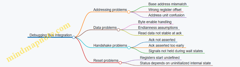
Example: A Minimal Bring-Up Test Strategy
Before adding interrupts or complex behavior, test only register reads and writes:
- Write a known pattern to
CTRLand read it back. - Confirm
STATUSchanges only when expected. - Perform at least one byte-enabled write if your software uses it.
This keeps the first failure localized: if reads work but writes don’t, the bug is in write handling; if neither works, the bug is likely in address mapping or bus attachment.
Summary
Adding peripherals with LiteX buses and Wishbone interconnect is mostly about disciplined mapping and correct bus semantics. Define clear register offsets, implement byte-aware writes, ensure ack timing is consistent, and validate with small, deterministic tests before layering on interrupts and higher-level functionality.
4.4 Building Boot Flow Components for FPGA Bring Up
A boot flow for an FPGA RISC-V SoC is mostly a choreography of small, predictable steps: set up the hardware state, load a program image, and confirm that the CPU and peripherals agree on what “memory” means. The goal is not to impress the simulator; it is to make the first successful instruction repeatable.
Boot Flow Components and Responsibilities
Think of the boot flow as four layers that hand off cleanly:
- Reset and clock discipline: ensure the CPU and interconnect see stable clocks and a synchronized reset release.
- Boot ROM or bootloader: provide an initial instruction stream and a way to locate the next stage.
- Memory initialization: set up RAM contents and any required data sections for the software runtime.
- Software runtime bring up: initialize stack, handle traps, and start the main program.
A practical best practice is to keep the first stage tiny and deterministic. If the first stage is too clever, you lose the ability to debug it with simple signals like UART prints and register reads.
Hardware Side: Reset, Boot Entry, and Image Placement
On FPGA, the most common failure mode is “the CPU started, but it started at the wrong place.” That can happen when the boot entry address does not match the memory map, or when the memory contents are not present when the CPU begins fetching.
A clean approach is:
- Define a single boot entry address in the SoC configuration and use it consistently in both hardware and software.
- Use a boot ROM for the earliest instructions. The ROM can be implemented as a small Verilog module or generated from a hex file.
- Place the next-stage image (or the full program) at a known RAM address, then let software copy or directly execute depending on your design.
If you use a ROM that jumps into RAM, you must ensure RAM is initialized before the jump. If you cannot guarantee that, keep the ROM self-contained for the first software stage.
Mind Map: Boot Flow from Reset to Main
Boot ROM Design Pattern with a Deterministic Jump
A minimal ROM should do two things: provide a known instruction stream and transfer control to the software entry point. In a LiteX-style SoC, the ROM can be mapped at the CPU’s reset vector or at a configured boot address.
Example boot ROM behavior:
- At reset, CPU fetches from ROM.
- ROM executes a jump to
software_entry. software_entryassumes RAM is ready and that the stack pointer is set by runtime code.
Here is a compact pseudo-structure of the ROM logic. The exact syntax depends on your HDL, but the idea is stable.
// Conceptual ROM wrapper
module boot_rom #(parameter BOOT_ADDR = 32'h0000_0000) (
  input  wire        clk,
  input  wire [31:0] cpu_pc,
  output wire [31:0] cpu_instr
);
  // ROM contents preloaded from a hex file
  // cpu_instr is selected based on cpu_pc
  // cpu_pc should match BOOT_ADDR mapping
endmodule
Software Side: Startup Code That Matches the Hardware Map
Hardware can only be “right” if software agrees with it. Your startup code should:
- Set the stack pointer to a valid RAM region.
- Initialize .data from ROM/flash image to RAM.
- Clear .bss to zero.
- Install a trap handler early enough that exceptions during init are visible.
A simple, effective debugging tactic is to print a single character over UART at each milestone: after stack setup, after data init, after trap handler install, and right before calling main. If you see the last character, you know exactly which step failed.
Example: UART Milestones for Boot Verification
In your startup routine, structure the code so each milestone is unambiguous:
uart_putc('A')after stack pointer setup.uart_putc('B')after.datacopy.uart_putc('C')after.bssclear.uart_putc('D')after trap handler install.uart_putc('E')right beforemain().
If the UART output stops at C, you focus on memory initialization rather than trap logic.
Advanced Details: Trap Vector and Exception Visibility
When bring up goes wrong, exceptions are often the first clue. Install a trap handler that:
- Reads
mcauseandmepc. - Optionally reads a few CSRs that help interpret the fault.
- Prints a short message over UART.
- Halts in a loop so the output remains stable.
Keep the handler simple. A handler that tries to do complex work can fail in the middle of reporting, leaving you with silence.
Integrated Checklist for FPGA Bring Up
- Boot entry address matches the SoC configuration.
- Boot ROM is mapped so the CPU fetches valid instructions immediately.
- RAM initialization strategy is consistent with the ROM jump timing.
- Startup code sets stack and initializes memory sections correctly.
- UART milestones confirm progress through each startup step.
- Trap handler prints
mcauseandmepcand then halts.
A boot flow that follows these rules tends to be boring in the best way: when something breaks, the failure is localized, and the next fix is obvious.
4.5 Verifying SoC Connectivity with LiteX Generated Artifacts
Connectivity bugs are usually boring: a wrong address, a missing bus bridge, a swapped interrupt line, or a peripheral that never sees valid bus cycles. LiteX helps because it generates artifacts that describe the SoC as built. The goal of this section is to turn those artifacts into a checklist you can execute, then into a small set of targeted tests that confirm the SoC behaves as the description claims.
Foundational Idea: Treat Generated Files as a Contract
LiteX emits multiple views of your design: a memory map, bus interconnect wiring, peripheral register layouts, and build-time parameters. Verification starts by assuming these files are the contract, then checking that your RTL and software agree with the contract.
A practical workflow looks like this:
- Confirm the SoC build artifacts exist and correspond to the same configuration you intend to test.
- Extract the memory map and interrupt wiring from the generated outputs.
- Validate that the bus interconnect routes transactions to the expected slaves.
- Run a minimal software test that touches each connectivity path.
- Compare observed behavior against the contract, not against guesses.
What to Look for in LiteX Artifacts
The exact filenames vary by project, but the content categories are consistent.
- Memory Map View: base addresses, region sizes, and register offsets per peripheral.
- CSR and Register Layout: CSR numbers, widths, and which CSRs are implemented.
- Interconnect Topology: which bus segments connect to which slaves, including bridges.
- Interrupt Wiring: which interrupt sources feed which CPU interrupt lines.
- Build Metadata: CPU type, clocking parameters, and SoC configuration hashes.
If any of these are missing, stop early. A missing memory map usually means your build did not include the peripheral you think it did.
Mind Map: Connectivity Verification Flow
Example: Memory Map Consistency Check
Suppose your UART peripheral is supposed to live at 0x4000_0000, and its control register is at offset 0x00. The contract says: UART_CTRL = 0x4000_0000 + 0x00.
A connectivity-first test writes a distinctive pattern to the control register, then reads it back. If the read returns a different value, you likely have one of these issues:
- software uses a different base address than the generated map,
- the peripheral is not actually connected to the bus segment you think it is,
- the register is write-only or has side effects that change the stored value.
To keep the test deterministic, choose a pattern that should not be transformed by the peripheral. For example, write 0x0000_00A5 and expect the same value on readback if the register is a plain storage register.
Example: Bus Routing and Bridge Presence
If your SoC uses a bus bridge between widths or protocols, the bridge is part of connectivity. A common failure mode is that the bridge exists, but the address decoder does not match the intended region.
A targeted check is to perform a read from the first address in the peripheral region and confirm it returns the expected default value (often zero). Then read from the last address in the region. If one end works and the other fails, the decoder boundaries are wrong or the region size in the contract does not match the implemented decoder.
Example: Interrupt Wiring Verification
Interrupt connectivity has two layers: the source asserts, and the CPU observes it.
Use a peripheral that can generate an interrupt from a software-visible action, such as a timer compare or a GPIO edge detector. The contract should specify:
- which interrupt number or line the peripheral drives,
- which status bit indicates the interrupt condition,
- how software clears the condition.
A minimal test sequence is:
- Enable the peripheral interrupt.
- Trigger the interrupt condition.
- Poll the CPU-visible status or read the peripheral status.
- Clear the interrupt condition.
- Confirm the interrupt does not immediately reassert.
If the CPU never sees the interrupt, check whether the peripheral’s interrupt output is connected to the correct CPU line in the interconnect topology. If the CPU sees it but it never clears, check the clear semantics in the register layout contract.
Diagram: Connectivity Contract to Test Mapping
    flowchart TD
  A[LiteX Generated Artifacts] --> B[Memory Map Contract]
  A --> C[Interconnect Topology]
  A --> D[Interrupt Wiring]
  B --> E[Software Address Touch]
  C --> F[Bus Routing Smoke Reads]
  D --> G[Interrupt Trigger and Clear]
  E --> H[Compare Observed vs Contract]
  F --> H
  G --> H
  H --> I[Per Peripheral Pass Fail]
Advanced Detail: Make Failures Actionable
When a check fails, record the smallest evidence set:
- the peripheral name,
- the contract addresses and offsets used,
- the exact register values read back,
- the interrupt line and status bits involved.
This turns “it doesn’t work” into “UART_CTRL readback differs from expected at address X,” which is the difference between hours of guessing and minutes of correction.
Practical Checklist for This Subsection
- Memory map regions do not overlap and match software constants.
- Each peripheral has a reachable bus path in the interconnect topology.
- Interrupt sources connect to the intended CPU line.
- Reset sequencing allows bus transactions after initialization.
- Minimal software tests cover readback, boundary addresses, and interrupt trigger/clear.
Once these checks pass, you can treat the SoC connectivity as verified at the level that matters: the contract in generated artifacts matches the behavior you can observe.
5. Designing Memory Maps and Bus Interconnects
5.1 Creating a Consistent Address Map Across CPU and Peripherals
A consistent address map is the quiet contract between your CPU, interconnect, and peripherals. If it is sloppy, you get symptoms like “UART works sometimes,” “interrupts fire at random,” or “software reads 0xFFFFFFFF and blames the hardware.” The goal here is to make the map predictable, aligned, and mechanically checkable.
Foundational Rules That Keep Everything Boring
Start with a few rules that you apply everywhere:
- Choose a base address per peripheral and never “reuse” ranges for convenience. If something moves, it moves once.
- Use power-of-two region sizes so address decoding is simple and errors are obvious.
- Align registers to their natural width (e.g., 32-bit registers on 4-byte boundaries). Misalignment forces extra logic and complicates software.
- Define register offsets in a single convention: for example,
0x00for control,0x04for status,0x08for data. Keep the pattern consistent across peripherals. - Reserve space for growth by leaving gaps inside each peripheral region. This prevents “address map archaeology” later.
A practical example: suppose you have a 32-bit SoC with memory-mapped IO. You might allocate:
- UART at
0x1000_0000with a 4 KiB region - GPIO at
0x1000_1000with a 4 KiB region - Timer at
0x1000_2000with a 4 KiB region - Interrupt controller at
0x1000_3000with a 4 KiB region
These are spaced by 0x1000, so decoding can be done by checking the upper address bits.
From Requirements to a Concrete Map
Work from the CPU’s perspective first:
- Address width and endianness: confirm what the CPU can generate and how bytes map to words.
- Access width: decide whether peripherals support byte, halfword, and word accesses or only word accesses.
- Atomicity expectations: if software will do read-modify-write, your register semantics must be clear.
Then translate into a map specification:
- For each peripheral, list
base,regionSize, and a table ofoffset -> registerName. - For each register, specify
resetValue,accessType(R, W, RW), and any special behavior (write-one-to-clear, read-to-pop, etc.).
A small but effective discipline is to keep the map in one place and generate both hardware decode constants and software headers from it. Even if you do not automate everything, using the same source reduces mismatches.
Decoding Strategy That Matches the Map
Your interconnect needs to route transactions based on address ranges. A simple and reliable approach is:
- Compute
regionIndex = (addr - globalIOBase) / regionSize. - Select the peripheral using
regionIndex. - Within the peripheral, decode
offset = addr % regionSize.
This approach keeps the interconnect logic consistent with the map’s power-of-two regions.
Example: UART Register Offsets
Assume UART region base 0x1000_0000 and region size 0x1000.
0x000TX register (write-only)0x004RX register (read-only)0x008STATUS register (read-only)0x00CCTRL register (read-write)
Software then uses absolute addresses like UART_TX = 0x1000_0000 + 0x000.
Mind Map: Address Map Consistency
Address Map Consistency Mind Map
Verification Checks That Catch Real Mistakes
Consistency is not just a design-time feeling; it is something you can test.
- Overlap checks: ensure no two peripherals’
[base, base+size)ranges intersect. - Decode coverage: in simulation, issue reads and writes to every defined register offset and confirm the peripheral responds.
- Unmapped behavior: define what happens for addresses outside all regions. For example, unmapped reads return
0x0and unmapped writes do nothing. Then test it. - Width handling: if your bus supports byte enables, test that writing a single byte updates only the intended bits.
Diagram: Address Routing Flow
    flowchart TD
  A[CPU generates address and access type] --> B[Interconnect range decode]
  B --> C{Address in UART region?}
  C -- Yes --> D[UART offset decode]
  C -- No --> E{Address in GPIO region?}
  E -- Yes --> F[GPIO offset decode]
  E -- No --> G{Address in Timer region?}
  G -- Yes --> H[Timer offset decode]
  G -- No --> I[Unmapped region handling]
  D --> J[Read data or write response]
  F --> J
  H --> J
  I --> J
A Quick Integrated Example Map
Here is a coherent mini-map that follows the rules above:
- Global IO base:
0x1000_0000 - UART: base
0x1000_0000, region0x10000x000TX (W)0x004RX (R)0x008STATUS (R)0x00CCTRL (RW)
- GPIO: base
0x1000_1000, region0x10000x000DATA (RW)0x004DIR (RW)0x008INT_EN (RW)0x00CINT_STAT (R/W1C)
With this structure, both hardware and software can agree on absolute addresses, decoding stays simple, and test cases can be written systematically by iterating over the register tables.
5.2 Handling Alignment Regions and Register Layout Conventions
A register map is only useful if software can predict where every bit lives and how it can be accessed. Alignment regions and layout conventions solve two practical problems: (1) keeping bus transactions simple and deterministic, and (2) preventing “works on my machine” bugs caused by mismatched assumptions about width, endianness, and access size.
Alignment Regions: What They Are and Why They Matter
An alignment region is a block of address space reserved for registers that share a common access granularity. For example, if your bus supports 32-bit reads and writes, you typically group registers into 4-byte slots. Within each slot, you may pack multiple smaller fields, but you still treat the slot as the atomic unit for bus transactions.
A good convention is:
- Use a fixed stride per register slot, commonly 4 bytes for 32-bit buses.
- Place each register at an address that is a multiple of its slot size.
- Keep multi-word registers (like 64-bit values) aligned to their total width, or at least aligned to the first word with a documented ordering.
This prevents partial-word accesses from becoming a guessing game. If software must read a 64-bit counter, it should do so using two 32-bit reads from a defined low-then-high order, or using a bus feature that supports atomic 64-bit accesses (if your platform provides it). Either way, the rule must be explicit.
Register Layout Conventions: Bit Positions and Access Semantics
Within a 32-bit slot, define fields with consistent bit numbering:
- Bit 0 is the least significant bit.
- Ranges are written as [hi:lo] with hi >= lo.
- Unused bits are reserved and should read as 0 unless your design has a reason to do otherwise.
Access semantics should be equally consistent:
- RW fields accept writes; RO fields ignore writes.
- W1C fields clear when a 1 is written; writing 0 leaves the bit unchanged.
- W1S fields set when a 1 is written.
- For “write-only” registers, still define what reads return (often 0) so software doesn’t interpret garbage.
When packing fields, avoid creating write hazards. A classic pitfall is a register where software writes only one field but the hardware interprets the entire 32-bit word. If you expect software to update individual fields, provide either:
- Separate registers per field, or
- A documented read-modify-write pattern in software, or
- Hardware-side masking so only the intended bits change.
A Systematic Addressing Scheme
Use a naming and addressing scheme that mirrors the hardware structure. A simple pattern is:
- Base address per peripheral.
- Register offsets in multiples of the slot size.
- Field offsets documented within each register.
Example: a UART-like peripheral with 32-bit slots.
- STATUS at offset 0x00
- CTRL at offset 0x04
- TXDATA at offset 0x08
- RXDATA at offset 0x0C
Even if STATUS only uses bits [3:0], it still occupies 0x00–0x03. That way, software never needs to know whether a field is “small”; it only needs to know the slot.
Multi-Word Registers and Ordering Rules
For 64-bit values stored as two 32-bit words, define ordering and consistency rules:
- Low word at offset N, high word at offset N+4.
- Software reads low then high, or high then low, but the choice must match the hardware’s capture behavior.
If the hardware updates the 64-bit value continuously, you may need a snapshot mechanism (for example, latching on a read of the high word). If you don’t, document that the two reads may observe different moments in time. The goal is not perfection; it’s predictability.
Mind Map: Alignment and Layout Rules
Example: Packing Fields Without Surprises
Suppose CTRL at 0x04 contains:
- [0] ENABLE (RW)
- [3:1] MODE (RW)
- [7:4] RESERVED (RO, read 0)
- [31:8] RESERVED (RO, read 0)
A safe write rule is: hardware updates only bits [3:0] and ignores the rest. Software can then write a full 32-bit word without needing to preserve reserved bits. If you cannot guarantee masking, then software must use read-modify-write, and your documentation must say so.
Example: 64-Bit Counter with Defined Read Behavior
Let COUNTER_LO at 0x10 and COUNTER_HI at 0x14.
- Software reads COUNTER_LO first, then COUNTER_HI.
- Hardware latches the 64-bit value when COUNTER_LO is read.
This makes the two reads consistent without requiring special bus support. The key is that both the latch trigger and the word order are written down as part of the register convention.
Practical Checklist for Implementation and Documentation
Before you move on, verify:
- Every register offset is aligned to the slot size.
- Every field has a defined [hi:lo] range.
- Every access type has explicit write and readback behavior.
- Every multi-word register has a documented word order and consistency rule.
- Reserved bits have a defined read value and a defined write policy.
With these conventions in place, your software can be boring in the best way: it reads and writes predictable addresses, and the hardware interprets those transactions consistently.
5.3 Implementing Register Interfaces with Read Write Semantics
Register interfaces are where “the CPU’s idea of a value” meets “the hardware’s idea of a signal.” A good implementation makes read and write behavior predictable, byte-accurate where needed, and safe under reset and bus stalls. This section focuses on practical semantics you can map directly onto LiteX-style bus transactions.
Core Semantics to Get Right
Start by defining what a register read returns and what a write changes. For each register, decide:
- Read value source: stored state, combinational status, or a mix.
- Write effect: full overwrite, masked update, or write-only behavior.
- Side effects: whether a write triggers an action (like clearing an interrupt) or only updates storage.
- Read-after-write behavior: whether the next read reflects the new value immediately or after a clock edge.
A simple rule keeps designs sane: writes update storage on the rising clock edge when the bus handshake completes. Reads sample either storage (registered) or status (combinational) at the time of the read handshake.
Address Decode and Transaction Handshake
In a memory-mapped SoC, the bus typically provides addr, wdata, we, strobe (byte enables), and a handshake like valid/ready or cyc/stb/ack. Your register block should:
- Decode
addrinto a one-hot register select. - Gate write updates with both the bus write enable and the handshake completion.
- Gate read data with the bus read handshake.
If your bus can issue back-to-back accesses, ensure your register block can respond every cycle or apply backpressure consistently. The easiest approach is to make read data purely combinational from the selected register and drive ack/ready in the same cycle as the request.
Read Data Construction
For each register, build a read value function:
- Storage-backed register:
rdata = reg_q. - Status register:
rdata = status_comb(often derived from counters, flags, or synchronizers). - Mixed register:
rdata = {status_bits, reg_q_bits}.
When mixing, be explicit about which bits are stable and which can change asynchronously. If a status bit crosses clock domains, synchronize it before exposing it to the bus.
Write Data with Byte Enables
Byte enables matter because software may write partial words. A robust pattern is:
- Split
wdatainto bytes. - For each byte lane, update only the corresponding bits.
This avoids accidental corruption of neighboring fields. It also makes it easier to implement “write only some bits” semantics without inventing new software rules.
Masked Field Updates
Often you want field-level control rather than whole-register overwrites. The clean approach is:
- Define a field mask for each writable field.
- Compute
next_field = (old_field & ~mask) | (new_field & mask).
This keeps unrelated bits stable. It also makes it easy to implement registers where some bits are read-only or reserved.
Side-Effect Registers and Clear-on-Write
Some registers behave like commands. A common example is a clear-on-write interrupt status register. Semantics:
- Reading returns the current pending bits.
- Writing a
1clears the corresponding pending bit. - Writing
0leaves it unchanged.
This is a masked update where the “mask” is the write data itself. Implement it by ANDing the pending state with the inverse of the write bits.
Reset Behavior and Determinism
Reset is not just “set everything to zero.” Decide which registers should reset to known values and which should reset to safe defaults. For example:
- Control registers: reset to a conservative configuration.
- Status registers: reset to zero unless hardware requires otherwise.
- Command/clear registers: reset to zero because they are storage-backed only for pending flags.
Determinism helps debugging: when software reads a register after reset, it should see the same values every time.
Example: Two Registers with Different Semantics
Below is a compact register block sketch. It assumes a 32-bit bus with byte enables and a single clock domain.
// reg block: one storage reg and one clear-on-write pending reg
reg [31:0] ctrl_q;
reg [31:0] pending_q;

wire sel_ctrl    = (addr == 32'h0000_0000);
wire sel_pending = (addr == 32'h0000_0004);
wire do_write    = bus_we & bus_ack; // handshake completion
wire [3:0] be    = bus_strobe;

// byte-lane mask from strobe
wire [31:0] be_mask = { {8{be[3]}}, {8{be[2]}}, {8{be[1]}}, {8{be[0]}} };

always @(posedge clk) begin
  if (rst) begin
    ctrl_q    <= 32'h0000_0000;
    pending_q <= 32'h0000_0000;
  end else begin
    if (do_write && sel_ctrl) begin
      ctrl_q <= (ctrl_q & ~be_mask) | (bus_wdata & be_mask);
    end
    if (do_write && sel_pending) begin
      // clear-on-write: writing 1 clears that bit
      pending_q <= pending_q & ~bus_wdata;
    end
  end
end

assign bus_rdata = sel_ctrl ? ctrl_q :
                    sel_pending ? pending_q :
                    32'h0000_0000;
This example highlights three practical choices: storage updates only on handshake completion, byte enables gate the control register update, and the pending register uses write data as a bitwise clear mask.
Mind Map: Register Interface Read Write Semantics
Practical Checklist for Implementation
Before you wire the block into the SoC, verify these points in simulation:
- A write changes only the intended bits, including under partial byte enables.
- A clear-on-write register clears exactly the written
1bits. - Reads return the expected values during and after reset.
- Unmapped addresses return a defined value (often zero) and do not accidentally update state.
When these are correct, the rest of the system—software bring-up, interrupt handling, and bus-level debugging—becomes much less mysterious.
5.4 Managing Interrupt Lines and Status Registers
Interrupts are where “it works in simulation” meets “why is the board silent.” A clean interrupt design makes three things explicit: which source can request an interrupt, how the CPU learns which source is pending, and how software clears the condition without accidentally losing events.
Foundational Model of Interrupts
Start with a simple mental model: each interrupt source produces an interrupt request signal, the SoC aggregates requests into one or more interrupt lines, and the CPU samples those lines to set pending bits in its interrupt controller view.
In a typical RISC-V setup, software observes interrupt state through CSRs (like mstatus, mie, and mip) and uses mcause to learn why it trapped. Hardware must ensure that:
- The interrupt request is synchronized to the CPU clock domain.
- Pending state is latched long enough for the CPU to notice.
- Clearing is deterministic and tied to either a software action or a hardware condition.
A practical best practice is to treat each interrupt source as having two signals: irq_req (request) and irq_clr (clear). Even if your bus protocol doesn’t expose irq_clr directly, you can implement it internally.
Status Registers That Software Can Trust
Status registers serve two jobs: they tell software what happened, and they provide a controlled way to clear it. A common pattern is a per-source register with:
- A
pendingbit that is set by hardware when an event occurs. - A
enablebit that gates whether the interrupt request is asserted. - A
clearmechanism that software can trigger without guessing.
For example, a timer peripheral might expose TIMER_IRQ_STATUS with bits pending and enable. Hardware sets pending when the timer reaches the compare value. Software clears pending by writing a 1 to a clear bit (write-one-to-clear, W1C). This avoids the ambiguity of “write zero to clear” when bus writes might be partial.
Aggregating Interrupt Lines in LiteX SoCs
When multiple peripherals request interrupts, the SoC must combine them. The simplest approach is OR-ing request lines into a single interrupt input, but that only works if the CPU can still identify the source. In practice, you pair aggregation with status registers so software reads the peripheral status to determine which one is pending.
A robust approach is:
- Each peripheral produces a latched
pendingbit. - Each peripheral asserts
irq_req = pending & enable. - The SoC ORs all
irq_reqsignals into the CPU interrupt input. - Software reads each peripheral’s status to find which
pendingbits are set.
This keeps the CPU-side logic simple and pushes source identification into readable registers.
Example Register Behavior for One Interrupt Source
Consider a UART receive interrupt. The peripheral sets rx_pending when a byte arrives and the receive FIFO is non-empty. Software enables the interrupt with rx_enable.
- Hardware:
rx_pendingset on receive event. - Interrupt request:
uart_irq_req = rx_pending & rx_enable. - Clearing: when software reads the RX data register until FIFO is empty, hardware clears
rx_pending.
If you prefer explicit clearing, add rx_pending_w1c and clear on a write. Either way, document the rule so software doesn’t clear too early.
Mind Map of Interrupt and Status Design
Mind Map: Interrupt Lines and Status Registers
Advanced Details That Prevent Subtle Bugs
Synchronization: If a peripheral runs on a different clock, synchronize irq_req or, better, synchronize the event that sets pending. Synchronizing only the request can cause missed edges if the request pulses briefly.
W1C vs level-clear: W1C is safer with bus writes because software can clear exactly what it intends. Level-clear is simpler but requires software to perform the right sequence (like draining a FIFO) before the interrupt disappears.
Partial writes: If your bus supports byte enables, ensure your clear logic respects them. A write that only updates the lower byte should not accidentally clear the entire register.
Read-modify-write hazards: Avoid designs where software must read a status register, modify it, and write it back to clear bits. Prefer W1C or separate clear registers.
Minimal RTL Sketch for Pending and Clear
This sketch shows the core idea: latch pending, gate with enable, and clear deterministically.
// irq_pending: latched by event
// irq_enable: set by software
// irq_clear_w1c: asserted when software writes 1 to clear bit
always_ff @(posedge clk) begin
  if (rst) begin
    irq_pending <= 1'b0;
    irq_enable  <= 1'b0;
  end else begin
    if (event_pulse) irq_pending <= 1'b1;
    if (irq_clear_w1c) irq_pending <= 1'b0;
    if (enable_write) irq_enable <= enable_write_data;
  end
end

assign irq_req = irq_pending & irq_enable;
Example Software Service Routine Logic
Software should follow a predictable order:
- Check the CPU trap cause to confirm it is an interrupt.
- Read peripheral status registers to find which
pendingbits are set. - Service the corresponding condition (read FIFO, acknowledge hardware, or perform the required action).
- Clear the pending bits using the documented mechanism.
If you clear before servicing, you risk losing the evidence needed to complete the operation. If you service before clearing, you avoid that risk, but you must ensure the clear condition won’t be blocked by stale state.
Validation Checklist for Interrupt Correctness
- Trigger an interrupt source and confirm the CPU observes it.
- Confirm the peripheral
pendingbit remains set until the clear rule is satisfied. - Confirm that disabling
enableprevents further interrupt requests while pending may still be readable. - Confirm that multiple sources can be pending simultaneously and software can identify each one.
- Confirm that partial bus writes do not clear unintended bits.
A well-behaved interrupt system is mostly about boring determinism: pending latches, clear rules, and software-readable status. Once those are consistent, the rest of the bring-up story becomes much less mysterious.
5.5 Validating Bus Transactions With Deterministic Testbenches
A deterministic bus testbench checks that every request produces the expected response, cycle by cycle, without relying on timing luck. The goal is simple: if the RTL changes, the test should fail for the right reason, not because the test itself is flaky.
Foundations: What “Deterministic” Means
Determinism comes from three choices. First, you drive inputs from a fixed schedule (explicit cycles or explicit handshakes). Second, you model expected outputs with the same handshake rules the bus uses. Third, you log enough information to pinpoint the first mismatch.
Start by defining the bus contract in plain terms: which signals indicate request validity, which indicate readiness, and what counts as a completed transaction. For a typical ready/valid bus, a transfer happens only when both sides agree in the same cycle. Your testbench should treat that as the only “real” event.
Mind Map: Deterministic Bus Validation
Building Blocks: Stimulus, Model, Scoreboard
A deterministic testbench usually has three layers.
-
Stimulus generator: produces a sequence of bus operations. Keep it small at first: a few reads and writes to known addresses. Use a fixed order and fixed values.
-
Reference model: predicts what the bus should return. For register-mapped peripherals, the model can be a dictionary from address to register value plus rules for side effects.
-
Scoreboard: matches observed responses to expected ones. The scoreboard is where determinism pays off: it should not “guess” which response belongs to which request.
If the bus supports multiple outstanding transactions, you need a matching key. If it does not, you can enforce in the test that only one request is in flight at a time. Either way, the scoreboard must define the matching policy explicitly.
Example: Register Read Write with Byte Enables
Assume a 32-bit bus with byte enables be[3:0]. A write updates only the selected bytes. Your reference model should apply a mask.
Example scenario:
- Write
0x11223344to address0x1000withbe = 1111. - Read back from
0x1000and expect0x11223344. - Write
0xAABBCCDDto the same address withbe = 0010(only byte 1). - Read back and expect only that byte changed.
The testbench should compute the expected value using the same byte ordering as the RTL. A common mistake is swapping endianness in the mask application; the read-after-write check catches it immediately.
Protocol Assertions That Catch Real Bugs
Deterministic tests are stronger when paired with assertions. Add checks that enforce the bus contract, not the peripheral behavior.
- Transfer definition: if
valid && readyis false, the scoreboard must not advance. - Stability: when
validis high butreadyis low, request fields like address and write data must remain stable. - No phantom responses: response valid must not appear without a corresponding expected request.
These assertions reduce the chance that your test passes while the RTL violates the handshake.
Scoreboard Matching Rules
A practical scoreboard approach:
- Enqueue each expected request when you observe the request transfer.
- When a response transfer occurs, pop the oldest expected request and compare fields.
- If the response arrives early or late, fail with a message that includes the cycle number and the mismatched transaction.
This “first in, first out” policy is correct for buses that serialize requests. If the bus allows reordering, you must match using an explicit tag or by reconstructing ordering rules from the protocol.
Advanced Details: Alignment, Side Effects, and Backpressure
Once basic reads and writes pass, add the cases that break naive models.
- Alignment: if the bus allows unaligned accesses, define how the peripheral handles them. If it forbids them, assert that the RTL returns an error or ignores the access according to the spec.
- Side effects: some registers clear on read or trigger on write. Your reference model must implement those rules so that the second access behaves correctly.
- Backpressure: deterministic backpressure still can be systematic. Instead of random stalls, drive
readylow on a predetermined pattern (for example, every 5th cycle) and verify that the RTL holds request fields stable and completes transactions only when allowed.
Debugging Output That Makes Failures Actionable
When a mismatch occurs, print:
- cycle number
- request address and type (read/write)
- expected vs observed data
- whether the mismatch is in the request phase or response phase
This is enough to reproduce the issue without drowning in logs. The first failure should be the only one that matters; later mismatches are often just consequences.
Minimal Deterministic Test Sequence
Use a short, ordered sequence that covers the core contract:
- Write full word to a register.
- Read it back.
- Write with byte enables.
- Read back again.
- Apply a predetermined backpressure pattern.
- Confirm no phantom responses and no missing responses.
If this passes, your testbench is likely deterministic and your reference model is aligned with the RTL’s handshake and data rules. After that, expand coverage by adding side-effect registers and error paths.
6. Verilator Simulation for Fast RTL Verification
6.1 Setting Up Verilator for Chisel Generated Verilog
Verilator turns your generated Verilog into a fast cycle-accurate simulation model. The setup is mostly about making sure the generated design and your testbench agree on clocks resets and interface timing. The goal is simple: run a repeatable simulation that fails loudly when something is wrong.
Mind Map: Verilator Setup Flow
Step 1: Choose the Simulation Top Module
Chisel can emit multiple modules, but Verilator needs one top-level module for elaboration. In practice, you pick either:
- Your SoC top module (and provide a testbench that drives its external pins), or
- A wrapper that instantiates the SoC and exposes a clean set of testbench-visible signals.
A common best practice is to create a small wrapper module so you control reset sequencing and clock generation without touching the generated SoC. This also keeps Verilator’s “what is the top?” decision stable even if the SoC internals change.
Step 2: Generate Verilog and Keep the Build Inputs Deterministic
Chisel generation should produce a fixed set of Verilog files for a given configuration. Treat the generated output directory as an input artifact: don’t mix multiple configurations in the same folder. When you run Verilator, point it at the exact generated Verilog paths and the exact testbench sources.
If your SoC uses parameters, ensure the Verilog is generated with those parameters baked in, or pass matching -G values to Verilator. Mismatched parameters are a classic source of “it compiles but behaves strangely.”
Step 3: Pick Verilator Options That Match Your Debug Needs
Start with a conservative set of options, then add features only when needed.
--ccconverts Verilog to C++.--exetells Verilator you have a C++ testbench.--buildcompiles and links in one go.--traceenables waveform dumping (useful for bus timing and reset issues).--timinghelps when you care about delays or want more accurate ordering.
Also decide whether to treat warnings as errors. For bring-up, it’s often better to fail on serious issues early, but don’t turn every warning into a hard error until you’ve cleaned up the baseline.
Example: Minimal Verilator Command for a Wrapper Top
verilator --cc --exe --build \
  --trace \
  -Wno-fatal \
  -I obj_dir \
  -I tb \
  --top-module TbTop \
  obj_dir/TopSoC.v \
  tb/TbTop.cpp tb/TbTop.v
This assumes:
TbTopis your wrapper top module.TopSoC.vis the generated Verilog file.TbTop.cppdrives the simulation.TbTop.vprovides any Verilog-side glue if needed.
Step 4: Write a Testbench That Controls Clock and Reset
Verilator doesn’t magically know your reset behavior. Your C++ testbench should:
- Assert reset for a known number of cycles.
- Deassert reset on a clock edge.
- Run a fixed number of cycles per test.
A reliable pattern is to toggle the clock, evaluate the model, then apply stimulus on a consistent phase. If your design samples inputs on rising edges, apply inputs before the rising edge.
Example: Cycle Stepping Skeleton
for (int cycle = 0; cycle < maxCycles; cycle++) {
  tb->clk = 0;
  tb->eval();

  if (cycle == resetCycles) tb->reset = 0;

  tb->clk = 1;
  tb->eval();

  // Apply stimulus for next cycle here
  // Drive bus signals before the next rising edge
}
This structure keeps the “when do signals change” rule consistent. If you later add a bus driver, keep it aligned with this phase convention.
Step 5: Confirm Interface Timing with Small, Focused Checks
Before running a full software bring-up, validate the interface timing with tiny tests:
- A reset-only test that ensures no X-propagation surprises.
- A single transaction test that checks one read or write handshake.
- A CSR access test that confirms the expected response latency.
When a test fails, waveform traces should show the exact cycle where the handshake went wrong. If you don’t enable --trace, you’ll end up guessing, and guessing wastes time.
Step 6: Triage Lint and Elaboration Warnings
Verilator warnings often point to real issues: width mismatches, unused signals, or implicit truncation. Treat the first run as a baseline report. Fix the highest-signal warnings first, then rerun. Once the baseline is clean, you can re-enable stricter warning handling.
A practical rule: if a warning appears every run, it’s not “noise.” Either it’s harmless in your design context, or it’s a bug waiting for a specific stimulus.
Step 7: Automate the Command So You Don’t Rebuild Your Mistakes
Wrap the Verilator invocation in a script or Make target that records:
- The generated Verilog directory
- The chosen top module
- The test name
- The Verilator options
Automation doesn’t just save keystrokes; it prevents subtle mismatches between what you think you ran and what you actually ran.
6.2 Writing Cycle Accurate Testbenches for Bus and Peripheral Logic
Cycle accurate testbenches treat time as a first-class input. Instead of checking only “eventually correct” outputs, you verify that signals change on the expected clock edges, that handshakes obey their rules, and that bus transactions complete without hidden stalls. The payoff is simple: when something breaks, you know whether it broke early, late, or never.
Foundations for Cycle Accurate Thinking
Start by defining what “cycle accurate” means for your design. For a bus like Wishbone, you typically care about when cyc and stb are asserted, when ack is raised, and whether we, sel, and adr remain stable during the request phase. For a peripheral, you care about how it samples bus signals and when it updates internal state.
A useful mental model is a small timeline per transaction:
- Request phase: master asserts address and control.
- Wait phase: master holds stable signals while the slave is busy.
- Acknowledge phase: slave asserts
ackand providesrdataif it is a read. - Response cleanup: master deasserts request signals.
Cycle accurate tests should explicitly model these phases rather than relying on “one cycle later” assumptions.
Mind Map: Cycle Accurate Testbench Responsibilities
Building Blocks: Clock, Reset, Driver, Monitor
-
Clock and reset: Drive a free-running clock and apply reset for a fixed number of cycles. Deassert reset on a known edge so your first transaction begins from a clean state.
-
Bus driver: Implement a function that performs a single read or write by stepping cycle-by-cycle. The driver should:
- Assert
cycandstbwith stableadr,we,sel, andwdata. - Wait until
ackbecomes high. - Record the cycle index when
ackoccurs. - Deassert
cycandstbafter the acknowledge.
- Assert
-
Bus monitor: Continuously check invariants. For example, during the request and wait phases,
adr,we,sel, andwdatashould not change. If they do, the test should fail immediately with a cycle-stamped message. -
Peripheral checks: After each transaction, verify the peripheral’s externally visible behavior. For register blocks, this usually means reading back values and checking that write strobes affect only the intended bytes.
Example: A Cycle Accurate Wishbone Read Driver
The following pseudocode shows the structure. The key idea is that the driver advances one cycle at a time and asserts expectations at specific edges.
function wb_read(adr):
  drive adr
  drive we=0, sel=all_ones
  drive cyc=1, stb=1
  while ack==0:
    assert adr stable
    step one clock
  capture rdata
  capture ack_cycle
  step one clock
  drive cyc=0, stb=0
  return rdata, ack_cycle
A real testbench should also check that ack is not asserted spuriously when cyc and stb are low.
Example: Register Write with Byte Enables
For a peripheral register with byte lanes, you want to verify that partial writes update only selected bytes. A good test sequence is:
- Write
0x11223344to the register with all byte enables. - Write
0x0000AA00with only the middle byte enable asserted. - Read back and confirm the register becomes
0x1122AA44.
Cycle accuracy matters here because the peripheral must sample wdata and sel on the correct clock edge when the bus acknowledges.
Advanced Details That Prevent “False Passes”
-
Ack timing constraints: If your slave is designed to respond in exactly one cycle after a request, assert that
ackoccurs at the expected cycle. If it can stall, assert bounds like “ack must occur within N cycles.” -
Back-to-back transactions: Test consecutive reads or writes without inserting extra idle cycles. Many bugs show up only when the master changes signals immediately after an acknowledge.
-
Reset edge cases: Attempt a transaction right after reset deassertion. If your design requires a minimum idle cycle, encode that requirement explicitly in the test.
-
Invariant assertions: Keep monitors running for the entire simulation. Examples include “no X-propagation in critical control signals” and “ack implies cyc and stb were high in the same cycle.”
Mind Map: What to Assert per Cycle

Putting It Together: A Systematic Test Flow
A practical flow is: initialize, run a small set of deterministic transactions, then add targeted corner cases. For instance, start with a write-read pair to confirm basic connectivity, then test partial writes, then test back-to-back operations, and finally test a stall scenario by using a peripheral mode that delays acknowledge. Each step should include cycle-stamped checks so failures point to the exact phase where behavior diverged.
When your testbench is cycle accurate, you stop arguing about “what probably happened” and start recording “what happened on cycle K.” That’s the difference between debugging and guessing.
6.3 Using Assertions and Coverage for Interface Correctness
Interface correctness is where “it simulates” quietly turns into “it works on hardware.” Assertions and coverage in Verilator help you catch mismatched assumptions early: wrong handshake behavior, illegal register accesses, and bus timing mistakes that only show up after integration.
Foundations: What You Can Assert
Start with properties that are local to the interface signals. In a typical LiteX-style bus, you can assert rules like:
- Handshake stability: when
validis high andreadyis low, address and control must not change. - Single-cycle pulses: certain strobes must be one-cycle wide.
- No X-propagation in simulation: signals should not take unknown values at key boundaries.
A practical approach is to write assertions at the module boundary where the interface is “owned.” If a peripheral owns the response channel, assert response rules inside the peripheral wrapper, not in the SoC top.
Coverage: Measuring What You Actually Tested
Assertions answer “did this rule ever break?” Coverage answers “did we ever exercise the rule’s interesting cases?” Use coverage to ensure you hit:
- Both read and write paths.
- Boundary addresses in the memory map.
- Backpressure scenarios where
readyis deasserted. - Error paths such as unmapped addresses or misaligned accesses.
Coverage is not about quantity; it’s about hitting the decision points that assertions care about.
Mind Map: Interface Assertions and Coverage
Example: Handshake Stability for a Simple Bus
Assume a bus where a master drives addr, we, wdata, and valid, while the slave returns ready and later rdata with resp_valid. The master must keep request fields stable until the handshake completes.
// Pseudocode style assertions for a request channel
// Trigger on rising clock
always @(posedge clk) begin
  if (!reset_n) begin
    // During reset, avoid asserting protocol signals
    assert(!req_valid);
  end else begin
    if (req_valid && !req_ready) begin
      assert(req_addr == $past(req_addr));
      assert(req_we   == $past(req_we));
      assert(req_wdata == $past(req_wdata));
    end
    if (req_valid && req_ready) begin
      // Handshake completed; next cycle may change
      assert($stable(req_valid) == 0 || req_valid == 0 || 1);
    end
  end
end
In practice, keep assertions tight and readable. If you can’t explain the property in one sentence, it’s probably too broad.
Example: Coverage for Backpressure and Boundary Addresses
Coverage should mirror the assertions. If you assert stability under backpressure, you need coverage that proves you actually created backpressure.
// Pseudocode coverage counters
always @(posedge clk) begin
  if (reset_n) begin
    if (req_valid && !req_ready)
      cov_backpressure_stall <= cov_backpressure_stall + 1;

    if (req_valid && req_ready && req_addr == BASE_ADDR)
      cov_hit_base <= cov_hit_base + 1;

    if (req_valid && req_ready && req_addr == BASE_ADDR + SIZE - 4)
      cov_hit_last_word <= cov_hit_last_word + 1;

    if (req_valid && req_ready && req_addr[ADDR_W-1:2] == UNMAPPED_TAG)
      cov_hit_unmapped <= cov_hit_unmapped + 1;
  end
end
When coverage is missing, it usually means your testbench never created the conditions the assertion expects. Fix the stimulus first, not the assertion.
Advanced Details: Reset, Ordering, and Response Rules
Once the basic handshake is covered, move to ordering and response legality.
- Reset constraints: after reset deasserts, require that interface outputs settle before the first valid transaction. This prevents “first transaction is random” bugs.
- Response ordering: if the interface is single outstanding, assert that a new request cannot arrive until the previous response is observed.
- Error behavior: if unmapped addresses must return a specific error response, assert that the error code matches and that
rdatais either zeroed or marked invalid.
A common mistake is asserting too many things at once. Start with one property per failure mode: handshake stability, then response ordering, then error semantics.
Workflow: From Failing Assertion to Confident Interface
- Add one assertion for a single rule.
- Add one coverage point that proves the rule’s key scenario occurred.
- Run the existing regression and fix the first failure.
- Only after the failure is resolved, add the next rule.
This keeps the feedback loop short and prevents “assertion whack-a-mole,” where you keep changing properties without improving test quality.
6.4 Debugging Waveforms and Interpreting Simulation Results
When a simulation fails, the waveform is your map, not your destination. The goal is to convert signal motion into a concrete hypothesis about what the design believed at each cycle. Start with a small set of signals that answer the same questions every time: what transaction was attempted, what the bus expected, what the peripheral did, and whether the CPU observed the result.
1) Build a Debug Checklist Before You Look
Pick a “minimum viable trace” so you don’t drown in signals.
- Clock and reset: confirm reset deassertion timing and whether any logic is still in reset when activity begins.
- Bus handshake: for ready/valid style, capture
valid,ready, andaddr/wdata/rdataplusweorstrb. - Transaction identifiers: if the design has tags, include them; if not, use address and write/read direction.
- Peripheral state: include the state register(s) that gate behavior (e.g., UART TX state, timer compare latch, register file write enable).
- CPU-visible signals: include the bus response (
ackorrvalid) and any error flags.
A good habit: annotate the waveform with cycle numbers and mark the first cycle where the expected handshake should occur. Most bugs show up as “the first wrong belief,” not as a later symptom.
2) Read Waveforms as a Timeline of Beliefs
Treat each cycle as a snapshot of intent and outcome.
- If a master asserts
validbut the slave never assertsready, the master is waiting. That’s usually an interconnect or address decode issue. - If
readyis high but the master never assertsvalid, the master logic isn’t generating the request. That points to address generation, CSR side effects, or software expectations. - If both handshake, but the data is wrong, focus on the peripheral’s register mapping, byte enables, and alignment.
- If the handshake happens but the CPU still reports an exception or wrong value, the issue may be response timing: the peripheral might be returning data too early, too late, or for the wrong transaction.
A waveform that “looks busy” can still be correct. The trick is to compare what the design should have done on each handshake against what it actually did.
3) Mind Map for Systematic Debug Flow
Mind Map: Debugging Waveforms
4) Common Waveform Patterns and What They Mean
Pattern A: Handshake Never Completes
- Symptom:
validstays high,readystays low. - Likely causes: address decode mismatch (wrong base address), peripheral not enabled, or interconnect arbitration stuck.
- Example: a register at
0x1000_0008is expected, but the peripheral is mapped at0x1000_0010. The CPU will keep requesting the unmapped region, and the slave will never respond.
Pattern B: Handshake Completes, Data Is Stable but Wrong
- Symptom:
rvalid/ackoccurs, butrdatadoesn’t match. - Likely causes: incorrect register index calculation, endianness confusion, or byte-enable handling.
- Example: software writes a 32-bit value with byte enables, but the RTL ignores
strb. The waveform shows correct address and handshake, yet only some bytes change.
Pattern C: Data Changes During a Read Response
- Symptom:
rdatatoggles after the response is asserted. - Likely causes: combinational read paths without proper latching, or missing pipeline registers.
- Example: a register file read is modeled combinationally, but the bus expects registered output. The CPU samples
rdataon the response cycle, and the waveform reveals thatrdatais still settling.
Pattern D: Reset Timing Creates a One-Cycle Ghost
- Symptom: first transaction after reset returns zeros or X-like values.
- Likely causes: reset deassertion not synchronized to the bus clock, or peripheral state not initialized.
- Example: UART baud counter starts counting one cycle late, so the first TX bit timing is off. The waveform shows correct software writes, but the peripheral state machine enters the wrong phase.
5) A Concrete Example Walkthrough
Suppose a UART status register read should return 0x0000_0001 (TX ready). In the waveform:
- Cycle 120: CPU asserts a read request with address
0x2000_0004andvalid=1. - Cycle 121: UART slave asserts
ready=1; handshake completes. - Cycle 121:
rdatais0x0000_0000. - Cycle 122:
rdatabecomes0x0000_0001.
This indicates a response timing mismatch: the UART status logic updates one cycle after the bus samples it. The fix is to register the status value at the correct time or align the peripheral response with the bus handshake. The key evidence is the one-cycle shift between when the status becomes correct and when the bus response is asserted.
6) Use Assertions to Turn Waveforms into Evidence
Waveforms are great for humans; assertions are great for repeatability. Add checks that match the bus contract.
- Handshake contract: when
valid && ready, the address and control must be stable. - Response contract: when a read response is asserted,
rdatamust match the expected register value for that address. - Reset contract: during reset, outputs must be in known states.
Even a small set of assertions reduces the time spent scrolling, because the simulator points you to the first cycle where the contract breaks.
7) Interpret Results Without Getting Lost
When you see a mismatch, avoid the temptation to “fix the nearest thing.” Instead, identify the earliest divergence between expected and observed behavior. Then decide whether the divergence is in:
- Request generation (CPU/master side)
- Address decode and routing (interconnect/peripheral selection)
- Data path and register semantics (peripheral logic)
- Timing alignment (pipeline and handshake response)
Once you can label the divergence category, the waveform stops being a mystery and becomes a checklist with one failing item.
6.5 Automating Regression Runs with Make or Scripted Flows
Regression automation is about making the “same test, same inputs, same checks” happen reliably, even when you change RTL, software, or build options. The goal is not speed for its own sake; it’s repeatability with enough structure that failures are easy to interpret.
Foundational Principles for Regression Automation
Start by separating concerns:
- Build: generate Verilog, compile simulation, synthesize if needed, and package artifacts.
- Run: execute simulations or hardware tests with fixed parameters.
- Check: compare outputs against expected results and decide pass or fail.
- Report: collect logs, summaries, and the exact command lines used.
A practical rule: every regression run should be reproducible from a single command, with all variable inputs captured in a log file.
Mind Map: Regression Flow Components
Regression Automation Mind Map
Makefile Structure That Scales
A clean Makefile usually has phony targets for orchestration and real targets for files. Use variables to avoid copy-paste drift.
Key practices:
- Use a single test driver: one script or one make target that runs a test by name.
- Write outputs to per-test directories:
out/<test>/so logs don’t overwrite each other. - Use
-jsafely: parallel builds are fine; parallel runs require unique output paths. - Fail fast on build errors: don’t start runs if compilation fails.
Example Makefile skeleton:
TESTS := boot_smoke csr_smoke uart_smoke
OUTDIR := out
VERILATOR := verilator

.PHONY: all build regress clean
all: regress

build:
	./scripts/build_verilog.sh
	./scripts/build_sim.sh

regress: build
	@mkdir -p $(OUTDIR)
	@for t in $(TESTS); do \
		$(MAKE) run TEST=$$t || exit 1; \
	done

run:
	@mkdir -p $(OUTDIR)/$(TEST)
	@./scripts/run_test.sh $(TEST) $(OUTDIR)/$(TEST)

clean:
	rm -rf $(OUTDIR)
Scripted Flow for Deterministic Runs
When you need richer logic than Make provides, keep Make as the entry point and move the run logic into scripts. The script should:
- Validate arguments (test name, output directory).
- Set environment variables used by the testbench.
- Run the simulator with fixed options.
- Capture logs and exit codes.
- Run a checker that produces a single verdict file.
A minimal run script pattern:
#!/usr/bin/env Bash
set -euo pipefail
TEST="$1"
OUT="$2"

LOG="$OUT/run.log"
VERDICT="$OUT/verdict.txt"

mkdir -p "$OUT"

echo "Running $TEST" | tee "$LOG"

# Example: Verilator Simulation Invocation
./obj_dir/Vtb_$TEST +seed=1 +timeout=200000 \
  > "$OUT/stdout.txt" 2> "$OUT/stderr.txt" || true

./scripts/check_test.sh "$TEST" "$OUT" > "$VERDICT"
cat "$VERDICT"

if ! grep -q "PASS" "$VERDICT"; then
  exit 1
fi
Checkers That Make Failures Actionable
A checker should not just say “failed.” It should produce a small, consistent set of fields, such as:
- Observed signature (e.g., last PC, UART line count, CSR value)
- Expected signature
- Mismatch reason (missing token, wrong value, timeout)
For example, check_test.sh can parse a known marker printed by the testbench, like TEST_DONE signature=0x....
Regression Selection and Test Manifests
Avoid hardcoding test lists in multiple places. Instead, keep a manifest file that maps test names to options.
Example manifest idea:
tests/manifest.txtboot_smoke seed=1 waves=0csr_smoke seed=7 waves=0uart_smoke seed=3 waves=1
Your runner reads the manifest and runs tests in a stable order. Stable order matters when you compare logs across runs.
Practical Reporting and Artifact Preservation
At the end of a regression, write a summary file like out/summary.txt containing one line per test:
- test name
- PASS/FAIL
- runtime (if available)
- path to verdict and logs
When a test fails, preserve its output directory and stop the regression if you want quick feedback, or continue if you want a full failure list. Either way, the decision should be explicit in the command you run.
Advanced Details Without Overcomplication
- Timeouts: enforce them per test so a hung simulation doesn’t stall the whole run.
- Wave dumps: enable waves only for selected tests to keep disk usage predictable.
- Exit codes: treat nonzero exit codes as failures unless the checker confirms a known “expected” condition.
- Environment capture: log key variables (build options, seed, image hash) into the run directory so you can trace what happened.
A good regression command looks boring: one line, one output folder, and a summary that tells you exactly which tests failed and where to look. That’s the whole point.
7. Building a Bare Metal Software Stack for Bring Up
7.1 Selecting a Toolchain and Creating a Minimal Runtime
A minimal runtime is the smallest software layer that can boot, talk to at least one peripheral for visibility (usually UART), and run a few deterministic tests. The trick is choosing a toolchain that matches your hardware assumptions: ABI, ISA extensions, memory map, and the exact way your SoC starts executing.
Toolchain Selection Criteria
Start with the CPU and ABI your LiteX SoC expects. For RISC-V, that typically means RV32 or RV64, an ABI like ilp32 or lp64, and a set of extensions such as m, a, and sometimes c. If your hardware omits an extension, your compiler must not generate instructions that rely on it.
Next, align the linker script with your memory map. Your SoC’s ROM/RAM addresses and the location of the UART registers determine where code and data must live. A minimal runtime usually places:
.textin executable memory (often RAM for FPGA bring-up).rodatafor constants and strings.dataand.bssin RAM with a known zeroing strategy- a small stack region with a defined top-of-stack symbol
Finally, confirm the startup model. Some flows use a hardware reset vector that jumps to a C entry point; others expect a hand-written assembly _start that sets up stack and clears .bss. Your runtime should match the reset behavior your SoC actually implements.
Minimal Runtime Components
A practical minimal runtime has four parts:
- Startup code: sets
sp, initializes.bss, and callsmain. - System call stubs: often just UART output and a minimal
exitbehavior. - UART driver: a tiny write routine that polls a status bit and writes a byte.
- Test harness: a loop that prints progress and runs a few checks.
Keep the runtime small enough that you can reason about every instruction it emits. When something fails, you want the failure mode to be obvious: wrong address, wrong ABI, missing extension, or incorrect reset entry.
Mind Map: Toolchain and Runtime Building Blocks
Example: A Minimal UART-Backed main
This example assumes you have a memory-mapped UART with a status bit indicating transmit readiness.
#include <stdint.h>

#define UART_BASE 0x10000000UL
#define UART_TXDATA (*(volatile uint32_t*)(UART_BASE + 0x00))
#define UART_STATUS (*(volatile uint32_t*)(UART_BASE + 0x04))
#define UART_TX_READY (1u << 0)

static void uart_putc(char c) {
  while ((UART_STATUS & UART_TX_READY) == 0) {}
  UART_TXDATA = (uint32_t)c;
}

static void uart_puts(const char* s) {
  while (*s) uart_putc(*s++);
}

int main(void) {
  uart_puts("boot ok\n");
  for (volatile uint32_t i = 0; i < 100000; i++) {}
  uart_puts("running minimal test\n");
  return 0;
}
The runtime stays honest: it doesn’t assume interrupts, it doesn’t rely on libc, and it uses only polling. That makes it easier to correlate simulation output with FPGA behavior.
Example: Startup Responsibilities in start.S
Your startup code should do three things: set sp, clear .bss, and jump to main. The exact symbols depend on your linker script.
.section .text.start
.globl _start
_start:
  la sp, _stack_top
  la t0, _bss_start
  la t1, _bss_end
bss_clear:
  bgeu t0, t1, bss_done
  sw zero, 0(t0)
  addi t0, t0, 4
  j bss_clear
bss_done:
  call main
hang:
  j hang
If your SoC is RV64, you’ll likely use sd and adjust the increment size. If your linker script uses different section names, update _bss_start, _bss_end, and _stack_top accordingly.
Systematic Build and Sanity Checks
Build the ELF and inspect the section addresses. The fastest way to catch a mismatch is to compare the linker script’s .text and .data placement against the SoC’s memory map. Then run the smallest possible program: print a banner, then stop.
When you move from “prints something” to “runs tests,” keep the tests deterministic. For example, verify that a known memory location can be written and read back, and that a CSR read returns the expected value for your privilege mode. Each test should fail in a way that points to a specific layer: toolchain flags, linker placement, or peripheral mapping.
A minimal runtime is not about being clever; it’s about being predictable. When the toolchain and runtime agree with the hardware’s assumptions, the rest of the FPGA validation pipeline becomes much easier to trust.
7.2 Writing Startup Code and Initializing Memory Regions
Startup code is the first software that runs after reset. Its job is simple but unforgiving: set up a valid execution environment, initialize memory regions, and then jump into the C runtime or your main entry point. On an FPGA RISC-V SoC, “simple” usually means “works on the first try,” which is why this section focuses on the exact steps and the common failure modes.
Foundational Sequence from Reset to Main
A typical bare-metal flow looks like this:
- Reset entry: the CPU starts at a fixed address (or a small ROM/boot stub). You provide an assembly entry label.
- Stack pointer setup: initialize
spto the top of a dedicated stack region. - Optional BSS and data initialization: clear
.bssand copy.datafrom non-volatile storage to RAM. - Trap and interrupt setup: point
mtvecto a handler (even if it just loops for now). - Call into C: jump to
main(or to a runtime entry that eventually callsmain).
If you skip step 3, your program may “work” until it reads an uninitialized variable. If you skip step 2, the first function call can overwrite memory and make debugging feel like chasing smoke.
Memory Regions and What Startup Must Do
Most linker scripts define these regions:
.text: executable instructions. Usually already in the right place..rodata: constants. Often stays where it is..data: initialized globals. Startup must copy from load address to run address if they differ..bss: zero-initialized globals. Startup must clear to zero.- Stack: a reserved RAM area used by
sp.
The key detail is that .data may have two addresses: a load address (where the bytes live at reset) and a run address (where the program expects them). .bss has only a run address and must be cleared.
Mind Map: Startup Responsibilities
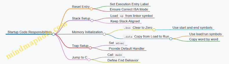
Example: Minimal Assembly Startup for RISC-V
This example assumes the linker provides symbols for stack and memory boundaries. The exact symbol names depend on your linker script, but the pattern is consistent.
    .section .text
    .globl _start
_start:
    la   sp, _stack_top

    # Clear .bss
    la   t0, __bss_start
    la   t1, __bss_end
    li   t2, 0
1:
    bge  t0, t1, 2f
    sw   t2, 0(t0)
    addi t0, t0, 4
    j    1b
2:
    # Copy .data from Load to Run
    la   t0, __data_start
    la   t1, __data_end
    la   t3, __data_load
3:
    bge  t0, t1, 4f
    lw   t4, 0(t3)
    sw   t4, 0(t0)
    addi t0, t0, 4
    addi t3, t3, 4
    j    3b
4:
    call main
hang:
    j hang
A few practical notes:
- Use word operations (
lw/sw) when your memory is word-aligned and your ABI expects 32-bit accesses. If you target RV64, adjust told/sdand step by 8. - If your
.datasize isn’t a multiple of the access width, you need a byte-wise copy loop or ensure alignment in the linker script.
Example: Trap Setup That Doesn’t Break Bring-Up
Even a minimal handler prevents “mystery resets” when something goes wrong early. A common approach is to set mtvec to a handler that loops.
    .section .text
    .globl default_trap
default_trap:
    j default_trap

    .section .text
    .globl _start
_start:
    la   sp, _stack_top
    la   t0, default_trap
    csrw mtvec, t0
    # Then Continue with Bss/data Init and Call Main
Systematic Debug Checklist for Memory Initialization
When bring-up fails, check these in order:
- Stack pointer sanity: confirm
_stack_toppoints into valid RAM and is aligned. - BSS boundaries: verify
__bss_start <= __bss_endand that the region is writable. - Data load vs run: confirm
__data_loadis reachable at reset (for example, mapped ROM or flash region) and that__data_startis in RAM. - Bus width and alignment: if your LiteX bus or RAM model expects aligned accesses, unaligned copies can stall or fault.
- mtvec correctness: if traps occur during initialization, a wrong
mtveccan cause repeated faults.
Putting It Together with a Linker Contract
Startup code is only as good as the symbols it relies on. Treat the linker script as a contract: it defines boundaries for .bss, .data, and the stack. Your assembly should never “guess” sizes or addresses. When the contract is consistent, the rest of the system—C code, peripherals, and simulation—becomes much easier to reason about.
7.3 Implementing UART or GPIO Based Diagnostics
Diagnostics are the fastest way to turn “it doesn’t work” into “it fails at this exact moment.” In a LiteX-based RISC-V SoC, you typically want two things: a low-effort way to print state (UART) and a low-latency way to signal events (GPIO). The key is to design both so they are usable during early bring-up, before software drivers are fully trustworthy.
Foundational Principles for Reliable Diagnostics
Start with a simple contract between hardware and software:
- Deterministic triggers: each diagnostic output should correspond to a specific event, not a vague “something happened.”
- Bounded overhead: diagnostics must not stall the CPU indefinitely. If UART is slow, avoid blocking writes.
- Clear encoding: choose a consistent format for messages or GPIO patterns so you can interpret them quickly.
- Reset behavior: define what the UART TX and GPIO pins do immediately after reset.
A practical approach is to implement a small hardware “diagnostic event” module that receives event codes from the SoC and then routes them to UART and/or GPIO.
UART Diagnostics That Don’t Get in the Way
UART is ideal for human-readable logs, but it needs careful handling to avoid turning a timing problem into a software problem.
Minimal UART transmit strategy
- Use a UART TX peripheral with a transmit FIFO or a simple ready/valid handshake.
- In your diagnostic path, convert event codes into a short message like
EVT 0x12plus a newline. - If the UART is busy, either drop the message or keep only the latest one. Dropping is often better than deadlocking.
Example event encoding
- Define event IDs for common bring-up milestones: boot start, first instruction fetch, trap entry, bus error, and peripheral init.
- Keep the mapping in software as constants so the same IDs are used in both hardware and tests.
UART message format
- Keep messages short and fixed-width where possible.
- Include a small checksum-like pattern only if you already have it; otherwise, rely on consistent formatting.
GPIO Diagnostics for Cycle-Accurate Clues
GPIO is useful when UART output is too slow or when you need to observe behavior with a logic analyzer.
GPIO design choices
- Use a small set of pins as an event code bus, for example 4 or 8 bits.
- Latch the event code on the rising edge of an event strobe.
- Optionally add a “valid” pin so you can distinguish idle from active.
Example GPIO pattern
GPIO[7:0]holds the event ID.GPIO_VALIDgoes high for one or more cycles after an event.- Software can also read back event registers if you expose them, but the primary goal is external visibility.
Mind Map: UART and GPIO Diagnostics
Systematic Implementation Flow
- Define event IDs: pick a small set first. For example,
EVT_BOOT_START=0x01,EVT_TRAP=0x10,EVT_BUS_ERROR=0x20. - Add a diagnostic event interface: a hardware module receives
event_idandevent_strobe. - Route to UART: format
event_idinto a short string and attempt transmit without stalling. - Route to GPIO: latch
event_idon strobe and assertGPIO_VALID. - Connect to real triggers: wire event strobes to points you can reason about, such as trap entry and bus error handling.
- Write minimal software: print a single “boot start” message and then rely on hardware events for the rest.
- Validate with targeted tests: in simulation, force the same triggers and confirm the emitted UART text and GPIO codes match.
Example: Event Triggering and Routing
Below is a conceptual hardware-side sketch showing the separation between event capture and output routing. It is intentionally small so you can map it to your existing LiteX/SoC structure.
// Conceptual diagnostic event router
module diag_router(
  input  wire        clk,
  input  wire        rst,
  input  wire [7:0] event_id,
  input  wire        event_strobe,
  output reg  [7:0] gpio_code,
  output reg         gpio_valid,
  output wire        uart_tx_valid,
  output wire [7:0] uart_tx_payload
);
  always @(posedge clk) begin
    if (rst) begin
      gpio_code  <= 8'h00;
      gpio_valid <= 1'b0;
    end else begin
      gpio_valid <= 1'b0;
      if (event_strobe) begin
        gpio_code  <= event_id;
        gpio_valid <= 1'b1;
      end
    end
  end

  // UART payload is the raw event_id; formatter lives elsewhere
  assign uart_tx_payload = event_id;
  assign uart_tx_valid   = event_strobe;
endmodule
This split keeps GPIO timing straightforward and makes UART formatting a separate concern. In practice, your UART formatter can translate uart_tx_payload into a fixed message only when uart_tx_valid is asserted.
Practical Bring-Up Example
A common failure mode is “CPU never reaches software.” In that case:
- Assert
EVT_BOOT_STARTright after reset release. - Assert
EVT_TRAPon trap entry. - Assert
EVT_BUS_ERRORwhen the bus interface reports an error.
If you see EVT_BOOT_START on GPIO but never see EVT_TRAP, you likely have a reset/clock issue or the CPU is stuck before trap handling. If you see EVT_TRAP but no UART text, the UART path is miswired or the transmit logic is blocked. Either way, you get a concrete next step instead of guessing.
The most important habit is to make each diagnostic event correspond to a single, well-defined hardware condition. When that discipline is in place, UART and GPIO stop being “extra signals” and become a reliable timeline of what the SoC is doing.
7.4 Exercising CSR and Exception Paths With Targeted Tests
A bring-up test that only checks “it boots” is like checking a car starts without ever pressing the brakes. CSR and exception paths are where correctness shows up under stress: illegal instructions, misaligned accesses, page faults, and the exact values written to CSRs during traps.
Foundations: What You Must Observe
Start by listing the observable outcomes your tests can check:
- The trap cause value (often in
mcauseorscausedepending on privilege mode). - The trap program counter (often
mepcorsepc). - The privilege mode transition behavior (e.g.,
mstatusfields). - The interrupt enable state after trap entry and after
mret. - Whether the faulting instruction is retried or skipped (based on how
mepcis set).
A practical rule: every test should have a single “fault trigger” and a single “expected CSR snapshot.” If you mix multiple triggers, you’ll spend more time untangling than validating.
Mind Map: CSR and Exception Test Strategy
Building a Deterministic Trap Harness
Use a trap handler that writes CSR values to a known memory region or prints them via UART. Determinism matters: if your handler depends on timing or uninitialized memory, you’ll get “sometimes correct” results.
A simple harness pattern:
- Install trap vector (in machine mode, set
mtvecto a handler address). - Enable the specific interrupt source only when testing interrupts.
- Execute a short instruction sequence that triggers exactly one exception.
- In the handler, read CSRs and record them.
- Return with
mretand confirm control flow.
Example: Illegal Instruction Trap with CSR Snapshot
Goal: confirm mcause reports an illegal instruction and mepc points to the faulting instruction.
Test steps:
- Place an illegal instruction at a known label.
- Execute it.
- In the trap handler, read
mcauseandmepc. - After
mret, write a “passed” marker.
Key checks:
mcauseequals the illegal-instruction exception code.mepcequals the address of the illegal instruction label.- The handler does not corrupt the stack pointer or the return address.
Example: Misaligned Access Trap with Address Reasoning
Misaligned loads/stores are great because the expected behavior is precise and easy to reason about.
Test steps:
- Choose a base address aligned to a word boundary.
- Perform a load from
base + 1using a word load instruction. - In the handler, record
mcauseandmepc.
Key checks:
mcausematches the misaligned access exception.mepcpoints to the misaligned load instruction.- If your platform supports it, verify whether the faulting instruction is retried or skipped by observing whether the “passed” marker is reached only once.
Example: Environment Call Trap and Return Semantics
An ecall is useful because it’s intentional and repeatable.
Test steps:
- Execute
ecallfrom a known instruction address. - In the handler, record
mcauseandmepc. - Return with
mret.
Key checks:
mcausematches the environment-call cause for the current privilege level.mepcpoints to theecallinstruction.- After
mret, execution continues at the correct next instruction. If your implementation incrementsmepcin the handler, verify that behavior explicitly by comparing the observed next PC to the expected one.
Advanced Details: What Breaks in Real Designs
- CSR read timing: If your RTL updates CSR registers in the wrong cycle relative to trap entry, simulation might still “look fine” until you check exact values.
mepcselection: Some bugs setmepcto the next PC instead of the faulting PC. Your tests should compare against the label address, not just “some PC.”- Interrupt enable bits: After trap entry, the interrupt enable state should match the spec behavior your core implements. Record
mstatusfields and validate them, not justmcause. - Handler reentrancy: If your handler triggers another trap (for example, by touching an unmapped address), you’ll see nested behavior. Keep the handler’s memory accesses minimal and safe.
Validation Loop: Tighten One Expectation at a Time
Run the test in simulation first, then on FPGA. When a mismatch occurs, change only one variable per iteration:
- If
mcauseis wrong, focus on exception decode. - If
mepcis wrong, focus on PC selection and pipeline timing. - If
mstatusbits are wrong, focus on trap entry/exit sequencing.
A good final check is a “matrix” of tests: illegal instruction, misaligned access, and ecall, each with a CSR snapshot and a control-flow marker after mret. When all three pass with exact CSR values, you’ve validated both the trap mechanism and the correctness of the state you rely on during bring-up.
7.5 Integrating Software Tests with Hardware Test Expectations
Software tests are only useful if they know what the hardware is supposed to do. Integration means aligning three things: the software’s observable behavior, the hardware’s timing and side effects, and the test harness’s pass fail criteria. The goal is not to “test everything,” but to make each test answer a specific question with evidence.
Start with a shared contract. For each peripheral and system service, define a small set of expectations: which registers change, which interrupts fire, what UART output looks like, and what happens on error paths. Then map those expectations to software assertions. For example, if a UART TX register is memory-mapped, the software test should confirm that writing a byte eventually results in that byte appearing on the UART receive side (loopback or external capture), not merely that the write completed.
Next, decide what “time” means in your tests. Hardware often has latency: bus transactions take cycles, FIFOs buffer data, and interrupts may be delayed until a condition is stable. In simulation, you can use cycle-accurate stepping. On FPGA, you may need wall-clock timeouts. Keep the same logical structure in both environments: wait for an event, bound the wait, then check the observed result. A test that waits forever is a test that teaches you nothing.
Then integrate the test harness with the SoC’s debug visibility. If your design exposes a UART console, a memory-mapped trace buffer, or a set of status registers, the software test can read those values and report structured results. The hardware side can also provide “breadcrumbs,” such as a register that increments on each completed bus transaction or on each interrupt entry. This makes failures actionable: you can tell whether the CPU ran, whether the peripheral saw the request, and whether the expected completion signal occurred.
A practical pattern is the three-phase test: setup, stimulus, and verification.
- Setup: initialize memory map regions, configure peripheral registers, and clear any sticky status bits.
- Stimulus: perform the software action under test, such as writing a control register, sending bytes over UART, or triggering a timer.
- Verification: confirm both software-level state and hardware-level evidence, such as reading back status registers and checking that an interrupt was observed.
Below is a concrete example for a memory-mapped timer that generates an interrupt.
Example: Timer interrupt test with bounded waiting
- Software clears the timer interrupt pending bit.
- Software programs the compare value and enables the interrupt.
- Software starts the timer.
- Software waits until an interrupt flag is observed, using a bounded loop.
- Software reads a “last match” register and verifies it equals the programmed compare value.
- Software acknowledges the interrupt and confirms the pending bit clears.
If any step fails, the software prints a structured line like TIMER_FAIL step=wait_pending pending=1 last_match=0x... so the hardware logs can be correlated.
Mind Map: Software Tests Aligned with Hardware Expectations
Example: Step-Tagged Assertions for Faster Triage
When a test fails, you want to know which contract clause broke. Use step tags that correspond to the hardware expectation.
step=setup_clear_pending pending_before=1 pending_after=0
step=program_compare compare=0x00000100
step=start_timer running=1
step=wait_interrupt pending=1 cycles=12345
step=verify_last_match last_match=0x00000100
step=ack_interrupt pending_after_ack=0
This format lets you compare simulation and FPGA runs without guessing. If wait_interrupt times out, the issue is likely interrupt generation or enable wiring. If pending becomes 1 but last_match is wrong, the peripheral logic is suspect even if the interrupt path works.
Finally, keep the software tests deterministic. Avoid relying on unspecified ordering between independent events. If your design has multiple interrupts or concurrent DMA-like transfers, structure tests so only one stimulus is active at a time, or so the verification checks a known sequence. Determinism makes your pass fail criteria meaningful rather than hopeful.
A good integration ends with a single rule: every software test must name the hardware evidence it expects, and every hardware evidence must be reachable and checkable from the software test harness.
8. FPGA Implementation and Timing Closure for Open Designs
8.1 Preparing Synthesis and Constraints for Target FPGA Devices
Synthesis and constraints are where “it works in simulation” turns into “it works on silicon.” The goal is to make the FPGA tools understand three things precisely: the clocking intent, the timing requirements, and the physical reality of pins and IO standards. If any of those are vague, the tools will guess, and guesses are rarely friendly.
Foundational Inputs You Must Lock Down
Start by freezing the target device and board-level assumptions. Confirm the exact FPGA part number, package, speed grade, and the board’s clock sources. Then list the top-level ports that must be constrained: clocks, resets, UART/JTAG pins, and any external buses.
Next, decide what “timing closure” means for your design. For a simple SoC, you typically care about the CPU clock domain and any peripheral domains. If you have multiple clocks, you must state which paths are allowed to cross domains and how they are synchronized.
Finally, ensure your RTL is tool-friendly. Use explicit clock and reset signals at module boundaries, avoid inferred latches, and keep asynchronous resets clearly marked. A constraint file cannot fix a reset that is effectively random from the tools’ perspective.
Clock Constraints That Match Reality
Clock constraints are the backbone of timing analysis. Define each clock with its period and waveform. If the board uses a PLL or MMCM, constrain the generated clock too, using the actual output frequency and phase relationship when known.
For example, suppose your design uses a 50 MHz input clock and generates a 100 MHz internal clock. You constrain the input clock at 20 ns period, then constrain the 100 MHz generated clock at 10 ns. If you skip the generated clock, the tools may analyze timing against the wrong reference.
Also specify clock domain crossings. If you use synchronizers, the timing requirement across the synchronizer is usually less strict than the requirement within the source and destination domains. The tools need to know where the boundaries are.
IO Constraints and Electrical Correctness
Pin constraints map logical ports to physical pins. Along with pin locations, you must set IO standards, drive strength, slew rate, and termination if required by the board. A mismatch here can cause failures that look like “timing problems” but are actually electrical.
A practical approach is to treat IO constraints as part of the design contract. For each external interface, record: the port names, expected voltage standard, and any special requirements like differential pairs.
Reset and Multicycle Path Discipline
Resets deserve special attention. If your reset is asynchronous, constrain it as such and ensure it is not treated as a normal synchronous signal. If your reset is synchronous, make sure it is released only on the active clock edge.
For timing exceptions, use them sparingly and intentionally. A common case is a register-to-register path that is allowed extra cycles due to pipeline stages. Use multicycle constraints only when the RTL structure guarantees the extra time. If you apply multicycle constraints to a path that sometimes needs the full cycle, you’ll get a “closed” timing report that still fails in hardware.
A Systematic Constraint Workflow
- Start with a minimal constraint set: clocks, resets, and IO pin mapping.
- Run synthesis and initial place and route to surface missing constraints.
- Iterate on timing: add false paths, multicycle paths, and clock groupings only after you see the tool’s warnings.
- Re-check after RTL changes: even small changes can alter critical paths.
Mind the difference between “no warnings” and “correct constraints.” The first is a hygiene check; the second is correctness.
Mind Map: Synthesis and Constraints Checklist
Example: Two Clock Domains with a UART
Assume your design has:
clk_cpuat 100 MHzclk_ioat 25 MHz- UART logic in the
clk_iodomain
You constrain both clocks. Then you group them as asynchronous if there is no defined phase relationship. For the UART, you constrain its internal timing within clk_io. If you transfer UART status into the CPU domain, you use a synchronizer and constrain the CPU domain timing separately.
If you instead treat the two clocks as related, the tools may try to meet timing on paths that should not be directly timed, leading to either overly strict constraints or misleading closure.
Example: Multicycle Path for a Pipelined Peripheral Register
Suppose a peripheral register write goes through a two-stage pipeline before it affects a control signal. If the RTL guarantees that the control signal only changes after two cycles, you can apply a multicycle constraint from the pipeline input register to the output register.
The key is matching the constraint to the RTL structure. If the pipeline depth changes due to synthesis optimizations, the constraint must still reflect the actual register-to-register behavior.
Practical Output Artifacts to Capture
When you run synthesis and implementation, capture:
- The constraint file used
- The generated clock list and their periods
- The timing summary and top critical paths
- Any warnings about unconstrained ports or clocks
Treat these as part of the build record. When a later change breaks timing, you want to compare constraint intent, not just waveforms.
By the time you reach place and route, your constraints should read like a precise description of the hardware’s timing and electrical contract. The tools can then do their job without guessing.
8.2 Managing Clock Domains and Reset Synchronization
A clock domain is a region of logic that shares the same clock signal. Reset synchronization is the art of making sure every flip-flop sees reset deassertion at a safe time relative to its clock. If you skip this, you may get “works on my board” behavior where some registers start in the wrong state and only fail under certain timing.
Foundational Concepts for Safe Reset
Start by separating two ideas: synchronous reset and asynchronous reset.
- Synchronous reset means reset is sampled by the clock. Deassertion is naturally aligned to the clock edge, so you often avoid extra synchronizers.
- Asynchronous reset means reset can change without waiting for a clock edge. This is convenient for bringing up hardware, but deassertion must be synchronized to each clock domain.
Even when you use asynchronous reset, you typically want synchronous deassertion. The usual pattern is: assert reset asynchronously, then release it through a small synchronizer chain per clock domain.
Clock Domain Boundaries and What Crosses Them
A clock domain boundary is where signals move between different clocks. You must decide what kind of crossing you have:
- Single-bit control signals crossing domains: use a two-flop synchronizer.
- Multi-bit buses crossing domains: use a handshake, a FIFO, or a bus synchronizer strategy that guarantees atomicity.
- Reset crossing: treat reset deassertion as a control signal that must be synchronized per destination clock.
A practical rule: if a signal is sampled by flip-flops in a different clock domain than where it is generated, assume you need a crossing strategy.
Reset Synchronization Strategy per Clock Domain
For each clock domain, create a reset synchronizer module that produces a clean local reset.
Core behavior:
- Keep local reset asserted while the source reset is asserted.
- When the source reset deasserts, wait for a few local clock edges before releasing local reset.
- Use at least two flip-flops for deassertion synchronization.
This prevents metastability from propagating into the logic that depends on reset being stable.
Example: Two-Flip-Flop Reset Deassertion
module reset_sync(
  input  wire clk,
  input  wire rst_n_async,
  output wire rst_n_sync
);
  reg [1:0] ff;
  always @(posedge clk or negedge rst_n_async) begin
    if (!rst_n_async) ff <= 2'b00;
    else ff <= {ff[0], 1'b1};
  end
  assign rst_n_sync = ff[1];
endmodule
In this pattern, the asynchronous reset assertion is immediate, but deassertion becomes aligned to the destination clock after two cycles.
Handling Multiple Resets and Reset Trees
In FPGA designs, you often have a global reset source feeding multiple domains. A reset tree should be deterministic:
- Ensure each domain has its own synchronizer instance.
- Avoid mixing synchronized and unsynchronized reset signals in the same domain.
- Keep reset polarity consistent across modules to reduce wiring mistakes.
If you have a “system reset” and a “peripheral reset,” treat them as separate control paths. Synchronize each one to the clock domain that consumes it.
Reset Release Ordering and Dependency Management
Some blocks depend on others being ready. For example, a UART transmitter might depend on a baud-rate generator being stable. Reset ordering can be handled without global sequencing by using local “ready” gating.
A common approach:
- Synchronize reset deassertion.
- Add a small counter or shift register that waits a fixed number of cycles before enabling dependent logic.
This is not about guessing timing; it’s about making the enable condition explicit and repeatable.
Example: Enable After N Cycles
module delayed_enable(
  input  wire clk,
  input  wire rst_n,
  input  wire start,
  output wire en
);
  reg [3:0] cnt;
  always @(posedge clk) begin
    if (!rst_n) cnt <= 0;
    else if (start && cnt != 4'd10) cnt <= cnt + 1;
  end
  assign en = (cnt == 4'd10);
endmodule
Here, dependent logic can use en rather than assuming reset release alone guarantees readiness.
Mind Map: Clock Domains and Reset Synchronization
Verification Checklist That Actually Catches Bugs
- Confirm every clock domain has a reset synchronizer for deassertion.
- Search for any direct use of an asynchronous reset signal inside sequential logic without synchronization.
- In simulation, add assertions that check reset deassertion behavior: local reset must remain asserted for at least two destination clock edges after the source deasserts.
- For bus crossings, ensure reset does not create partial updates across domains.
When these checks pass, you’ve removed a whole class of timing-dependent startup failures—usually the kind that show up only after the bitstream is already loaded and you’re trying to look calm.
8.3 Handling IO Standards and Pin Assignments for Debug Interfaces
Debug interfaces are where “it should work” meets “it actually works.” On FPGA boards, the most common bring-up failures come from mismatched IO standards, incorrect pin direction, and resets that leave the debug logic half-alive. This section treats debug IO as a disciplined hardware interface: define electrical requirements, map them to FPGA constraints, and validate the result with a short, deterministic checklist.
Foundational Electrical Requirements
Start by listing every debug signal and its electrical role:
- JTAG: TCK, TMS, TDI, TDO, and often TRST and SRST. These pins must match the board’s JTAG voltage domain.
- UART: TXD and RXD. UART is usually single-ended and sensitive to voltage levels and pull-ups.
- GPIO debug: LEDs, test points, and “scope-friendly” toggles. These often need correct drive strength and pull configuration.
For each signal, record:
- Voltage domain (e.g., 3.3 V bank vs 1.8 V bank)
- Direction (FPGA drives vs FPGA receives)
- Termination and bias (pull-up, pull-down, or none)
- Speed expectations (JTAG is fast enough to punish sloppy constraints; UART is forgiving but not immune)
A practical rule: if the board manual says the debug header is in a specific IO bank voltage, your FPGA constraints must follow that bank voltage exactly. “Close enough” is not a strategy for IO standards.
IO Standards and Bank Selection
In FPGA constraints, IO standards typically appear as a per-pin or per-bank setting. The key idea is that IO standard is electrical behavior, not just metadata. If you set an IO standard that doesn’t match the board’s voltage, you can get symptoms like:
- JTAG reads as stuck
- UART characters look like random noise
- GPIO levels never cross the receiver threshold
When you assign pins, do it in two passes:
- Assign pins to packages (physical location)
- Assign IO standards to those pins (electrical behavior)
Keep the passes separate so you can spot mismatches quickly.
Pin Assignment Workflow for Debug Headers
Use a repeatable workflow that mirrors how constraints are applied in synthesis and implementation:
- Create a dedicated constraints section for debug IO so it’s easy to audit.
- Group pins by interface (JTAG group, UART group, GPIO group).
- Set pull-ups/pull-downs explicitly for any signal that can float during reset.
- Confirm clock-related pins for JTAG are not accidentally routed through logic that changes their timing.
A small but effective habit: add a “known-good” LED or GPIO that toggles from a reset-safe clock domain. If that pin is wrong, you’ll know immediately that the IO bank or pin mapping is wrong.
Example Mind Map
Mind Map: Debug IO Standards and Pin Assignments
Concrete Constraint Example
Below is a compact example showing the intent: pin mapping plus IO standard plus bias. Adjust names to match your project.
# Debug UART pins
set_property PACKAGE_PIN P12 [get_ports {uart_rx}]
set_property IOSTANDARD LVCMOS33 [get_ports {uart_rx}]
set_property PULLUP true [get_ports {uart_rx}]

set_property PACKAGE_PIN P13 [get_ports {uart_tx}]
set_property IOSTANDARD LVCMOS33 [get_ports {uart_tx}]

# JTAG Pins
set_property PACKAGE_PIN K1 [get_ports {tck}]
set_property IOSTANDARD LVCMOS33 [get_ports {tck}]

set_property PACKAGE_PIN L1 [get_ports {tdi}]
set_property IOSTANDARD LVCMOS33 [get_ports {tdi}]

set_property PACKAGE_PIN M1 [get_ports {tdo}]
set_property IOSTANDARD LVCMOS33 [get_ports {tdo}]
If your board uses 1.8 V for JTAG, the IO standard must change accordingly. The pin numbers alone don’t guarantee correct electrical behavior.
Validation Checklist That Catches Real Problems
Once constraints are in place, validate in this order:
- JTAG link: confirm the debugger can see the device. If it can’t, suspect IO standard, pin mapping, or reset behavior.
- UART sanity: send a known pattern from the FPGA and verify it on the host. If characters are garbled, check voltage levels and RX pull configuration.
- Reset-safe GPIO: confirm a test pin toggles immediately after configuration. If it doesn’t, the pin mapping or IO bank is wrong, not the logic.
This order reduces wasted time because each step narrows the fault domain from “electrical connectivity” to “protocol correctness.”
Common Failure Modes and How to Fix Them
- Wrong IO standard: symptoms are consistent across interfaces in the same bank. Fix by matching the board’s header voltage domain in constraints.
- Floating RX pins: UART RX can randomly frame during reset. Fix by adding an explicit pull-up or pull-down matching the expected idle level.
- Direction mismatch: swapping TX/RX in ports compiles fine but produces silence or nonsense. Fix by aligning port naming with physical direction and re-checking the constraints.
- Reset interaction: debug logic may be held in reset longer than expected. Fix by ensuring reset synchronizers and debug enable signals are defined for the debug clock domain.
Treat debug IO as a first-class interface: precise electrical constraints, explicit biasing, and a short validation sequence. That’s how you turn “debugging the debugger” into a predictable routine.
8.4 Interpreting Timing Reports and Fixing Common Violations
Timing reports look like a wall of numbers until you learn what each number is trying to tell you. The goal is simple: identify the violating path, understand why it violates, then apply the smallest change that fixes it without breaking functionality.
Start with the Report Summary
Begin by locating the worst negative slack (WNS) and total negative slack (TNS). WNS tells you the single most critical failure; TNS tells you how much total “timing debt” exists across all failing paths. If WNS is slightly negative but TNS is large, you may have many marginal paths rather than one catastrophic one.
Next, confirm the report is for the correct clock domain and the correct analysis mode. A common mistake is reviewing a report generated for a different constraint set than the one used in the build, or reading a path group that doesn’t match your real register-to-register intent.
Identify the Failing Path Type
Most violations fall into a few buckets:
- Setup violations: data arrives too late before the capturing clock edge.
- Hold violations: data arrives too early after the launching edge.
- Multicycle or false path issues: constraints don’t match the design’s actual behavior.
- Clocking and reset path issues: asynchronous resets or poorly synchronized signals create unexpected timing paths.
A quick sanity check: if you see both setup and hold problems on the same path group, you likely have a constraint mismatch or a clock/reset handling issue rather than a single slow combinational block.
Read the Path Breakdown Like a Story
For a setup path, the report usually provides a breakdown such as launch clock edge, data path delay, capture clock edge, and required time. The slack is essentially:
- Slack = Required Time − Arrival Time
So when you see negative slack, focus on which component is pushing arrival time later. If the report lists large logic delay, you need to reduce combinational depth or improve placement. If the report lists large routing delay, you may need floorplanning, buffering, or a different synthesis strategy.
For hold paths, the story flips: the required time is very close to the launch edge, so small routing changes can break hold even if setup looks fine. If hold is failing, don’t immediately “speed up” logic; instead, check whether the path should be constrained as multicycle or whether the design uses proper synchronization.
Mind Map: a Systematic Fix Strategy
Timing Fix Workflow Mind Map
Common Violations and Practical Fixes
Setup Violation on a Register-to-Register Path
If the failing path is a long combinational chain between two registers, the most reliable fix is pipelining. Add a register boundary at a natural stage boundary, such as after instruction decode or before a wide peripheral register decode. Then re-run timing and verify that the new pipeline stage doesn’t change the architectural latency expected by software.
If you can’t add a pipeline stage, reduce logic depth. For example, replace a wide priority mux with a smaller staged selection, or ensure that decode signals are one-hot where appropriate so the synthesis tool can simplify logic.
Hold Violation After a Pipeline Change
Hold problems often appear after you fix setup by adding registers. The new pipeline can reduce the minimum delay on some paths. A typical fix is to add a small amount of delay on the affected path, such as inserting a buffer or using a controlled register retiming strategy. If the report indicates the path is through a synchronizer, double-check that the synchronizer is implemented as a proper two-flop chain and that you are not accidentally timing an asynchronous signal directly into the logic.
Constraint Mismatch That Looks Like “Bad Hardware”
When constraints are wrong, the timing report can blame the design unfairly. Verify that:
- The clock period matches the actual FPGA clock you will use.
- Generated clocks have correct source and division factors.
- Input/output delays are consistent with your IO timing model.
- Multicycle constraints match the real behavior of the path group.
A classic example: a bus interface that intentionally allows one extra cycle for a handshake may be constrained as single-cycle, causing setup violations that disappear once multicycle is applied correctly.
Reset and Clocking Violations
Reset-related timing can be tricky because asynchronous reset deassertion can create paths that don’t exist in a purely synchronous model. If the report shows reset release paths with negative slack, ensure your reset strategy is consistent: use a reset synchronizer where required, and confirm that the synthesis and implementation tools are treating reset signals as intended.
A Concrete Example Workflow
Suppose the report shows WNS = −0.12 ns on a setup path in the CPU control logic. The breakdown shows routing delay dominates, and the path crosses a region boundary. First, check the path group name to confirm it’s truly the CPU clock domain. Then inspect the netlist hierarchy for high fanout control signals feeding the failing logic. If the signal fans out broadly, register it closer to the consumer or reduce fanout by restructuring the logic so fewer gates depend on the same control net.
After the RTL change, re-run timing and confirm that hold is not worse. If hold becomes negative, you likely reduced minimum delay too much; add a small pipeline register stage or apply a targeted delay fix to the specific path group rather than changing the entire design.
Verification Checklist Before You Declare Victory
- WNS is non-negative for the intended clock domain.
- TNS is reduced to an acceptable level for your risk tolerance.
- Hold violations are checked after every setup fix.
- The constraint set used for the report matches the build configuration.
- Functional behavior is preserved, especially for pipeline latency and handshake timing.
Timing closure is less about heroics and more about disciplined iteration: interpret, classify, fix the smallest plausible cause, then validate with both setup and hold in mind.
8.5 Producing Bitstreams and Capturing Build Metadata
A bitstream is the end product of a chain of deterministic steps: synthesis, placement, routing, and finally configuration file generation. Capturing build metadata turns that chain into something you can audit, reproduce, and compare when hardware behavior changes.
Foundational Inputs That Must Be Logged
Start by listing the inputs that affect the output bitstream. At minimum, capture:
- Target FPGA part number and package.
- Tool versions for synthesis, place and route, and bitstream generation.
- Constraint sources, including pin constraints and timing constraints.
- Top-level HDL commit hash and any generated Verilog sources.
- Build parameters such as SoC configuration, memory map base addresses, and clock frequencies.
A practical rule: if you can’t explain why two bitstreams differ, you didn’t log enough.
Bitstream Production Workflow with Checkpoints
Treat the build as a pipeline with checkpoints. Each checkpoint should produce both artifacts and a small summary file.
- Synthesis checkpoint
- Output: synthesized netlist or intermediate representation.
- Summary: resource estimates and warnings.
- Implementation checkpoint
- Output: placed and routed design database.
- Summary: timing report highlights, especially worst negative slack and critical path description.
- Bitstream checkpoint
- Output: .bit or .bin file plus any vendor-specific headers.
- Summary: bitstream generation log and final status.
A simple sanity check is to compute a hash of the final bitstream and store it alongside the metadata. If the hash changes, you have a concrete reason to investigate.
Metadata Schema That Stays Useful
Use a metadata file that is easy to diff. A good schema includes:
- Build identity: build ID, timestamp, and git commit.
- Environment: tool versions and host OS details.
- Inputs: constraints file names and checksums, HDL source checksums, and parameter values.
- Outputs: bitstream file name, size, and hash.
- Evidence: paths to timing reports and implementation summaries.
If you include checksums for constraint files and generated HDL, you can detect “same commit, different build inputs” situations.
Mind Map: Bitstream Outputs and Metadata
Example: Capturing a Minimal Metadata File
Below is a compact metadata template you can generate during the build. It’s intentionally plain so it survives across toolchains.
{
  "build_id": "2025-03-12_1530",
  "date": "2025-03-12",
  "git": {"commit": "<hash>", "dirty": false},
  "fpga": {"part": "<vendor_part>", "package": "<pkg>"},
  "tools": {
    "synth": "<version>",
    "place_route": "<version>",
    "bitgen": "<version>"
  },
  "params": {"clk_hz": 50000000, "mem_base": "0x80000000"},
  "inputs": {
    "constraints_sha256": "<sha>",
    "hdl_sha256": "<sha>"
  },
  "outputs": {
    "bitstream_file": "build/top.bit",
    "bitstream_sha256": "<sha>",
    "bitstream_size_bytes": 1234567
  },
  "evidence": {
    "timing_report": "build/reports/timing.rpt",
    "util_report": "build/reports/util.rpt"
  }
}
Example: Hashing and Comparing Bitstreams
When you suspect a hardware mismatch, compare metadata first, then bitstream hashes. A bitstream hash mismatch is a strong signal that the design changed even if the software image stayed the same.
# Compute Hashes for Evidence
sha256sum build/top.bit > build/bitstream.sha256
cat build/bitstream.sha256

# Compare Against a Previous Build
sha256sum -c build/bitstream.sha256.prev
Advanced Details That Prevent Pain Later
- Log the exact constraint file set. Many flows silently include defaults; record what was actually used.
- Capture timing report excerpts, not just the file path. The worst slack number and the critical path endpoints are the parts you’ll want during triage.
- Record clocking assumptions. If your design uses multiple clock domains, log the constraints that define each domain’s frequency and relationships.
- Store the implementation database when feasible. It can save time when you need to understand why routing changed.
Validation Checklist Before You Call It Done
Before moving on to hardware validation, confirm:
- The bitstream exists and its hash is recorded.
- Metadata references the correct timing and utilization reports.
- Parameter values match the software build assumptions.
- The build ID is unique and traceable to the git commit.
A build that produces a bitstream without metadata is like a lab notebook with the pages torn out. The FPGA will still work, but you’ll have to guess why.
9. FPGA Validation Pipelines from Bitstream to Measured Results
9.1 Defining Validation Objectives and Pass Fail Criteria
Validation objectives answer one question: what must be true for the hardware to be considered correct for the intended use. Pass fail criteria answer a second question: how you will measure “true” in a way that is repeatable, automatable, and specific enough to catch regressions.
Start with a Single Validation Story
Pick one end-to-end story that matches your bring-up stage. For example: “A minimal RISC-V program boots from ROM, writes a known pattern to a memory-mapped UART TX register, and the host observes the expected characters.” This story forces you to define boundaries: what counts as success, what counts as failure, and what you will not test yet.
A practical objective set usually includes three layers:
- Functional correctness: the SoC behaves according to the spec you wrote for it.
- Interface correctness: bus transactions, interrupts, and register semantics match expectations.
- Integration correctness: the CPU, memory map, peripherals, and boot flow agree on addresses, widths, and timing assumptions.
Translate Objectives into Measurable Claims
Turn each objective into a claim that can be checked. A claim has inputs, an expected observation, and a tolerance.
Example claims for a UART-based bring-up:
- Boot claim: after reset deassertion, the program reaches the UART write loop within N cycles.
- Register claim: writing value 0x41 to UART TX results in exactly one transmitted byte with ASCII ‘A’.
- No spurious writes claim: during a defined idle window, no additional UART bytes appear.
Each claim should specify:
- Where you observe it (UART log, memory probe, CSR readback, bus monitor).
- What you compare (byte values, sequence order, counts).
- What tolerance means (cycle window, allowed retries, reset latency).
Define Pass Fail Criteria with Explicit Thresholds
Pass fail criteria should be strict where correctness matters and forgiving where physical timing varies.
Use a small set of criterion types:
- Exact match: expected bytes, expected register values, expected exception codes.
- Range match: timing windows like “interrupt asserted within 50–200 cycles.”
- Invariants: properties that must always hold, such as “no bus read occurs from unmapped addresses.”
- Absence criteria: “no X or Z on critical signals” in simulation, or “no UART framing errors” in hardware.
Concrete example thresholds:
- Boot success: UART prints “BOOT_OK\n” within 10,000 cycles.
- UART correctness: transmitted bytes equal the expected string exactly; any mismatch fails.
- Stability: run the same test for 100 iterations; any intermittent failure fails.
Build a Criteria Matrix That Maps Tests to Claims
A matrix prevents the common failure mode where tests exist but no one can explain what they prove.
| Test | Objective Claim | Observation Source | Pass Criteria | Fail Criteria |
|---|---|---|---|---|
| Boot Smoke | CPU reaches boot loop | UART log | “BOOT_OK” appears once | Missing or wrong string |
| UART TX Pattern | TX register semantics | UART bytes | Exact byte sequence | Wrong order, extra bytes |
| CSR Readback | CSR access correctness | Verilator trace or debug reads | Expected CSR values | Unexpected values or traps |
| Bus Safety | No unmapped accesses | Bus monitor | Zero unmapped transactions | Any unmapped read/write |
Mind Map: Validation Objectives and Pass Fail Criteria
Example: A Complete Objective Set for a Minimal FPGA Bring-Up
Assume your platform includes a CPU, ROM for a tiny program, RAM, and a UART-mapped peripheral.
Objective A: Boot and handshake
- Claim: after reset, the program writes a known “handshake” string to UART.
- Pass: the host receives the exact string within a cycle window.
- Fail: missing string, wrong characters, or extra characters.
Objective B: Memory map sanity
- Claim: the program writes a pattern to a RAM region and reads it back.
- Pass: readback matches the pattern exactly.
- Fail: any mismatch or unexpected traps.
Objective C: Bus safety
- Claim: no accesses occur outside the defined address map.
- Pass: bus monitor reports zero unmapped transactions.
- Fail: any unmapped read/write triggers failure.
Objective D: Reset behavior
- Claim: repeated reset cycles produce the same observable results.
- Pass: 100 iterations show identical UART output and no bus errors.
- Fail: any intermittent deviation fails the run.
Keep Criteria Small Enough to Be Enforced
If you cannot state the pass criteria in one sentence per claim, the criteria are probably too vague. Tight criteria reduce debate during debugging: you either violated a measurable rule or you didn’t. That’s the whole point—validation should tell you where to look, not just whether you feel good about it.
9.2 Running Hardware Tests with UART Logs and Register Probes
Hardware tests work best when you treat the FPGA like a deterministic machine with a few visible windows. UART logs give you a human-readable timeline, while register probes give you exact state at specific moments. The trick is to make both sources agree on a shared notion of time and events.
Foundations for Reliable Test Signals
Start by defining what “pass” means before you run anything. For bring-up tests, common pass criteria include: the CPU reaches a known PC value, a UART prints an expected sequence, and key status registers show expected bits set. If you only check one of these, you’ll spend extra time guessing which subsystem is lying.
Next, decide how you will correlate UART messages with register snapshots. A simple approach is to include a monotonically increasing counter in every UART line, and to mirror that counter into a readable register. When you later see counter value N in UART, you can probe registers and know you’re looking at the same cycle window.
Finally, keep UART output structured. Use fixed tokens like BOOT, STEP, and DONE, and include fields in a consistent order: counter, PC, and an error code. This makes log parsing boring in the best way.
UART Logging Strategy That Stays Useful
UART is slow, so log sparingly and intentionally. Log at state boundaries rather than every cycle. For example, print once after reset deasserts, once after the first successful memory access, and once after each software test phase.
A practical pattern is: software prints, hardware confirms. Software emits STEP messages, and hardware exposes a test_status register that software updates. If UART says you reached phase 3 but test_status still shows phase 2, you’ve found a mismatch between control flow and observed state.
Register Probes That Tell the Truth
Register probes should be designed for observation, not for aesthetics. Prefer a small set of registers with clear semantics:
test_status: phase number and completion bitlast_pc: PC captured at phase transitionslast_trap: trap cause and exception PCuart_tx_count: number of UART characters emitted since resetlog_counter: the shared counter used by UART lines
To avoid “probe Heisenbugs,” capture probe values at stable boundaries. For instance, latch last_pc when test_status changes, not continuously.
Systematic Test Flow
- Reset and baseline: apply reset, then probe
test_status,last_pc, andlog_counter. UART should showBOOTwith counter 0 or 1. - Phase 1 bring-up: run a minimal software routine that performs a known store and load, then sets
test_statusto phase 1 complete. UART printsSTEP 1and hardware latcheslast_pc. - Phase 2 peripheral check: enable UART or GPIO loopback, then verify a received byte or toggled bit. UART prints the result, and
last_trapremains zero. - Phase 3 exception behavior: intentionally trigger a controlled trap (for example, an illegal instruction handler path) and confirm
last_trapmatches the expected cause. - Completion: set
test_statusto done, then printDONEwith the final error code. Your pass condition istest_status.done == 1andlast_trap == 0unless the test expects a trap.
Example UART Log and Register Snapshot
Assume your software prints lines like STEP <counter> PC=<pc> ERR=<err>. A typical successful run might look like:
BOOT 1 PC=0x80000000 ERR=0STEP 42 PC=0x80000120 ERR=0STEP 99 PC=0x80000210 ERR=0DONE 120 PC=0x80000300 ERR=0
Now probe registers when you see STEP 99. You should observe:
log_counter == 99test_status.phase == 2andtest_status.done == 0last_pc == 0x80000210last_trap == 0
If log_counter matches but last_pc differs, the software likely advanced PC without the hardware latch capturing the intended boundary.
Mind Map: Hardware Test Observability
Example: Minimal Phase Boundary Invariant
Define one invariant and enforce it during debugging: whenever software prints STEP k, hardware must show test_status.phase == k and log_counter == k. If you break that invariant, stop chasing symptoms and focus on the boundary where the mismatch first appears.
Practical Debugging Routine
When a test fails, do not immediately recompile everything. First, capture a consistent evidence set: UART lines from BOOT through the last STEP, plus a register snapshot of test_status, last_pc, last_trap, and log_counter. Then compare the last UART counter with the register counter. That single comparison usually tells you whether the problem is in software control flow, hardware state capture, or the UART path itself.
9.3 Capturing Waveforms with On Chip Debug Tools When Available
When you can observe signals directly on the FPGA, you stop guessing and start measuring. The goal is not to “see everything,” but to capture the smallest set of signals that explains a failure mode. A good capture plan also makes your workflow repeatable: same trigger, same time window, same interpretation steps.
Foundational Concepts for Practical Waveform Capture
Start by distinguishing three layers of visibility:
- Physical signals: pins, clocks, resets, and external interfaces.
- Bus-level activity: transactions on the SoC interconnect, typically address, data, valid/ready, and response.
- Protocol and control state: FSM states, interrupt lines, CSR reads/writes, and exception indicators.
On-chip debug tools usually excel at layer 2 and 3, while layer 1 is often limited to a few probes. If your failure is “CPU doesn’t boot,” you still need at least one physical anchor (clock/reset) plus one bus anchor (instruction fetch or UART TX).
Mind Map: Waveform Capture Strategy
Step by Step Capture Workflow
Pick a Single Failure Signature
Choose one symptom you can point to consistently. Examples:
- UART prints a few characters then stops.
- CPU repeatedly reads the same address.
- A bus response indicates an error or timeout.
This signature determines your trigger. If you trigger on “UART TX toggles,” you’ll capture the SoC state around the first missing character. If you trigger on “bus response error,” you’ll capture the exact transaction that failed.
Select Probes That Form a Causal Chain
A minimal causal chain for boot issues often looks like:
clkandreset_n- CPU instruction fetch request and response (or a simplified “fetch valid/ready”)
- Interconnect request address and response valid
- UART TX data and UART busy/ready
- Optional: a CSR write strobe for
mtvecormstatus
If you include too many signals, you either exceed probe limits or drown in noise. Prefer signals that let you answer: “What did the CPU ask for, what did the interconnect do, and what did the peripheral do?”
Design Triggers with Pre Trigger Context
Most debug cores support a pre-trigger buffer. Use it. For example, if a peripheral fails after reset, you want to see the last few cycles before reset deassert and the first few cycles after. A common mistake is triggering only on the failure signal itself, which removes the setup signals that caused it.
Capture with a Time Window That Matches the Protocol
Bus handshakes and UART transmissions have different characteristic durations. For UART, capturing a few dozen bit times is usually enough to see framing and whether the transmitter ever becomes idle. For bus transactions, capturing enough cycles to include request, arbitration, response, and any retry logic is more important than raw cycle count.
Example: UART Boot Stops After mtvec Setup
Assume your software writes mtvec and then enables interrupts. On hardware, you see a few UART characters and then silence.
Probe set:
reset_n- CPU CSR write strobe and CSR address
- UART TX
tx_validandtx_data - Interrupt line to the CPU
- Interconnect bus response valid and error
Trigger:
- “Interrupt line asserts” OR “UART tx_valid stops for longer than expected”
What to look for:
- After reset deassert, does the CSR write to
mtvecoccur once and with the expected value? - Does the interrupt line assert, and does the CPU show a corresponding trap/exception indicator (often a CSR read/write pattern)?
- If UART stops, check whether the interconnect shows stalled responses or an error on the next bus access.
If you observe that the interrupt asserts but the CPU never performs the expected trap sequence, the problem is likely in interrupt routing or privilege/enable bits. If the CPU performs the trap sequence but UART still stalls, the problem is likely in the UART peripheral’s bus interface or clock/reset domain.
Interpreting Captures Without Overfitting
Waveforms are evidence, not poetry. Use a checklist:
- Handshake correctness: every request should eventually get a response unless the design explicitly retries.
- Address alignment: misaligned accesses often show up as repeated reads to the same region.
- Reset sequencing: if a peripheral comes out of reset later than the CPU starts issuing transactions, you’ll see early bus errors.
- Determinism: if the same trigger produces different outcomes, your trigger may be too broad or your design may have an uninitialized state.
Practical Tips That Save Time
- Start with a small probe set, then add one signal at a time.
- Keep capture settings consistent across builds so comparisons are meaningful.
- Record which trigger fired and the exact window length so you can reproduce the analysis.
On-chip waveform capture works best when you treat it like a microscope: focus on the specific structure that explains the bug, then adjust magnification only when the current view can’t answer the question.
9.4 Comparing Simulation and Hardware Observations Systematically
Comparing Simulation and Hardware Observations Systematically
A good comparison starts by agreeing on what “the same” means. In practice, simulation and FPGA hardware differ in timing granularity, reset behavior, and how signals are sampled. Systematic comparison turns those differences into a checklist rather than a guessing game.
Step 1: Align the Observation Points
Begin by choosing a small set of signals that represent system health: CPU-visible status (PC, trap cause, CSR reads), bus transactions (address, write enable, data, ready/valid), and peripheral outputs (UART TX/RX state, GPIO register values). Then define when you sample them.
Example: if your bus uses a ready/valid handshake, sample on the cycle where valid && ready is true, not on the cycle where valid first appears. On FPGA, that handshake may shift by a cycle due to buffering, but the transaction should still complete with the same semantics.
Step 2: Normalize Time and Reset
Simulation often treats reset as a clean, instantaneous event. FPGA reset is rarely so polite: clocks may start before logic is fully released, and synchronizers add latency.
Use a normalization rule:
- Ignore the first N cycles after reset deassertion.
- Measure from the first observed “known good” event, such as the first successful instruction fetch or the first UART transmit byte.
Example: if your simulation begins executing immediately after reset, but hardware begins one or two cycles later, you can still compare by aligning to the first UART start bit.
Step 3: Compare at the Transaction Layer First
Do not start by comparing raw waveforms. Start with transactions: register reads and writes, CSR accesses, memory loads and stores, and interrupt events.
Create a transaction log from both environments:
- Simulation: record each bus transaction when the handshake completes.
- Hardware: record the same transactions using a lightweight trace register bank or by sampling peripheral-visible effects.
Then compare logs by ordering and content:
- Same sequence length?
- Same addresses?
- Same data values?
- Same completion outcomes (ack, error, stall duration)?
If the sequence matches but timing differs, you likely have a handshake or buffering latency issue, not a functional bug.
Step 4: Use a Minimal “Golden” Scenario
Pick a scenario that exercises one path at a time. For example, a bring-up test that:
- Writes a known value to a GPIO register.
- Reads it back.
- Triggers a timer interrupt.
- Writes an interrupt status register.
Run the same scenario in simulation and hardware. Keep the software deterministic: fixed iteration counts, fixed baud rate, and no reliance on asynchronous external inputs.
Step 5: Classify Mismatches by Layer
When something differs, categorize it. Most mismatches fall into a few buckets:
- Protocol mismatch: handshake timing or byte enables differ.
- Address map mismatch: wrong base address, endianness confusion, or register offset errors.
- Reset/initialization mismatch: registers power up differently than simulation defaults.
- CSR/privilege mismatch: trap handling differs due to missing support or incorrect delegation.
- Clock domain mismatch: signals cross domains without proper synchronization.
Once classified, you can fix the right thing without re-checking everything.
Step 6: Confirm with Targeted Instrumentation
Add instrumentation that answers one question at a time.
Example instrumentation approach:
- Add a small “bus event FIFO” in the FPGA design that stores the last 16 transactions:
{cycle_tag, addr, we, wdata, rdata, resp}. - In simulation, print the same fields into a comparable format.
Then compare the FIFO dump to the simulation log for the same aligned window.
Mind Map: Systematic Comparison Workflow
Example: A Practical Comparison Loop
Suppose your simulation shows a successful GPIO read-back, but hardware returns the default value.
- Transaction log comparison shows the write transaction completes in both environments with the same address and data.
- The read transaction completes in hardware too, but the returned data differs.
- Classification points to reset/init or register write semantics.
- Instrument the GPIO peripheral with a “last_write_data” register that updates on write handshake.
- Hardware shows
last_write_dataequals the expected value, but the read path returns a different internal register. - Fix the read mux or byte-enable handling, then rerun the same golden scenario.
This loop works because each iteration reduces uncertainty: you move from system-level symptoms to peripheral-level evidence.
Step 7: Document the Comparison Evidence
Keep a short record for each mismatch:
- What differed (signal or transaction field).
- Where it differed (layer classification).
- What evidence confirmed the cause.
- What change you made and what you expect to see next.
Even a two-paragraph log prevents the classic “we fixed it once, but we can’t explain why” situation.
9.5 Creating Repeatable Test Scripts for Multiple Builds
Repeatable test scripts turn “it worked once” into “it works for this build and the next one.” The goal is simple: every run should use the same inputs, produce the same outputs, and record enough metadata to explain any failure.
Start with a stable directory layout. Keep generated artifacts separate from source-controlled files, and keep logs per run. A practical pattern is:
build/<build-id>/for generated RTL, SoC binaries, and bitstreamsruns/<build-id>/<test-name>/for simulation logs, UART logs, and captured waveformsscripts/for the test runner and helper utilities
Next, define a build identifier that is deterministic. Use a hash of the configuration and key inputs (for example: Chisel parameters, LiteX SoC config, memory map JSON, and the software image). If you also include the git commit, you can correlate results without guessing. A build ID should be computed before any tool runs, then reused everywhere.
Now design the script interface. Each test script should accept the same set of arguments: --build-id, --target (sim or fpga), --test-name, and --timeout. Keep defaults conservative. For example, simulation timeouts should cover worst-case cycle counts, while FPGA timeouts should cover UART boot plus a small margin.
A repeatable run needs three layers of checks.
- Preflight checks ensure the run starts in a valid state.
- Confirm required artifacts exist for the given build ID.
- Verify that the UART device path or simulator command is reachable.
- Refuse to overwrite an existing run directory unless
--forceis set.
- Execution checks ensure the test actually ran.
- Record the exact command lines used for Verilator and for FPGA programming.
- Capture tool exit codes and store them in a single
summary.json. - For simulation, store the seed and any randomized parameters.
- Postflight checks ensure the result is meaningful.
- Parse UART output for expected markers (for example: “PASS” lines or register dump formats).
- For simulation, check that assertions did not fire and that the testbench reached its completion condition.
- If a failure occurs, store the last N lines of logs and the relevant waveform or trace file.
To keep tests consistent across multiple builds, standardize test naming and expected outputs. Use a naming convention that encodes intent, not implementation. For example: boot_smoke, uart_loopback, timer_irq, csr_access, bus_stress. Each test should define:
- the software entry point or test command
- the expected UART markers
- the register addresses or bus transactions it validates
- the pass/fail criteria
Example: a minimal runner flow
#!/usr/bin/env Bash
set -euo pipefail
BUILD_ID="$1"; TARGET="$2"; TEST="$3"; TIMEOUT="$4"
RUN_DIR="runs/${BUILD_ID}/${TEST}"
mkdir -p "$RUN_DIR"

# Preflight
test -f "build/${BUILD_ID}/soc.bin" || { echo "missing soc.bin"; exit 2; }

# Execute
echo "cmd: verilator ..." > "$RUN_DIR/commands.txt"
# Run Simulation or Program FPGA Here

# Postflight
# parse UART log or simulation summary
# write "\$RUN_DIR/summary.json"
Example: consistent pass/fail parsing
# Extract PASS/FAIL Markers from UART Log
UART_LOG="$RUN_DIR/uart.log"
PASS_MARK="PASS:${TEST}"
FAIL_MARK="FAIL:${TEST}"

if grep -q "$PASS_MARK" "$UART_LOG"; then
  echo "result=pass" > "$RUN_DIR/result.txt"
elif grep -q "$FAIL_MARK" "$UART_LOG"; then
  echo "result=fail" > "$RUN_DIR/result.txt"
else
  echo "result=unknown" > "$RUN_DIR/result.txt"
  exit 1
fi
Finally, make failures actionable. Every run should exit with a stable set of codes (for example: 0 pass, 1 test failure, 2 missing artifacts, 3 timeout). Store summary.json with fields like build_id, test_name, target, exit_code, duration_s, and evidence_files. When you run the same test across multiple builds, you should be able to compare summaries without opening logs first. That’s the whole trick: scripts that are boring in the best possible way.
10. Case Studies for Peripheral Integration and Verification
10.1 UART Peripheral Integration With LiteX and Chisel Modules
UART integration is easiest when you treat it like three separate jobs: (1) define a clean register interface, (2) implement a reliable transmit and receive datapath, and (3) connect both sides through LiteX so software can drive the peripheral without guessing. The goal is that a single write to a TX register eventually produces a byte on the UART pins, and a received byte appears in an RX register with a status bit that software can poll.
UART Register Interface Design
Start by choosing a minimal register set that covers bring-up and debugging:
- TX Data Register: write-only or write-then-read-as-zero; software writes a byte.
- RX Data Register: read-only; software reads the latest received byte.
- Status Register: at least TX Ready and RX Valid bits.
- Control Register: optional bits for enabling RX/TX, clearing flags, or configuring word length.
A practical convention is: TX Ready is asserted when the UART can accept a new byte, and RX Valid is asserted when a new byte is available. If you include a “clear RX Valid” bit, software can acknowledge receipt by writing that bit, which prevents repeated reads of the same byte.
Chisel UART Module Structure
In Chisel, keep the UART logic self-contained and expose only a small, synchronous interface to the SoC. A typical structure is:
- Baud Rate Generator: produces a tick at the sampling/bit boundaries.
- Transmit Path: a shift register plus a bit counter.
- Receive Path: a sampler that detects the start bit, then samples data bits at the correct phase.
- Status Flag Logic: sets TX Ready when idle and RX Valid when a full byte is captured.
Best practice: make the UART’s internal state machine explicit and ensure flags change only on clock edges. That way LiteX register reads and writes observe stable behavior.
LiteX Integration Strategy
LiteX expects peripherals to look like memory-mapped registers. The integration pattern is:
- Create a LiteX peripheral with a register map.
- Connect register write strobes to Chisel signals that load TX data.
- Connect Chisel status outputs to LiteX status register bits.
- Connect Chisel RX byte output to the RX data register.
A common gotcha is treating “write to TX” as “start transmitting immediately” without checking TX Ready. The clean approach is: only accept a TX write when TX Ready is high; otherwise ignore the write or set an error bit. For bring-up, ignoring is often fine as long as software polls TX Ready.
Example Register Map and Software Expectations
Assume these bits:
- Status[0]: TX Ready
- Status[1]: RX Valid
Software behavior:
- To transmit: poll Status until TX Ready is 1, write the byte to TX Data.
- To receive: poll Status until RX Valid is 1, read RX Data, then clear RX Valid (either by reading or by writing a control bit).
Mind Map: UART Integration Responsibilities
UART Peripheral Integration Mind Map
Example: Minimal LiteX Register Wiring Concept
The following pseudocode shows the intent of the wiring. It is not tied to a specific LiteX API version, but it captures the signal flow.
TX write strobe -> uart.txLoad
uart.txLoad uses write byte when uart.txReady is high
uart.txReady -> status.TXReady
uart.rxValid -> status.RXValid
uart.rxByte -> rxData register read
software clears rxValid via control bit -> uart.clearRxValid
Example: Chisel Side Signal Discipline
A reliable pattern is to separate “load request” from “load acceptance.”
if (txWriteStrobe && txReady) {
  txByteReg <= txWriteByte
  txStart   <= 1
}
else {
  txStart <= 0
}

rxValid stays asserted until clearRxValid is received
rxByte updates only when a full byte is captured
Validation Checklist That Actually Catches Bugs
- TX Ready correctness: verify that TX Ready deasserts immediately after a successful write and reasserts only after the byte finishes.
- RX Valid behavior: verify that RX Valid stays high until cleared, and that RX Data doesn’t change while RX Valid is high.
- Baud tick alignment: verify that the receiver samples at the intended phase by testing with a known-good UART source.
- Register side effects: verify that reading RX Data does not accidentally clear RX Valid unless you explicitly designed it to.
When these four points hold, the UART becomes boring in the best way: software can poll status and exchange bytes without timing guesses, and LiteX register reads and writes map cleanly to observable UART pin behavior.
10.2 Timer and Interrupt Generation with Deterministic Tests
A timer plus interrupts is a great “first serious” peripheral because it forces you to get three things right at once: register semantics, time progression, and interrupt signaling. Deterministic tests keep you honest by making the expected behavior depend only on a known number of cycles and a known register programming sequence.
Foundational Model of Time and Interrupts
Start by defining what “time” means in your design. In an FPGA SoC, a timer usually increments on a specific clock domain, often the system clock. Decide whether the timer counts every cycle or divides the clock with a prescaler. Then define the interrupt rule precisely:
- Compare match: when
mtimereachesmtimecmp, assert an interrupt. - Clear rule: when software writes
mtimecmp, deassert or re-arm. - Latency expectation: the interrupt may appear after a bounded number of cycles due to synchronization and bus register updates.
A deterministic test should treat latency as a fixed constant you measure once (or bound conservatively), not as a vague “eventually.”
Minimal Register Set and Semantics
Use a small set of registers so the test can be short and still meaningful:
mtimeread-only countermtimecmpwriteable compare registerirq_enablebit to gate interrupt generationirq_statusoptional sticky bit for easier verification
A clean semantic pattern is: writing mtimecmp updates the compare value immediately in the timer clock domain, and the interrupt output depends on (irq_enable && mtime >= mtimecmp).
Mind Map: Deterministic Timer and Interrupt Test Plan
Deterministic Test Flow with Cycle Accounting
The core trick is to avoid hardcoding absolute times. Instead, read mtime, compute a target compare value, write it, then wait a known number of cycles.
Example flow for a compare-match timer:
- Read
mtimeat cycleT0. - Compute
target = mtime + DELTAwhereDELTAis at least the maximum expected register-to-timer update latency plus a small safety margin. - Write
mtimecmp = targetand setirq_enable = 1. - Wait exactly
DELTAcycles from the moment the timer domain sees the updated compare value. - Check that the interrupt is asserted within a tight window (for example, the next 1–2 cycles).
- Clear or re-arm by writing a new
mtimecmpand verify the interrupt deasserts and later reasserts.
If you don’t have a direct way to know when the timer domain sees the write, measure it once in simulation by logging the first cycle where the compare value changes, then use that constant in the test.
Example: Cycle-Exact Assertions in Simulation
Below is a compact pseudo-test that assumes you can observe irq and that the timer increments once per cycle.
// Pseudo-test skeleton for deterministic compare-match
initial begin
  // 1) Read current time
  mtime0 = read_reg(MTIME);

  // 2) Choose a delta that covers update latency
  delta = 50;
  target = mtime0 + delta;

  // 3) Program compare and enable
  write_reg(MTIMECMP, target);
  write_reg(IRQ_ENABLE, 1);

  // 4) Wait delta cycles
  repeat(delta) @(posedge clk);

  // 5) Check interrupt asserted in a small window
  assert(irq === 1'b1) else $fatal("IRQ not asserted");

  // 6) Re-arm by programming a later compare
  target2 = target + 20;
  write_reg(MTIMECMP, target2);

  // Expect deassert quickly if your clear rule does that
  repeat(2) @(posedge clk);
  assert(irq === 1'b0) else $fatal("IRQ did not clear");

  // Wait for next match
  repeat(20) @(posedge clk);
  assert(irq === 1'b1) else $fatal("IRQ not reasserted");
end
If your design uses a sticky irq_status, adjust the checks: the interrupt output might remain asserted until software clears the status bit.
Advanced Details That Prevent “It Works on My Machine”
Off-by-one compare is the most common bug. Decide whether the interrupt triggers when mtime == mtimecmp or when mtime > mtimecmp. Your deterministic test should encode that rule by choosing DELTA and checking the interrupt at the corresponding cycle.
Clock domain crossing can break determinism if the compare register is synchronized poorly. If mtimecmp crosses into the timer clock domain, the update may take multiple cycles. Deterministic tests handle this by using a conservative DELTA and by verifying the interrupt appears within a bounded window.
Bus write ordering matters. If your bus can reorder writes or if your peripheral updates registers in separate always blocks, you may observe transient states. A robust test writes mtimecmp first, then irq_enable, so the interrupt can’t fire early due to an intermediate compare value.
Interrupt Verification Through CSR Behavior
If your SoC routes the timer interrupt into the CPU, also verify the software-visible path. A deterministic check is: after the interrupt should occur, read the relevant CSR pending bits and confirm they match the hardware interrupt line behavior. Then execute the minimal interrupt handler logic in the test program and confirm the handler clears the condition using the same register semantics your hardware implements.
A good rule of thumb: verify both layers—the interrupt line (hardware truth) and the CSR/pending state (software truth). When they disagree, you’ll know whether the bug is in the peripheral, the interrupt controller wiring, or the CPU-side handling.
10.3 GPIO Register Blocks with Read Modify Write Safety
GPIO blocks often look simple: a few direction bits, output bits, and input reads. The trouble starts when software tries to change one bit while another bit changes at the same time—either because hardware updates inputs, interrupts flip outputs, or multiple software agents touch the same register. Read Modify Write (RMW) safety is the discipline of making “change one field” operations behave correctly even when the register is not a stable snapshot.
Foundational Concepts for Safe GPIO Writes
A GPIO register block typically exposes:
- Direction: per-pin output enable.
- Output Data: what the pin drives when configured as output.
- Input Data: what the pin reads when configured as input.
- Optional Set Clear: write-only mechanisms to avoid RMW.
RMW becomes unsafe when:
- The register contains fields that can change independently (for example, input status bits that reflect external pins).
- Writes are not bitwise idempotent (for example, writing a whole register overwrites unrelated bits).
- Two writers race (for example, one task toggles bit 3 while another toggles bit 7).
The core best practice is to design the register interface so that software can update only the intended bits without needing a full-register RMW.
Register Interface Strategy
Use a layered approach:
- Provide atomic write paths for output changes.
- Keep read paths honest by separating input status from output state.
- Define write semantics clearly so “write 1” means exactly what it says.
A practical pattern is:
GPIO_OUTis readable and writable, but software should prefer atomic operations.GPIO_OUT_SETandGPIO_OUT_CLRare write-only registers where writing a bit sets or clears the corresponding output latch.GPIO_DIRis readable and writable; direction changes should not require RMW if you also addGPIO_DIR_SETandGPIO_DIR_CLR.
This makes output updates atomic at the bit level. Even if software reads stale values, it can still perform correct updates using set/clear writes.
Mind Map: RMW Safety Design
Example: Atomic Output Updates Without RMW
Assume a 4-bit GPIO output latch out_latch[3:0]. The hardware implements:
GPIO_OUT_SET:out_latch[i] <= 1for each bitiwhere the write has biti = 1.GPIO_OUT_CLR:out_latch[i] <= 0for each bitiwhere the write has biti = 1.
Now software wants to set pin 2 and clear pin 0, without disturbing pins 1 and 3.
- Write
GPIO_OUT_SETwith mask0b0100. - Write
GPIO_OUT_CLRwith mask0b0001.
No read is required, so there is no window where a stale GPIO_OUT value could overwrite other pins.
Example: What Goes Wrong with Naive RMW
Suppose software does:
- Read
GPIO_OUT. - Modify bit 2.
- Write the whole register back.
If an interrupt handler clears bit 0 between steps 1 and 3, the final write may restore bit 0 to its old value. The bug is not “software forgot a lock”; it’s that the interface forced software to guess the current state of unrelated bits.
Advanced Details That Make It Actually Work
- Write Mask Semantics: If your bus supports byte enables, ensure that partial writes to
GPIO_OUT_SETandGPIO_OUT_CLRstill update only the intended bits. Treat the register as bit-addressed, not byte-addressed. - Direction Gating: Output latch updates should be allowed regardless of direction, but the physical pin drive should be gated by
GPIO_DIR. This keeps software behavior consistent: writing output values never depends on the current direction. - Read Separation: Keep
GPIO_INseparate fromGPIO_OUT. If you mix them into one register, RMW safety becomes much harder because reads can include bits that change due to external signals. - Idempotent Writes:
GPIO_OUT_SETandGPIO_OUT_CLRshould be idempotent. Writing the same mask twice should not cause unintended toggling.
Verification Checklist for RMW Safety
To validate the design, test these properties:
- Bit Isolation: Updating pin 2 via SET/CLR never changes pins 1, 3.
- Concurrent Writers: Simulate two software agents writing different masks; the final latch equals the combination of their operations.
- Read-After-Write: After a SET, reading
GPIO_OUTshows the updated bits, while unrelated bits remain unchanged.
A good testbench doesn’t just check final values; it checks that intermediate behavior doesn’t require software to “time” its reads. In other words, the interface should do the hard part so software can stay boring.
10.4 Memory Mapped DMA Style Transfers with Simple Buffers
A “DMA-style” transfer in an FPGA SoC often means the CPU writes a few registers, the hardware moves bytes between a memory region and a peripheral, and the CPU polls or gets an interrupt. The trick is to keep the design simple enough to verify in simulation, yet structured enough to avoid off-by-one bugs and bus protocol surprises.
Core Idea and Register Contract
Start by defining a register contract that the CPU can follow without guessing. A minimal transmit-only engine typically needs:
- SRC_ADDR: start address in memory
- DST_ADDR: destination address in memory or a peripheral FIFO window
- LEN: number of bytes to move
- CTRL: start bit, direction bits, and enable
- STATUS: busy, done, error
- IRQ_EN and IRQ_STATUS: optional interrupt signaling
A simple buffer strategy uses an internal FIFO or small register file to decouple bus reads from peripheral writes. The engine reads memory in bursts (or single beats if you keep it tiny), fills the buffer, then drains it to the target.
Mind Map: DMA-Style Transfer Flow
Addressing and Byte Ordering
Decide early how addresses map to bytes. For a byte-oriented DMA, treat LEN as bytes and increment the address by 1 each byte. If your bus is word-based, you still move bytes but you pack/unpack within the word lanes.
A practical rule: keep the engine’s internal “current address” as a byte address, and convert to bus word index and byte lane when issuing a bus transaction. This prevents the common mistake where LEN is interpreted as words in one place and bytes in another.
Buffering Strategy That Stays Verifiable
Use a small FIFO sized for your testbench and timing. For example, a FIFO depth of 16 bytes is enough to demonstrate decoupling without turning the design into a buffering dissertation.
Backpressure rules must be explicit:
- If the FIFO is full, pause memory reads.
- If the FIFO is empty, pause writes.
- If the peripheral side can stall, connect its ready/valid (or equivalent) to the drain logic.
This yields a clean invariant: the FIFO occupancy equals “bytes read minus bytes written,” and it never goes negative or exceeds depth.
Example: CPU Programming Sequence
Assume a memory-mapped bus where the CPU can write registers and then poll STATUS.
- Write SRC_ADDR with the source base.
- Write DST_ADDR with the destination base.
- Write LEN with the byte count.
- Write CTRL with start=1.
- Poll STATUS.busy until it clears.
- Check STATUS.done and STATUS.error.
Keep the CPU sequence deterministic. If you support interrupts, the polling loop becomes optional, but the register semantics should still be identical.
Example: Minimal Engine State Machine
A tiny state machine is easier to reason about than a fully pipelined one.
- IDLE: wait for CTRL.start
- SETUP: latch SRC_ADDR, DST_ADDR, LEN into internal registers
- READ: issue reads until FIFO has space
- WRITE: drain FIFO until FIFO is empty
- DONE: set STATUS.done, clear busy
- ERROR: set STATUS.error, clear busy
You can interleave READ and WRITE in the same cycle group if your bus and FIFO allow it, but the state machine should still reflect the stop conditions.
Mind Map: State Machine Responsibilities
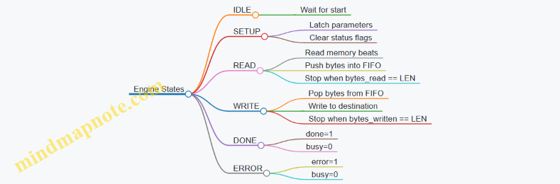
Handling Partial Transfers
Partial lengths are where bugs hide. If LEN is not a multiple of the bus word size, the last bus read/write will include unused bytes.
A safe approach:
- Track bytes_remaining.
- For each bus word, only enqueue/dequeue the number of bytes that fit within remaining length.
- When packing from a read word, select only the active byte lanes.
This keeps the FIFO byte stream aligned with the intended byte order.
Example: Deterministic Testbench Checks
In simulation, verify behavior at the register and data levels.
- After CTRL.start, STATUS.busy becomes 1 within a bounded number of cycles.
- The engine completes exactly when bytes_written reaches LEN.
- Destination memory matches source memory for the first LEN bytes.
- Bytes beyond LEN remain unchanged.
If you include error injection (like forcing a bus error response), confirm that STATUS.error is set and that no further writes occur after the fault.
Common Pitfalls and How to Avoid Them
- LEN unit mismatch: treat LEN as bytes everywhere, including address increment.
- Start re-triggering: ignore CTRL.start while busy, or require CTRL.start to be edge-based.
- FIFO overflow/underflow: gate reads on FIFO space and writes on FIFO non-empty.
- Word lane confusion: centralize byte-lane selection in one helper function so both read and write paths use the same mapping.
A “simple buffer” DMA engine is mostly about disciplined bookkeeping: clear register semantics, consistent units, and a FIFO that enforces the read/write balance. Once those are correct, the rest is just making the bus transactions obey the same rules every time.
10.5 End-to-End Bring Up Using a Minimal Software Test Suite
A minimal software test suite is the smallest set of programs that can prove the whole chain works: reset behavior, boot execution, memory map correctness, bus transactions, peripheral register semantics, and interrupt wiring. The goal is not to test everything at once; it is to test the critical path in a way that makes failures obvious.
Foundational Assumptions
Start by agreeing on three invariants between hardware and software:
- Boot address and memory map: the CPU reset vector points to a known location in RAM, and RAM is actually reachable over the SoC interconnect.
- UART output path: a single UART transmit register is mapped at a fixed address, so software can report progress.
- Register access semantics: reads and writes to peripheral registers follow the same width, alignment, and endianness expectations.
A practical rule: if you cannot print “I reached step N” from software, you cannot trust any later conclusions.
Minimal Test Suite Plan
Use a staged approach where each stage depends on the previous one.
Stage 0: Boot and Stack Sanity
- Software prints a banner.
- It writes a known pattern to a stack-local variable and reads it back.
- It performs a simple function call to ensure the calling convention and return address handling are correct.
Stage 1: Memory Reachability
- Software writes a pattern to a few RAM addresses spaced across the expected region.
- It reads them back and prints the first mismatch address.
- It also writes to a peripheral register that should be read/write and confirms the value sticks.
Stage 2: Bus Transaction Behavior
- Software performs a small sequence of reads and writes to the same peripheral register.
- It checks that read-after-write returns the last written value.
- If your peripheral has status bits, it verifies that status changes only when expected.
Stage 3: Interrupt Wiring and Trap Handling
- Software enables a single interrupt source.
- It triggers the interrupt using a control register write.
- It verifies that the trap handler runs and that the cause value matches the expected interrupt.
Stage 4: End-to-End Peripheral Exercise
- Software uses the UART to send a fixed string.
- It optionally echoes received characters if RX is implemented.
- It prints a final “PASS” only after all earlier checks succeed.
Mind Map: Bring Up Flow
Example: Stage 1 Memory and Register Checks
Below is a compact C-style sketch showing the structure. Keep it deterministic: no loops with variable bounds, no timing assumptions.
#define UART_TX_ADDR 0x10000000
#define TEST_RAM_BASE 0x80000000
#define RW_REG_ADDR 0x20000000

static void uart_putc(char c) {
  volatile unsigned int *tx = (unsigned int*)UART_TX_ADDR;
  *tx = (unsigned int)c;
}

static void uart_puts(const char *s) {
  while (*s) uart_putc(*s++);
}

static int check_word(unsigned int *addr, unsigned int expect) {
  unsigned int got = *addr;
  return got == expect;
}

int main(void) {
  uart_puts("S0\n");
  uart_puts("S1\n");

  unsigned int *p0 = (unsigned int*)TEST_RAM_BASE;
  unsigned int *p1 = (unsigned int*)(TEST_RAM_BASE + 0x100);
  *p0 = 0xA5A5A5A5; *p1 = 0x5A5A5A5A;

  if (!check_word(p0, 0xA5A5A5A5)) { uart_puts("RAM0 FAIL\n"); return 1; }
  if (!check_word(p1, 0x5A5A5A5A)) { uart_puts("RAM1 FAIL\n"); return 1; }

  volatile unsigned int *rw = (unsigned int*)RW_REG_ADDR;
  *rw = 0x12345678;
  if (*rw != 0x12345678) { uart_puts("RW REG FAIL\n"); return 1; }

  uart_puts("S2\n");
  uart_puts("PASS\n");
  while (1) {}
}
Example: Stage 3 Interrupt Verification Strategy
Make the interrupt test self-reporting. The trap handler should print the trap cause and a small signature value stored in a known RAM location. That signature lets you confirm the handler executed even if UART output is partially broken.
A simple convention:
- Before enabling interrupts, write
0xC0DE0001totrap_sig. - In the trap handler, overwrite it with
0xC0DE0002. - After returning (or after a controlled halt), software reads
trap_sigand prints whether it changed.
Practical Debug Mapping from Failure to Likely Cause
When Stage 1 fails, the most common culprits are:
- Wrong RAM base in software or wrong reset vector in hardware.
- Address map mismatch between LiteX-generated interconnect and software linker script.
- Bus width or alignment mismatch causing partial writes.
When Stage 3 fails, focus on:
- Interrupt enable bits and privilege mode expectations.
- Interrupt cause encoding in the SoC interrupt controller.
- Reset sequencing so the interrupt controller is alive when software enables interrupts.
Completion Gate
Only print the final PASS after all stages succeed. If you print PASS early and later stages fail, you lose the ability to correlate a specific failure with a specific hardware subsystem. Deterministic output is your friend; it turns “it doesn’t work” into “Stage 2 failed at RW read-after-write.”
11. Debugging Methodologies for RISC-V SoCs on FPGA
11.1 Triaging Boot Failures Using UART and CSR Reads
Boot failures are usually boring in the best way: a small set of causes repeats. The goal is to narrow from “it doesn’t boot” to a specific stage such as reset, instruction fetch, memory access, or trap handling. This section uses UART output plus CSR reads to build a tight evidence trail.
Foundational Triage Loop
Start with a loop you can run every time:
- Confirm reset and clock sanity by checking that UART prints anything at all.
- Identify the last printed milestone to determine which boot stage you reached.
- Read a small set of CSRs to learn whether the core is trapping and why.
- Correlate trap cause with memory map and bus behavior.
- Make one change at a time and repeat.
A practical milestone scheme is to print a single character per stage (e.g., R for reset entry, B for bootloader start, M for memory init, S for stack ready). If you only have one UART line, this keeps output readable.
UART Evidence That Actually Helps
UART output can lie if it’s configured wrong, so treat it as a measurement with constraints.
- Baud rate mismatch often produces garbage characters, not silence. Silence usually means the UART TX path is not clocked, pins are wrong, or reset never released.
- Early prints should avoid interrupts and avoid relying on initialized RAM. If your UART driver uses a memory-mapped register, ensure that register address is correct even before
.bssis cleared. - Print before and after risky operations. For example, print
Mbefore writing memory controller registers, then printmafter. Ifmnever appears, the fault likely occurs during those writes.
CSR Reads for RISC-V Boot Failures
When the core traps, the CSRs tell you what happened. Use a minimal trap handler that prints the CSRs once, then halts.
Read these CSRs:
mcause: the reason for the trap.mepc: the program counter at the trap.mtval: extra fault information for some causes.mstatus: whether interrupts and privilege bits are in expected states.
A simple trap handler prints mcause, mepc, and mtval in hex. If you can’t print hex yet, print decimal for mcause and raw hex for mepc.
Example: Minimal Trap Handler Pattern
// Pseudocode style for clarity
void trap_handler(void) {
  uint32_t cause = read_csr_mcause();
  uint32_t epc   = read_csr_mepc();
  uint32_t tval  = read_csr_mtval();

  uart_puts("T\n");
  uart_puts("mcause="); uart_put_hex(cause); uart_puts("\n");
  uart_puts("mepc=");   uart_put_hex(epc);   uart_puts("\n");
  uart_puts("mtval=");  uart_put_hex(tval);  uart_puts("\n");

  while (1) { /* halt */ }
}
Interpreting Common mcause Outcomes
Use mcause plus mepc to decide where to look.
- Instruction access fault:
mepcpoints to an address in flash/ROM region. If your SoC memory map is wrong, the core fetches from unmapped space and traps immediately. - Load/store access fault:
mepcpoints to the instruction that touched memory. If it happens right after stack setup, your stack region might overlap an unmapped area. - Illegal instruction:
mepcpoints to code that the core can’t decode. This often comes from using the wrong ISA variant in the software build, or from jumping into data. - Machine timer interrupt: if you see timer interrupts before you expect them, you may have enabled interrupts too early or left timer configuration active.
Mind Map: Boot Failure Triage Using UART and CSRs
Boot Failure Triage Mind Map
Example: From mepc to the Exact Bug
Suppose UART prints R then T, and the trap handler prints:
mcause = instruction access faultmepc = 0x00000000mtval = 0x00000000
This combination strongly suggests the core tried to fetch at address zero. The most common fixes are:
- Reset vector mismatch: your hardware reset PC doesn’t match the software entry point.
- Linker script mismatch: the binary is linked for a different base address than the SoC uses.
- ROM/flash mapping missing: the bus interconnect doesn’t route instruction fetches to the memory region.
After changing the reset PC or linker base, rerun and confirm that the next milestone prints before the trap.
Systematic Checklist for the Next Iteration
- Ensure UART prints at least one character before any memory clearing.
- Confirm trap handler is installed before enabling interrupts.
- Keep a stable set of milestone characters so you can compare runs.
- When you change hardware memory maps, rebuild software with the matching base.
- Use
mepcto identify the failing instruction, not just the failing stage.
This approach turns boot debugging into a sequence of small, checkable statements. The UART tells you where you are, and the CSRs tell you why you stopped.
11.2 Diagnosing Bus Errors With Transaction Level Tracing
Bus errors usually show up as “something didn’t respond” rather than “here is the exact failing signal.” Transaction-level tracing fixes that by recording intent—reads, writes, bursts, and responses—at the bus boundary. The goal is to connect three layers: (1) what the CPU requested, (2) what the interconnect routed, and (3) what the target returned.
Foundational Model of a Bus Transaction
A simple memory-mapped bus transaction has a request phase and a response phase. In a typical register bus, the request includes address, write enable, write data, and sometimes byte enables. The response includes either read data or an error/acknowledge.
Start with a minimal mental checklist:
- Address correctness: does the address fall into the intended region?
- Routing correctness: did the interconnect select the expected slave?
- Handshake correctness: did the request get accepted and did the response return?
- Data correctness: for reads, did the returned data match the expected register behavior?
- Error semantics: did the bus signal an error, or did it silently drop the request?
Mind Map: What to Trace and Why
Building a Trace That Matches Reality
Transaction-level tracing is most useful when it logs at the same granularity as your bus protocol. For example, if your bus uses separate valid/ready handshakes, log the transaction when the request is actually accepted (valid && ready), not when valid is first asserted.
A practical trace record should include:
- Timestamp or cycle number
- Master identity (if multiple)
- Operation type (read/write)
- Address
- Byte enables
- Write data (for writes)
- Response type (ack, nack, error)
- Read data (for reads)
- Slave select result (which target was chosen)
Even if you only have one master, logging “slave select result” prevents a lot of guesswork. If the interconnect chose the wrong slave, the rest of the investigation becomes straightforward.
Example: A Read That Returns an Error
Assume software reads a UART status register at 0x1001_0004 and gets an error response.
A transaction trace might show:
- CPU issues READ to
0x1001_0004with byte enables0b1111 - Interconnect decodes address and selects slave
GPIOinstead ofUART - GPIO returns an error because that offset is unmapped
From there, the fastest fix is to compare the UART base address and the interconnect’s address map. In LiteX-style systems, this often comes down to one of these:
- The UART base constant in software doesn’t match the generated CSR map
- The interconnect region boundaries are off by a power-of-two
- The address alignment assumption differs between software and hardware
A good trace makes the mismatch obvious because it shows the selected slave, not just the error.
Example: A Write That “Succeeds” But Does Nothing
Now consider a write to a control register where the trace shows an ack, but later reads show the old value.
A transaction-level trace can reveal whether the write reached the intended slave and whether byte enables were correct:
- CPU issues WRITE to
0x1000_2000with byte enables0b0011 - Interconnect routes to
TIMER - Slave acknowledges the write
- Later read returns unchanged upper bits
This pattern points to byte-enable handling. Many register blocks treat byte enables as “which bytes are valid,” so software must write the correct mask for the field width. If your register expects word-aligned writes but software writes halfwords, the trace will show the partial byte enables.
Advanced Correlation: Ordering and Reset Effects
When the bus supports pipelining, multiple transactions can be in flight. If you lack a transaction ID, you can still correlate using address and cycle ordering, but you must be careful.
Two common advanced issues:
- Out-of-order responses: the trace may show response for a later request arriving first, which can confuse software if it assumes strict ordering.
- Reset divergence: the interconnect may reset differently from the slave, causing the first transaction after reset to be routed incorrectly or dropped.
To catch both, include cycle numbers and log the first few transactions after reset release. If the first transaction consistently fails while later ones succeed, you likely have a reset sequencing or ready/ack initialization issue.
Practical Workflow for Fast Convergence
- Reduce the failing software to a single bus transaction loop that triggers the error deterministically.
- Capture a short trace window around the failure, including reset release.
- Identify the first failing transaction by response type or missing response.
- Compare expected slave selection against the trace’s slave select result.
- If routing is correct, inspect byte enables and data width handling in the target register logic.
- Fix the mismatch and rerun the same minimal test to confirm the trace now shows correct routing and response.
Transaction-level tracing turns “bus error” into a concrete story: request details, routing decision, and response outcome. Once you can see those three pieces in one place, the remaining work is usually a small, local correction rather than a full system mystery.
11.3 Handling Reset Sequencing Issues Across Clock Domains
Reset bugs across clock domains usually show up as “it boots on the bench but not on the board,” or “it works until you add one more peripheral.” The core problem is simple: a reset signal is not a single event when multiple clocks are involved. It becomes a timing relationship you must control.
Start by separating reset into three categories. First is global reset: the signal that originates from an external source or power-on reset. Second is synchronization reset: the version that is safely transferred into each clock domain. Third is functional reset: the point where logic actually releases internal state machines, FIFOs, and bus bridges.
A practical rule: only the global reset is asynchronous. Every other reset release should be synchronous to the receiving clock. If you release functional reset directly from a global reset, you are effectively asking metastability to become your system’s scheduler.
Foundational Concepts
In each clock domain, implement a reset synchronizer that converts the asynchronous global reset into a clean, clocked reset. Use at least two flip-flops for the synchronizer path. Then, add a small counter or shift register to stretch the reset long enough for downstream logic to settle. This is not superstition; it covers real-world delays such as PLL lock time, clock gating effects, and bus fabric propagation.
Also decide whether your design uses active-high or active-low reset consistently. Mixing polarities across domains is a common source of “why is everything stuck?” moments.
Reset Release Ordering
Clock-domain crossing means reset ordering is not automatic. If a peripheral depends on a bus bridge, you must ensure the bridge is ready before the peripheral starts responding to transactions. A clean approach is to define a reset dependency graph:
- Domain A hosts the bus fabric.
- Domain B hosts a peripheral.
- Domain B must remain in functional reset until Domain A has released its bus interface and any required configuration registers are stable.
Implement this with a handshake-like release: Domain A exports a “ready” flag that is synchronized into Domain B. Domain B uses that flag to gate its functional reset release.
Example: Two Clock Domains with Safe Release
Assume clk_bus drives the SoC interconnect and clk_periph drives a UART-like peripheral. Global reset is rst_n_global (active-low).
// clk_bus domain
reg [1:0] rst_sync_bus;
always @(posedge clk_bus or negedge rst_n_global) begin
  if (!rst_n_global) rst_sync_bus <= 2'b00;
  else rst_sync_bus <= {rst_sync_bus[0], 1'b1};
end
wire rst_bus = ~rst_sync_bus[1];

// clk_periph domain
reg [1:0] rst_sync_periph;
always @(posedge clk_periph or negedge rst_n_global) begin
  if (!rst_n_global) rst_sync_periph <= 2'b00;
  else rst_sync_periph <= {rst_sync_periph[0], 1'b1};
end
wire rst_periph_sync = ~rst_sync_periph[1];

// ready flag from bus domain synchronized into periph domain
// ready_bus is asserted in clk_bus after bus fabric is stable
// ready_bus_sync is a 2FF sync in clk_periph
wire rst_periph_func = rst_periph_sync | ~ready_bus_sync;
In this structure, rst_periph_func is the only reset that peripheral logic uses. The synchronizer reset (rst_periph_sync) handles metastability safety, while the ready_bus_sync term handles ordering.
Mind Map: Reset Across Clock Domains
Systematic Debug Checklist
When something fails, avoid guessing. First, confirm that each clock domain has a reset synchronizer and that functional reset is derived from the synchronized reset, not the global one. Second, check whether any bus-facing module can accept transactions before its internal state is initialized. Third, verify that any CDC FIFO or handshake has a defined reset behavior on both sides.
A useful technique is to instrument reset state in each domain. For example, expose a register bit that indicates “functional reset released” in that domain. Then you can correlate UART logs or bus reads with the actual reset timeline.
Finally, test with non-ideal timing in simulation. Randomize the relative phase between clk_bus and clk_periph, and vary the cycle at which the global reset deasserts. If your reset scheme is correct, the system should converge to the same functional behavior every time, even when the clocks disagree about when “now” is.
11.4 Interpreting Mismatches Between Simulation and Hardware
Simulation and FPGA bring-up disagree for predictable reasons: timing, reset behavior, bus semantics, and “it was fine in the testbench” assumptions. The goal is to turn mismatches into a short list of concrete causes, then confirm each with a targeted observation.
1) Start with a Mismatch Taxonomy
First classify what kind of mismatch you see. This prevents you from chasing the wrong layer.
- Functional mismatch: wrong values, wrong control flow, or missing interrupts.
- Temporal mismatch: values are correct but appear too early/late, or handshakes never complete.
- Protocol mismatch: ready/valid, byte enables, burst assumptions, or address alignment.
- Initialization mismatch: registers differ after reset, CSRs read as unexpected, or memory contents aren’t what software expects.
A quick rule: if the symptom changes when you add delays in software, you likely have a timing or reset sequencing issue. If it changes when you change bus widths or endianness handling, you likely have a protocol or mapping issue.
2) Confirm the “Same System” Assumption
Many mismatches come from building different configurations.
- Ensure the same memory map is used by both simulation and FPGA builds.
- Ensure the same software image is loaded and placed at the same address.
- Ensure the same reset strategy is applied: synchronous vs asynchronous, and whether reset is asserted long enough for all clock domains.
Example: if your simulation uses a model that initializes BRAM to zeros, but FPGA BRAM powers up unknown, your first few loads can differ even when the RTL is correct.
3) Compare Signals at the Right Boundary
Don’t compare internal RTL signals first. Compare at boundaries where behavior is specified.
- CPU-to-bus: instruction fetches, load/store transactions, and exception vectors.
- Bus-to-peripheral: register reads/writes, byte enables, and interrupt lines.
- Peripheral-to-world: UART TX/RX framing, GPIO direction, and timer tick sources.
If the CPU sees the same bus responses in hardware and simulation, but software still fails, the issue is likely in the peripheral’s external interface or in how software interprets returned data.
4) Use a Deterministic “Handshake Lens”
For bus protocols, mismatches often reduce to one of these:
- Ready/valid misuse: a master assumes the slave is ready when it isn’t.
- Combinational loops: simulation tolerates zero-delay paths that violate FPGA timing.
- Stale data: a peripheral updates read data one cycle later than the bus expects.
5) Timing and Reset: The Usual Culprits
Simulation often runs with ideal timing: zero propagation delay, perfect scheduling, and immediate reset effects. FPGA adds real delays and metastability risk.
- Reset synchronizers: if a peripheral deasserts reset earlier than the bus fabric, it may miss the first transaction.
- Clock domain crossings: a signal that is stable in simulation may violate setup/hold in hardware.
- Stalls and backpressure: a bus transaction that completes in one cycle in simulation may take multiple cycles in hardware.
Example: a UART status register that simulation updates immediately after a write might, in hardware, update after a clocked pipeline stage. Software that polls too aggressively can observe “old” status and assume the write failed.
6) Protocol Details That Bite
Even when values are “close,” protocol mismatches can break software.
- Byte enables: if your bus supports subword writes, confirm the peripheral honors
selbits. A common failure is updating the full word on a byte write. - Alignment: confirm how unaligned accesses are handled. If simulation silently supports them but hardware traps or splits them, software behavior diverges.
- Endianness: RISC-V is little-endian; ensure your peripheral register packing matches.
Example: a GPIO register block that maps bit 0 to the MSB in one environment will still look plausible in a waveform, but software will toggle the wrong pins.
7) Evidence Loop with Minimal Reproduction
Once you have a hypothesis, reduce the system until the mismatch remains.
- Disable unrelated peripherals.
- Replace complex DMA-like logic with a single register read/write path.
- Use a minimal software test that performs one operation and checks one expected value.
Then instrument the boundary signals you identified earlier. If you can’t observe internal signals easily on FPGA, observe what software observes: UART logs, CSR reads, and interrupt counts.
8) A Practical Debug Checklist
Use this sequence to avoid random changes:
- Verify build parity: memory map, software image, and reset configuration.
- Classify mismatch type: functional vs temporal vs protocol vs initialization.
- Compare boundary behavior: CPU-to-bus and bus-to-peripheral.
- Check handshake timing: ready/valid and read-data latency.
- Check reset sequencing across clock domains.
- Confirm byte enable and alignment rules.
- Create a minimal repro and change one variable at a time.
When you follow the checklist, mismatches stop being mysterious. They become a set of measurable differences between what the specification implies and what the hardware actually does.
11.5 Creating Targeted Reproduction Steps for Fast Fixes
Fast fixes start with fast, repeatable reproduction. The goal is not to “find the bug,” but to create a small, deterministic path from a change to an observable failure. When you can reproduce in minutes, you can afford to test hypotheses instead of guessing.
Foundations for Reproduction That Actually Repeats
Begin by freezing the environment and the symptom. Record the exact build inputs (HDL commit, SoC configuration, tool versions, FPGA bitstream name) and the exact failure signature (UART line, register value mismatch, timeout location, or assertion text). If the failure is timing-sensitive, capture the conditions that influence it: clock frequency, reset length, and whether the board was power-cycled or warm-reset.
Next, reduce the system until the failure still appears. A common pattern is to remove peripherals one at a time, keeping the bus fabric and the CPU running. If the failure disappears, you learned something: the removed peripheral likely perturbs timing, address decoding, or interrupt routing. If it remains, the fault is probably in CPU integration, memory map, or reset/clock discipline.
Finally, define a “reproduction script” that a teammate can run without interpretation. The script should include: which bitstream to flash, how to power/reset, what software image to run, and what exact observation proves success or failure.
Mind Map: Reproduction Steps
A Practical Template You Can Copy
Use this structure for every bug report and every fix attempt.
- Reproduction Preconditions
- Hardware: board revision, clock source, power method.
- FPGA: bitstream filename and build command.
- Software: binary name and boot address.
- Execution Steps
- Flash bitstream.
- Power cycle.
- Start software (automatic boot or manual trigger).
- Expected Result
- Example: “UART prints
BOOT_OKthenCSR_MEIP=0.”
- Example: “UART prints
- Actual Result
- Example: “UART prints
BOOT_OKthen hangs beforeCSR_MEIP.”
- Example: “UART prints
- Evidence Capture
- UART log snippet.
- Register dump if available.
- Any assertion text from simulation.
Example: Reset Sequencing Bug in a UART Bring-Up
Symptom: UART prints the first character, then stops. Sometimes it works after a warm reset.
Targeted reproduction steps:
- Preconditions: fixed bitstream, fixed UART baud setting, and a known reset source.
- Execution steps:
- Power cycle the board.
- Wait exactly 2 seconds after power-on.
- Observe UART for 5 seconds.
- Repeat 5 times with no changes.
- Expected result:
BOOT_OK, then periodicHEARTBEAT. - Actual result:
BOOT_OKappears, butHEARTBEATnever does after the first attempt.
Reduction: Temporarily disable the timer peripheral that generates HEARTBEAT, leaving UART and the bus intact. If the UART still stops, the issue is likely in reset/clock gating around the UART module or its bus interface. If UART remains stable, the timer-to-interrupt path is the culprit.
Instrumentation: Add two UART breadcrumbs around the UART transmit enable logic: one right after reset release, one after the first bus write to the UART control register. If the second breadcrumb never appears, the software likely cannot complete the control write due to bus stalls or address decoding.
Example: Bus Address Decode Mismatch
Symptom: Software writes to a GPIO register, but reads back zero.
Targeted reproduction steps:
- Preconditions: fixed memory map configuration and a minimal software test that performs only GPIO write then read.
- Execution steps:
- Boot the minimal test.
- Capture UART output for the two read values.
- Repeat 3 times.
- Expected result: readback equals the written value.
- Actual result: readback is always zero.
Reduction: Keep only the GPIO peripheral and the bus interconnect; remove other peripherals. If the mismatch persists, focus on address alignment and register offsets. If it disappears, the conflict is likely an overlapping address range or an interrupt/status register side effect.
Evidence comparison: In simulation, log bus transactions for the GPIO address range and compare them to the hardware register probe values. The reproduction script should specify the exact address used by the software and the exact register offset expected by the HDL.
Validation Loop That Prevents “Fixes” Without Proof
After each change, rerun the same reproduction script and compare the evidence, not just the symptom. If the failure signature changes (for example, from a hang to a different UART line), treat that as progress and update the symptom definition. If the failure disappears, confirm it by running the script multiple times under the same power/reset conditions.
A good reproduction step set is small, deterministic, and evidence-driven. It turns debugging from a scavenger hunt into a controlled experiment—where the board, the software, and the RTL all agree on what “happened.”
12. Packaging Open Hardware Artifacts for Collaboration
12.1 Organizing Repository Structure for RTL SoC and Software
A repository that mixes RTL, generated artifacts, simulation models, and software can still be tidy if you treat it like a build system first and a code archive second. The goal is simple: anyone should be able to clone the repo, run the documented commands, and reproduce the same outputs without guessing where files live.
Foundational Layout Principles
Start with four rules.
- Separate source from generated output. Chisel and LiteX often produce Verilog, headers, and memory maps. Keep those under a dedicated generated directory so you never edit them by accident.
- Make build products disposable. Anything produced by synthesis, simulation, or compilation should be safe to delete and regenerate.
- Keep software and hardware interface definitions close. If the CPU talks to a UART at a specific address, the address should be defined in one place and consumed by both sides.
- Use a single “top” build entry point. A newcomer should not need to learn five different command styles.
Suggested Repository Structure
Use a layout like this.
rtl/— hand-written Chisel modules, wrappers, and any custom RTL.soc/— LiteX SoC construction code and configuration scripts.sw/— bare-metal software, startup code, and linker scripts.common/— shared definitions such as register field enums, address constants, and formatting helpers.sim/— Verilator testbenches, harnesses, and simulation-specific utilities.scripts/— build orchestration, packaging, and validation helpers.docs/— human-readable notes, interface summaries, and runbooks.generated/— Chisel Verilog, LiteX headers, memory maps, and any derived artifacts.build/— intermediate build outputs from tool runs.out/— final deliverables such as bitstreams, ELF binaries, and logs.
At the repository root, include:
Makefileorjustfileas the single entry point.README.mdwith a minimal “clone and run” section.LICENSEandCONTRIBUTINGif collaboration matters.
Interface Definitions That Don’t Drift
A frequent failure mode is mismatched register addresses between hardware and software. Prevent it by generating software-visible headers from the same source used by the SoC.
A practical pattern:
- Hardware side produces a register map file under
generated/. - Software side includes a generated header under
generated/or copies it intosw/include/during the build. - Both sides also keep a human-readable summary under
docs/.
Example: a UART base address and register offsets.
- In LiteX configuration, define the UART CSR base and offsets.
- During build, emit
generated/software_regs.h. - In
sw/, include that header and use constants rather than hard-coded numbers.
Build Orchestration and Determinism
Your scripts should follow a predictable order: generate → compile → simulate → synthesize → validate.
A minimal command flow might look like:
make generatecreates Verilog and headers.make simruns Verilator with a fixed seed and captures logs.make swbuilds the ELF using the generated header.make fpgaruns synthesis and produces a bitstream.make validateruns the hardware test script and stores results underout/.
Keep the outputs timestamped or build-stamped, but do not rely on timestamps for correctness. Instead, stamp with a commit hash and tool versions captured in logs.
Mind Map: Repository Organization
Example: Directory-Level “Ownership”
When a file changes, it should be clear who owns it.
- If you change a UART register field width, update the Chisel/LiteX definition under
rtl/orsoc/, then regenerate headers intogenerated/. - If you change a software driver, update
sw/and ensure the build step pulls the latest generated header. - If you change a simulation assertion, update
sim/and keep it independent of synthesis-only constraints.
This separation keeps reviews focused: hardware changes shouldn’t require software edits unless the interface truly changed.
Example: Naming Conventions That Reduce Confusion
Use consistent naming so paths communicate intent.
generated/*.vfor Verilog outputs.generated/*.hfor software-visible headers.out/bitstreams/<board>/for bitstreams.out/logs/<target>/for simulation and validation logs.
If you include a build stamp, store it in out/BUILD_INFO.txt with the commit hash and tool versions, for example from a build performed on 2026-03-11.
Practical Checklist for a Clean Clone
After cloning, a reader should be able to:
- run
make generateand see new files appear only undergenerated/; - run
make swand confirm the software includes generated headers; - run
make simand see logs underout/; - run
make fpgaand find the bitstream underout/bitstreams/; - run
make validateand get a pass/fail summary plus captured logs.
If any step writes into rtl/, soc/, or sw/, treat it as a bug in the build hygiene.
12.2 Including Build Scripts and Exact Tool Version Notes
A release is only reproducible if the build inputs are pinned and the build steps are scripted. This section focuses on two artifacts that make collaboration boring in the best way: (1) build scripts that encode the exact command sequence, and (2) tool version notes that record what produced the results.
Build Scripts That Encode the Whole Command Sequence
Start by treating the build as a pipeline with explicit stages. Each stage should have a single responsibility, a predictable working directory, and a clear output location.
Recommended stage layout
- Generate: Chisel emits Verilog and any parameterized artifacts.
- Assemble: LiteX builds the SoC, memory map, and top-level integration.
- Simulate: Verilator runs cycle-accurate checks and produces logs.
- Synthesize: FPGA tool consumes constraints and produces reports.
- Package: Bitstream and metadata are copied into a release folder.
Best practice: scripts should fail fast. If a required environment variable is missing, stop immediately with a readable message. If a tool returns a nonzero exit code, don’t keep going.
Example: Minimal Build Script with Pinned Outputs
#!/usr/bin/env Bash
set -euo pipefail

ROOT="$(cd "$(dirname "${BASH_SOURCE[0]}")" && pwd)"
OUT="$ROOT/out"
mkdir -p "$OUT"

: "${CHISEL_VERSION:?Set CHISEL_VERSION in your environment}"
: "${LITEX_VERSION:?Set LITEX_VERSION in your environment}"
: "${VERILATOR_VERSION:?Set VERILATOR_VERSION in your environment}"

echo "[1/5] Generate"
make -C "$ROOT" generate OUT_DIR="$OUT"

echo "[2/5] Assemble"
make -C "$ROOT" soc OUT_DIR="$OUT"

echo "[3/5] Simulate"
make -C "$ROOT" sim OUT_DIR="$OUT" VERBOSE=1

echo "[4/5] Synthesize"
make -C "$ROOT" fpga OUT_DIR="$OUT" TARGET_FPGA="${TARGET_FPGA:-"unknown"}"

echo "[5/5] Package"
make -C "$ROOT" package OUT_DIR="$OUT"
This script is intentionally strict: it creates a single output root, passes it through every stage, and forces version variables to exist.
Exact Tool Version Notes That Match the Build
Version notes should be stored as a file inside the repository so they travel with the release. Use a plain text format so it’s easy to diff.
What to record
- Tool versions: Chisel, Scala, LiteX, Verilator, FPGA vendor tool, and any open-source synthesis tools you use.
- Operating system and kernel version.
- Host CPU architecture.
- Key environment variables that affect builds (for example, paths to toolchains).
- The exact commit hashes for the hardware and software repos.
- The build command lines used for the release.
Use a date for the note file that is stable for the release. For example: 2026-03-11.
Example: Tool Version Notes File
Release Notes
Date: 2026-03-11

Hardware commit: 1a2b3c4d5e
Software commit: 9f8e7d6c5b

Chisel: 3.6.0
Scala: 2.13.12
LiteX: 2024.10
Verilator: 5.022

FPGA Tool: Vendor 2024.2
Synthesis Backend: yosys 0.27

Host OS: Ubuntu 22.04.4 LTS
Kernel: 5.15.0-91-generic
Arch: x86_64

Environment
CHISEL_VERSION=3.6.0
LITEX_VERSION=2024.10
VERILATOR_VERSION=5.022
TARGET_FPGA=xc7a35ticsg324-1L

Build Commands
make generate
make soc
make sim
make fpga TARGET_FPGA=xc7a35ticsg324-1L
make package
Mind Map: Build Scripts and Version Notes
Integrated Workflow for a Clean Release Folder
When packaging, copy three things into the release directory: (1) the bitstream, (2) the synthesis and simulation reports, and (3) the version notes file. This makes the release self-describing. If someone reruns the build later, they can compare their generated reports to the saved ones without guessing which toolchain produced which result.
A small but effective rule: every script should write a short “stage summary” line into a log file under the same output root. That log becomes the breadcrumb trail that ties the version notes to the actual commands executed.
12.3 Documenting Interfaces With Register Maps and Protocol Notes
Good interface documentation lets a new person answer three questions quickly: What exists, how it behaves, and how to test it. For FPGA-based RISC-V SoCs, the most reliable “source of truth” is a register map paired with protocol notes that describe timing, ordering, and error behavior. This section shows a systematic way to write those documents so they match what your RTL and LiteX/Chisel integration actually do.
Register Map Foundations
Start with a single page that defines the addressing model. Specify the bus type (for example, LiteX Wishbone), the address width, and the unit of addressing (byte vs word). Then list each register with a stable offset, access type, reset value, and field breakdown.
A practical convention is to group registers by function and keep offsets contiguous within a block. For example, a UART block might have CTRL, STATUS, TXDATA, and RXDATA at offsets 0x00–0x0C. This makes it easy to spot missing registers and reduces off-by-one mistakes when software uses base addresses.
Include field-level details that software needs, not just what hardware contains. For each field, document:
- Bit positions and width
- Meaning of each enumerated value
- Side effects on read or write
- Validity conditions (for example, “write ignored when TX is busy”)
- Reset behavior
Protocol Notes That Match Real Timing
A register map tells you what; protocol notes tell you how. Keep protocol notes close to the registers they affect.
Begin with bus transaction rules: whether reads are combinational or registered, whether writes are single-cycle or may stall, and what happens on byte enables. If your interconnect can insert wait states, document how software should behave (typically by relying on the bus handshake rather than assuming fixed latency).
Next, describe ordering. If a write to TXDATA triggers transmission, state whether the write must be followed by polling STATUS.TX_EMPTY before writing the next word. If a read of RXDATA clears a flag, say so explicitly and note whether the clear occurs on read or on subsequent bus activity.
Finally, document error and corner cases. Examples include:
- Reading an empty receive FIFO returns a defined value (and whether it also clears an overrun flag)
- Writing to a read-only register is ignored or causes an error response
- Reset behavior for in-flight transactions
Mind Map: Register Maps and Protocol Notes
Example: UART Register Map with Protocol Notes
Below is a compact example that shows the level of specificity to aim for. It assumes a simple UART-like peripheral.
Register map summary
CTRL(0x00, RW, reset 0x0000)ENABLE[0] UART enableBAUD_DIV[15:8] baud divisor
STATUS(0x04, RO, reset 0x0000)TX_EMPTY[0] 1 when transmitter can accept a new wordRX_VALID[1] 1 when a received word is availableOVERRUN[2] 1 when a received word was lost
TXDATA(0x08, WO, reset 0x0000)- Writing enqueues a transmit word
RXDATA(0x0C, RO, reset 0x0000)- Reading returns the latest received word
Protocol notes
- Writes to
TXDATAare accepted only whenSTATUS.TX_EMPTYis 1; otherwise the write is ignored. STATUS.RX_VALIDis cleared whenRXDATAis read.- If
RX_VALIDis already 1 and a new word arrives,OVERRUNis set and the new word is dropped. CTRL.ENABLEgates both transmit and receive; when disabled,TXDATAwrites are ignored andRX_VALIDremains 0.
These statements are testable: software can poll TX_EMPTY, write TXDATA, then observe that TX_EMPTY toggles as expected.
Example: Minimal Software Sequences for Documentation
Document at least one “happy path” and one “corner case” sequence. Keep them short and deterministic.
Happy path example:
- Write
CTRL.ENABLE=1and setBAUD_DIV. - Poll
STATUS.TX_EMPTYuntil 1. - Write a word to
TXDATA. - Poll
STATUS.TX_EMPTYuntil 1 again, indicating the word was accepted.
Corner case example:
- Ensure
CTRL.ENABLE=1. - Do not read
RXDATAwhileRX_VALIDis 1. - Receive two words back-to-back.
- Verify
STATUS.OVERRUN=1and thatRXDATAreturns the first word.
When your register map and protocol notes agree with these sequences, integration becomes boring in the best way: fewer surprises, fewer “wait, what does read do?” moments, and faster bring-up across simulation and FPGA.
12.4 Providing Simulation and FPGA Test Instructions
This section turns “it builds” into “it behaves.” The goal is to give a reader a repeatable path from a clean checkout to evidence that the design works, using both simulation and FPGA runs. The instructions below assume a Chisel-to-Verilog flow feeding LiteX SoC generation, with Verilator for fast checks and an FPGA pipeline for final validation.
Test Instruction Principles
Start with a small, deterministic checklist. Each test instruction should specify: what to run, what files it consumes, what output to expect, and what failure looks like. Keep the steps ordered so a reader can stop early and still learn something.
A practical pattern is:
- Confirm build artifacts exist (Verilog netlist, SoC firmware image, constraints/bitstream inputs).
- Run simulation tests that isolate interfaces (bus, UART, timers, interrupts).
- Run a minimal firmware bring-up that exercises the same interfaces on hardware.
- Compare observations using the same register addresses and log formats.
Mind Map: Simulation and FPGA Test Instructions
Simulation Test Instructions
Build the Simulation Model
Run the Verilator build so the testbench can drive the SoC top. The key is to ensure the simulation uses the same generated Verilog that the FPGA flow uses.
Example command structure
# 1) Generate Verilog and SoC Artifacts Using Your Normal Build
# 2) Build Verilator model from the generated top
verilator -cc --exe --build \
  -Mdir obj_dir \
  -O3 \
  -Wall \
  -Wno-fatal \
  -CFLAGS "-DTESTBENCH" \
  path/to/top.v \
  path/to/testbench.cpp
If your project uses a Makefile, mirror these flags in the project scripts so readers do not invent their own options.
Run Interface-Focused Tests
Prefer tests that map directly to hardware-visible behavior.
- Bus read/write test: write a known value to a peripheral register, read it back, and verify byte enables and alignment.
- Interrupt test: trigger a timer or GPIO event, confirm the interrupt status bit sets, and confirm the CPU observes it via CSR reads or trap cause.
- UART test: send a byte stream and verify the peripheral echoes or updates a status register.
Example expected output format
[PASS] bus_rw: addr=0x40000010 val=0x0000002A
[PASS] uart_rx: byte=0x55 status=0x1
[PASS] irq: cause=0x8000000B pending=1
Capture Logs and Make Failures Actionable
When a test fails, the log should include:
- the failing address or signal name,
- the expected vs actual value,
- the simulation cycle count or timestamp,
- any relevant assertion message.
This turns “it failed” into “it failed at cycle 12345 when writing 0x40000010.”
FPGA Test Instructions
Program the Bitstream and Confirm Basic Signals
After programming, verify that the design is alive before running software-heavy tests.
- Confirm the board clock is stable.
- Confirm reset behavior by observing a UART banner or a status register that changes after reset deassertion.
Example UART bring-up expectation
boot: ok
hart0: running
periph: uart ready
Run Minimal Firmware That Matches Simulation Tests
The firmware should exercise the same register addresses and behaviors used in simulation.
A good minimal sequence is:
- Initialize UART for logging.
- Perform a bus register write/read loop for one or two peripherals.
- Trigger one interrupt source and confirm the CPU observes the expected cause.
- Print a final summary line with pass/fail.
Example firmware log summary
TEST bus_rw PASS
TEST irq PASS
TEST uart PASS
SUMMARY PASS
Validate with Register Probes When Available
If your FPGA setup includes a way to read internal signals (ILA, debug UART, or memory-mapped debug registers), use it to confirm the exact point of divergence from simulation.
For example, if UART characters are missing, probe the UART RX FIFO level and the interrupt pending bit at the moment the CPU reads the status register.
Evidence Checklist
To make results comparable across runs, require these items in the test instructions:
- Simulation evidence: test log with pass/fail lines and failing cycle counts.
- FPGA evidence: UART log with the same test names and a final SUMMARY line.
- Artifact identity: record the git commit hash or build ID used to generate the Verilog and bitstream.
- Configuration: list the target FPGA board, clock frequency, and firmware image name.
Example: A Single Command Flow
A reader should be able to run one “happy path” sequence.
# 1) Build everything
make all

# 2) Run Simulation Regression
make sim-regression

# 3) Program FPGA and Run Firmware
make fpga-flash
make fpga-run
If your project cannot support one command, split it into two scripts: one for simulation and one for FPGA, but keep the test names and expected outputs identical.
12.5 Preparing Release Artifacts Including Bitstreams and Reports
A release artifact is what someone else can take, verify, and trust without asking you 40 questions. For an FPGA-based RISC-V platform, that means bundling the exact hardware build outputs, the software image used to boot, and the evidence that the build passed both simulation and on-board checks.
Release Artifact Goals
Start by listing what must be reproducible and what must be auditable:
- Reproducible: the same inputs produce the same bitstream and the same simulation results.
- Auditable: a reviewer can see what changed, which tool versions were used, and which tests were run.
- Usable: a user can flash the bitstream and run the matching software without guessing addresses or UART settings.
Release Directory Layout
Use a stable directory structure so scripts and humans find things quickly.
hw/contains FPGA build outputs and constraints.sw/contains the bootable image and any memory initialization files.reports/contains logs, test summaries, and timing reports.docs/contains the register map snapshot and interface notes used for this release.meta/contains a manifest with hashes and tool versions.
A practical rule: if a file is needed to reproduce or verify, it belongs in the release tree, not in a developer’s home directory.
Hardware Artifacts to Include
For FPGA validation, include:
- Bitstream: the final
.bitor.binproduced by the vendor flow. - Constraints: the exact
.xdcor equivalent used for synthesis and implementation. - Top-level build outputs: generated Verilog from Chisel, LiteX-generated sources, and the final synthesized netlist if available.
- Timing evidence: the timing summary report and any constraint coverage notes.
If your flow produces multiple intermediate artifacts, keep them only when they help debugging. Otherwise, the release becomes a storage sink.
Software Artifacts to Include
Include the software image that matches the hardware memory map:
- Boot image: ELF and the raw binary used for flashing or for loading into memory.
- Linker script snapshot: the exact linker script or configuration that defines memory regions.
- Configuration: UART baud rate, base addresses for MMIO peripherals, and any boot parameters.
A small but effective practice is to embed a build identifier in the software and have the hardware print it over UART during boot. That makes “wrong image” issues obvious.
Manifest and Hashing
Create a manifest that records inputs and outputs. The manifest should include:
- Git commit hashes for hardware and software sources.
- Tool versions for Chisel, LiteX, Verilator, and the FPGA toolchain.
- Build parameters such as target FPGA part, clock frequency, and SoC configuration.
- Hashes (SHA-256) for the bitstream, software binary, and key reports.
This is the difference between “we think it matches” and “we can prove it matches.”
Mind Map: Release Evidence and Artifacts
Example: Minimal Manifest Content
Use a plain text manifest so it’s easy to diff and easy to parse.
release_id: riscv-fpga-2026-03-15
hw_git: 1a2b3c4d
sw_git: 9e8d7c6b
fpga_part: xc7a35ticsg324-1L
clock_hz: 100000000
chisel_version: 3.x
litex_version: 2026.1
verilator_version: 5.x
fpga_tool_version: 2026.1
bitstream_sha256: <hash>
software_bin_sha256: <hash>
reports_sha256: <hash>
Example: Report Checklist for a Clean Release
A release is “complete” when the following items exist and are consistent:
- Simulation: Verilator run completed, with a test summary showing pass counts and no unexpected X-propagation warnings.
- SoC Connectivity: at least one test confirms MMIO read/write correctness for each peripheral class.
- Boot: UART output shows the software build identifier and a known-good boot message.
- Timing: timing report shows no unconstrained paths and meets the target clock.
Packaging and Naming Conventions
Name artifacts so they encode what matters:
- Include the release id in filenames.
- Keep the bitstream and software binary names aligned to the same release id.
- Store logs with timestamps and the same release id so you can correlate them later.
A good release is boring in the best way: everything needed to flash, run, and verify is present, and the manifest tells you exactly what you’re looking at.