Arduino and ESP32 Hardware Startup Guide
1. Hardware Foundations for Arduino and ESP32
1.1 Define Hardware Requirements for an IoT Product
Start by turning “we need an IoT device” into a set of measurable hardware requirements. If you can’t measure it, you can’t test it, and if you can’t test it, you’ll end up debugging wiring at 2 a.m. (which is a terrible use of anyone’s time).
Clarify the Use Case and Operating Context
Write a short scenario that includes where the device lives and what it does. Hardware requirements change dramatically based on environment and usage pattern.
- Environment: indoor vs outdoor, dust, water exposure, vibration, temperature range.
- Power availability: always-on power, battery-only, or intermittent charging.
- Connectivity: Wi-Fi only, cellular, or local-only (for example, Bluetooth to a gateway).
- User interaction: buttons, LEDs, displays, or no direct interaction.
Example: A soil moisture node in a greenhouse needs corrosion-resistant parts, stable analog readings, and a power plan that tolerates long sleep intervals.
Translate Functions into Sensors, Actuators, and Interfaces
List every input and output the device must handle. Then map each item to an interface type and electrical behavior.
- Inputs: digital sensors (I2C/SPI/GPIO), analog sensors (ADC), pulse sensors (interrupts).
- Outputs: relays, MOSFET-driven loads, LEDs, buzzers, communication modules.
- Control signals: PWM for dimming or motor control, enable lines for power gating.
Example: If you need a barometric sensor plus a status LED, you might choose I2C for the sensor and a GPIO-controlled LED with a resistor sized for your supply voltage.
Define Performance Targets That Drive Hardware Choices
Hardware selection depends on constraints you can quantify.
- Sampling and latency: how often you measure, how quickly you react.
- Accuracy and resolution: ADC resolution needs, sensor tolerances, calibration strategy.
- Throughput: how much data you send and how often.
- Reliability: acceptable failure modes, watchdog behavior, brownout tolerance.
Example: If you must detect a threshold change within 200 ms, you need an interrupt-capable input and a firmware plan that avoids long blocking operations.
Specify Power Requirements with Realistic Load Profiles
Power requirements should include both average and peak consumption.
- Average current: determined by duty cycle (sleep time vs active time).
- Peak current: determined by radio transmit, sensor warm-up, and actuator switching.
- Battery capacity and runtime: based on expected operating schedule.
- Power rails: required voltages for MCU, sensors, and high-current loads.
Example: A device that transmits every minute may have low average current but still needs a regulator and bulk capacitance that handle radio transmit peaks without resetting.
Determine Mechanical and Environmental Requirements
Mechanical constraints affect electrical reliability.
- Enclosure: size limits, mounting holes, cable strain relief.
- Connectors: locking vs friction-fit, pin count, wire gauge compatibility.
- Ingress protection: gasket needs, conformal coating considerations.
- Thermal behavior: heat from regulators and enclosed electronics.
Example: If the enclosure is small and sealed, regulator heat and battery venting paths become part of the hardware requirements, not an afterthought.
Map Requirements to MCU Resources and Pin Budget
Before choosing a board, confirm the MCU can support your plan.
- Pin count and multiplexing: which pins support ADC, interrupts, I2C, SPI, PWM.
- Voltage domains: 3.3 V vs 5 V compatibility.
- Peripheral availability: number of I2C/SPI buses, UARTs, timers.
- Memory needs: firmware size and buffering for sensor data.
Example: If you need two I2C buses, three UARTs, and multiple PWM outputs, you may run out of usable pins on a smaller package unless you plan carefully.
Create a Requirements Checklist and Acceptance Criteria
Turn the above into a checklist you can test on a bench.
- Electrical: correct boot voltage range, stable operation under load steps, no brownouts.
- Interface: sensor communication works at the chosen bus speed and cable length.
- Performance: measurement timing and actuator response meet targets.
- Environmental: operation within temperature range and tolerance to expected exposure.
Example: Acceptance criteria might state that the device must not reset when the actuator switches on, and that sensor readings must stay within a specified error band after calibration.
Mind Map: Hardware Requirements Flow
Example: Turning Requirements into a First Draft
A practical first draft can look like this:
- Inputs: one I2C sensor, one analog sensor, one button interrupt.
- Outputs: one MOSFET-driven actuator, one status LED.
- Timing: sample every 1 s; actuator response within 200 ms after threshold.
- Power: battery-powered; average current target under 50 mA; peak current must not cause resets during radio transmit.
- Environment: 0–50°C; enclosure must handle condensation without direct water ingress.
- Connectivity: Wi-Fi for telemetry.
This draft is specific enough to guide board selection, regulator sizing, connector choice, and pin mapping—without locking you into a single part number too early.
1.2 Select the Right Development Board for Your Use Case
Choosing a development board is less about picking the “best” one and more about matching constraints: power, interfaces, timing, size, and how you plan to test and debug. A good selection reduces rework later, especially when you move from a breadboard prototype to a PCB.
Start with Your Use Case Requirements
Begin by writing down what the board must do, not what you hope it will do. Use these categories as a checklist:
- Compute and timing needs: Does your firmware need precise sampling, tight control loops, or mostly event-driven logic?
- Sensor and actuator interfaces: Which buses do you need (I2C, SPI, UART, analog ADC, PWM, CAN)?
- Power profile: Will it run from USB, a battery, or a regulated rail? How long should it last?
- Connectivity: Do you need Wi-Fi, Bluetooth, Ethernet, or only local wired links?
- Physical constraints: Board size, mounting style, and connector availability.
- Debug and bring-up: Do you have easy access to UART, JTAG, or test pads?
A practical rule: if you can’t describe your required interfaces in one sentence, you’re not ready to choose the board.
Match Board Families to Hardware Capabilities
Arduino boards are often the fastest path to a working prototype, especially when your design is simple and you want a familiar programming model. ESP32 boards add wireless capability and typically more flexible peripherals, but you must pay attention to power and boot behavior.
When comparing boards, focus on these hardware traits:
- I/O voltage levels and pin multiplexing: Some pins are fixed-function; others can be reassigned. Confirm which pins support the interfaces you plan to use.
- Analog performance: ADC resolution is only part of the story. Check input range, reference behavior, and whether you need external scaling.
- Clocking and timers: If you need stable PWM or periodic sampling, verify timer availability and how it interacts with other peripherals.
- Memory and flash: Larger firmware, file systems, or logging can require more flash than you expect.
Use a Decision Mind Map
The mind map below turns the checklist into a selection workflow.
Mind Map: Development Board Selection Workflow
Compare Boards Using a Concrete Scoring Table
Instead of vague preferences, score each board against your requirements. Here’s a compact template you can reuse.
| Criterion | What To Check | Weight | Score 0-5 |
|---|---|---|---|
| Required interfaces | Pin availability for I2C/SPI/UART/ADC/PWM | 3 | |
| Power compatibility | Input range, regulator quality, sleep support | 3 | |
| Wireless needs | Wi-Fi/BLE support and antenna constraints | 2 | |
| Timing needs | Timer/PWM capability and interrupt behavior | 2 | |
| Debug access | UART/JTAG/SWD, easy reset/boot | 2 | |
| Physical integration | Headers, mounting, connector placement | 1 |
Add the weighted scores and you’ll usually see the winner quickly. If two boards tie, the deciding factor is typically debug access or power behavior.
Example: Choosing for a Battery Sensor Node
Suppose you need a battery-powered node that reads a sensor over I2C, measures analog temperature, and sends data over Wi-Fi.
- Interfaces: You need I2C and ADC; PWM might be optional for a status LED.
- Power: Battery operation means you care about sleep modes and regulator efficiency.
- Connectivity: Wi-Fi pushes you toward an ESP32-class board.
A board with accessible I2C pins, stable ADC scaling options, and a clear power input path will reduce bring-up time. On the hardware side, plan a clean power measurement point so you can confirm current draw during active transmit and during sleep.
Example: Choosing for a Wired Industrial Prototype
Now imagine a prototype that controls a motor driver with PWM, reads a few digital inputs, and communicates over UART to a host.
- Interfaces: PWM and UART are central; I2C and ADC may be minimal.
- Connectivity: Wired only, so Wi-Fi is unnecessary.
- Debug: You want straightforward serial logs and predictable reset behavior.
In this case, an Arduino-style board can be a strong fit because it keeps the hardware surface area smaller. The key is to verify that the PWM pins you plan to use are not shared with other critical functions on that specific board.
Verify the Pinout and Power Path Before You Buy
Before committing, do two quick checks:
- Pinout mapping: Confirm that every required signal has a real pin on the board, and that the pin supports the needed peripheral mode.
- Power path sanity: Ensure your intended supply voltage matches the board’s input expectations, and that any onboard regulator can handle your load without excessive dropout.
A board that “should work” on paper often fails because of one missing pin function or a power rail mismatch. Fixing that early is cheaper than rewriting wiring after the first PCB spin.
Mind Map: Board Verification Checklist

Practical Selection Outcome
By the end of this step, you should be able to name the board family, justify it with interface and power requirements, and list the exact pins and rails you will use. That clarity is what turns “a board” into a working prototype.
1.3 Understand Core Electrical Concepts for Embedded Systems
Embedded hardware is mostly a controlled conversation between voltages, currents, and timing. If you understand the basics, you can predict what will happen when you connect a sensor, switch a load, or run a microcontroller from a battery. This section builds from the “what” to the “why it matters” for Arduino and ESP32 systems.
Mind Map: Core Electrical Concepts
Voltage: The Reference You Actually Care About
Voltage is the electrical “height” difference between two points. A multimeter reading is always relative to the probe reference, so measuring “5 V” without a shared ground can mislead you. In embedded systems, the microcontroller’s ground is the reference for almost everything: sensor outputs, ADC readings, and logic levels.
A practical check: before wiring anything, identify the board’s ground pins and confirm continuity between them. Then verify the rail voltages at the points you will power from, not just at the regulator output. A breadboard wire can drop voltage under load, and the MCU will notice.
Current: What Your Components Must Safely Carry
Current is how much charge flows per second. It’s easy to underestimate because many datasheets list “typical” currents, while startup and switching can be higher. For example, an LED with a resistor is mostly predictable (resistive load), but a motor or solenoid is not: current changes quickly and can exceed steady-state values.
When you measure current, remember the meter must be in series. If you accidentally place it across a rail, you’ll create a short circuit. That’s not a “learning experience,” it’s a smoke test.
Resistance and Ohm’s Law: Predicting Simple Loads
Ohm’s law connects voltage, current, and resistance: I = V / R. For a resistor, power dissipation is P = I^2 * R. This matters when you design current-limiting resistors for LEDs or set pull-up strengths for signals.
Example: If you run a 3.3 V LED circuit and the LED needs about 2.0 V at 10 mA, the resistor sees 1.3 V. R = 1.3 V / 0.01 A = 130 Ω. Choose a standard value like 120 Ω or 150 Ω, then verify power: P = (0.01 A)^2 * 120 Ω = 0.012 W. A 0.25 W resistor is plenty.
Power and Energy: Why Regulators Get Hot
Power is the rate of energy use: P = V * I. Regulators convert power from one voltage level to another, and the difference becomes heat. If you power an ESP32 from 5 V and draw 300 mA at 3.3 V, the output power is 0.99 W. If the regulator is 80% efficient, input power is about 1.24 W, so heat is roughly 0.25 W. That heat changes with load and ambient temperature.
A good habit is to compute worst-case regulator dissipation using the maximum expected current and the regulator’s efficiency or dropout behavior from the datasheet. Then check whether the package can handle it without relying on luck.
Ground and Return Paths: The Hidden Wiring
Ground isn’t just “0 V.” It’s the return path for currents. When high-current switching happens (like a relay coil or a MOSFET driving a motor), the return current can create voltage drops across shared traces. Those drops can show up as glitches on ADC readings or as random resets.
A systematic approach: route high-current returns separately from sensitive analog and MCU ground, then connect them at a controlled point (often near the regulator or power entry). Even on a prototype, you can reduce noise by keeping the switching loop area small and by placing decoupling capacitors close to the MCU.
Capacitance and Decoupling: Stabilizing Fast Transients
Capacitors resist sudden changes in voltage. Decoupling capacitors provide local charge so the MCU doesn’t demand current from a distant regulator every time it toggles internal logic or radio transmit power.
Example: If an ESP32 transmits, its current draw can spike. Without adequate decoupling and low-impedance power routing, the 3.3 V rail can dip, causing brownout resets. The fix is not “add a bigger battery,” it’s “reduce impedance”: place capacitors near the MCU power pins and ensure the power path is thick and short.
Inductance and Switching: Why Diodes Exist
Inductors resist changes in current. When you switch an inductive load off, the current doesn’t vanish instantly; it forces a voltage spike. A flyback diode across a coil provides a path for that current, limiting the voltage excursion.
Example: Driving a solenoid with a MOSFET without a flyback diode can create a high-voltage spike that couples into the MCU ground and damages components. With a diode, the energy is safely dissipated in the diode and coil resistance, and the MCU sees a calmer electrical environment.
Signal Integrity: Logic Levels and Pull Resistors
Digital signals depend on thresholds: a “high” must be above the input’s minimum VIH, and a “low” must be below VIL. Noise margins shrink when wiring is long or when edges are slow due to weak pull-ups.
Pull-up resistors prevent floating inputs. Floating pins can randomly read as either state because the input capacitance and leakage currents create unpredictable voltages. A simple test is to power the board and observe the pin state in firmware before connecting a sensor; if it changes when you touch wires, you’ve found a floating input.
Protection: Current Limiting and Safe Failure Modes
Protection components exist to keep faults from turning into permanent damage. Current limiting resistors, series resistors on GPIO lines, proper fusing, and ESD protection strategies reduce the impact of wiring mistakes and electrostatic discharge.
A practical workflow: before connecting a new peripheral, check for shorts between power rails and ground, verify polarity, and confirm that any signal line has a defined state through pull-ups or pull-downs. When you do connect, start with conservative settings in firmware and measure the rail voltages under load.
Example: A Quick Bring-Up Checklist
- Verify ground continuity across the system.
- Measure rail voltages at the MCU power pins under expected load.
- Confirm pull-ups or pull-downs for any input that could float.
- Add flyback protection for inductive loads.
- Place decoupling capacitors near the MCU and any fast-switching ICs.
With these concepts in place, the rest of the startup guide becomes less about memorizing steps and more about predicting electrical behavior from first principles.
1.4 Map Signals and Power Paths from Sensor to MCU
A reliable startup starts with a clear map of two things: where power comes from, and how signals travel. If you can trace both paths with a finger on the schematic, you can usually trace failures too.
Foundational Model of a Sensor Node
Think of each sensor node as four blocks: power input, signal output, optional protection, and the MCU interface. Power and signal may share grounds, but they should not share “problems.” A clean ground reference matters because most signal errors are really ground errors.
Power path goals
- Provide the sensor’s required voltage range under load.
- Keep regulator behavior stable during startup and transients.
- Ensure the sensor ground returns to the same reference point the MCU uses for that interface.
Signal path goals
- Match electrical levels and timing expectations.
- Prevent fault conditions from damaging the MCU pin.
- Control noise coupling by routing and termination choices.
Mind Map: Signal and Power Mapping
Sensor to MCU Mapping Mind Map
Step 1: Identify Power Requirements and Return Strategy
Start by writing the sensor’s power requirements in plain terms: voltage range, current draw, and any startup behavior (for example, “needs 50 ms to stabilize”). Then decide where that power rail is generated.
Example: 3.3 V sensor on a mixed system
- If your MCU is 3.3 V, power the sensor from the same 3.3 V regulator rail.
- If you must use a separate regulator, connect grounds carefully: route the sensor ground back to the MCU ground reference point used by the interface, not to the return of a motor driver.
Practical mapping checks
- Mark the sensor’s V+ pin and its GND pin on the schematic.
- Draw an explicit “return path” line from sensor GND to the chosen ground node.
- Add decoupling at the sensor: a small capacitor close to V+ and GND, plus any bulk capacitance if the sensor draws bursts.
Step 2: Map the Signal Path by Interface Type
Once power is stable, map the signal based on whether it is digital or analog.
Digital Signals
Digital interfaces care about logic levels, pull resistors, and bus integrity.
I2C example
- SDA and SCL need pull-ups to the correct logic rail.
- Place pull-ups so the bus sees a predictable rise time.
- If the sensor is far away, consider series resistors near the MCU to reduce ringing.
SPI example
- Ensure SCK, MOSI, and MISO share the same logic voltage domain.
- Treat chip select as a first-class signal: route it cleanly and avoid sharing it with noisy lines.
Analog Signals
Analog paths care about impedance, reference, and filtering.
Analog voltage sensor example
- If the sensor output can exceed the ADC range, add a resistor divider or clamp so the ADC never sees out-of-range voltage.
- Add an RC low-pass filter only if it matches your sampling rate; otherwise you’ll smear readings.
Analog current sensor example
- Convert current to voltage with a shunt resistor.
- Use a differential approach if available, or at least route the shunt sense lines as a tight pair to reduce noise pickup.
Step 3: Add Protection and Measurement Points
Protection is not optional when cables, connectors, or field wiring enter the picture.
Series resistor pattern
- Put a small series resistor on the signal line near the MCU pin for digital signals.
- It limits pin current during transients and helps tame ringing.
Clamp strategy
- Use a clamp (diode network or TVS) when the signal can be driven beyond rails.
- Ensure the clamp current has a safe return path, usually through the same ground strategy you already mapped.
Measurement points
- Add test pads for V+ at the sensor, sensor GND, and the signal at the MCU pin.
- During bring-up, you want to measure “what the MCU sees,” not just what the schematic claims.
Step 4: Validate the Mapping with a Bring-Up Sequence
A good bring-up sequence follows the map.
- Power the sensor rail alone and measure V+ at the sensor.
- Confirm sensor ground continuity and absence of large voltage drops under load.
- Probe the signal at the sensor output, then at the MCU pin.
- Only then enable the full firmware initialization.
If the signal looks correct at the sensor but not at the MCU, the problem is almost always routing, level mismatch, pull-up placement, or protection components interacting with the signal.
Example: One Page Mapping Checklist
- Sensor V+ connected to the correct rail with local decoupling.
- Sensor GND returns to the intended ground node, not the noisy return of actuators.
- Digital pull-ups reference the correct logic rail.
- Analog signals are scaled/clamped to ADC range.
- Series resistors and clamps are placed with safe current paths.
- Test pads exist for V+ at sensor, GND at sensor, and signal at MCU pin.
1.5 Plan for Mechanical Integration and Cable Management
Mechanical integration is where “it works on the bench” either becomes “it survives real handling” or turns into a slow-motion mystery. The goal is simple: keep the electronics supported, keep connectors aligned, and keep cables from becoming the weakest link.
Mechanical Integration Workflow
Start with a buildable stack: enclosure, mounting points, PCB location, sensor openings, and cable entry paths. Before you pick a cable type, decide where the strain will go. If the cable can tug on a connector, it will eventually do so—often at the worst moment.
-
Define mounting strategy: Use standoffs that match your PCB hole pattern and keep the board from flexing. If you expect vibration, avoid “floating” PCBs held only by screws at one corner.
-
Set connector access rules: Plan for how you will plug in programming cables, service connectors, and any removable sensor leads. If a connector is buried, you’ll end up removing the enclosure every time you need to troubleshoot.
-
Control enclosure openings: Cutouts for sensors and ports should be sized for the connector and the sealing method you intend to use (gasket, O-ring, or simple strain relief). A tight opening that forces the cable to bend sharply is a reliability tax.
-
Add mechanical clearances: Leave room for wire routing, connector housings, and bend radii. A common failure mode is a cable that looks fine when the enclosure is open, but gets pinched when the lid closes.
Cable Management Principles That Actually Matter
Cable management is not about neatness for its own sake. It’s about preventing stress, protecting signal integrity, and making assembly repeatable.
- Strain relief first: Terminate cable forces at the enclosure or a dedicated bracket, not at the PCB header. A simple clamp or grommet can prevent connector rocking.
- Bend radius discipline: Route cables so they never require a sharp bend near the connector. If you can feel a “kink” with your fingers, the cable will eventually complain.
- Service loop planning: Provide a small slack loop so the cable can be disconnected without pulling the entire harness out of place.
- Separation of noisy and quiet: Keep power switching wires away from analog sensor leads. If you must cross, cross at right angles and avoid long parallel runs.
- Connector orientation consistency: Mark harness sides so the same cable goes to the same header every time. Misorientation is a mechanical problem that becomes an electrical problem.
Routing Patterns for Common Arduino and ESP32 Builds
Use routing patterns that match the physical layout of the board.
- Edge-to-edge routing: For boards mounted near the enclosure wall, route cables along the enclosure perimeter. This reduces the chance of pinching and keeps the center area clear.
- Top-down harnessing: If you have a lid-mounted sensor or display, route from the PCB upward to the lid opening, then secure the cable along the lid edge.
- Central trunk with branches: Create one main harness run, then branch to sensors. This makes it easier to add or remove a sensor without reworking everything.
Strain Relief and Connector Protection
A practical approach is to treat the cable like a lever. The enclosure should absorb the lever force.
- Use grommets at entry points to prevent abrasion.
- Use tie-down points so the cable can’t move relative to the connector.
- If you use ribbon cables or flat cables, secure them so they don’t twist.
Example: Strain Relief for a Sensor Cable
You have an ESP32 board with a sensor on the enclosure wall. Route the sensor cable from the PCB to a grommeted entry, then clamp the cable to a small internal bracket before it reaches the connector. When you tug the cable, the bracket takes the force; the connector sees only the normal insertion load.
Mind Map: Mechanical Integration and Cable Management
Validation Checks Before You Call It Done
Run three quick tests with the enclosure closed:
- Pinch test: Close the lid slowly while watching the cable path. If any cable shifts or compresses, reroute or add clearance.
- Tug test: Apply gentle pull force to the cable near the entry point. The connector should not move relative to the PCB.
- Flex test: Move the enclosure slightly (within reason) and confirm the connector and solder joints don’t experience noticeable strain.
These checks are small, but they catch the mechanical issues that otherwise show up later as intermittent resets, flaky sensor readings, or connectors that “work until they don’t.”
2. Tooling Setup for Hardware Bring Up
2.1 Install Drivers and Verify USB Communication
When USB communication fails, it’s usually not the firmware. It’s the path from your computer’s USB port to the board’s USB-to-serial chip, plus the driver layer that makes the operating system expose a usable serial device. The goal of this section is to get you to a stable, repeatable “I can see the port and I can talk to it” state.
What You Need Before Installing
Start by identifying the board’s USB interface type. Many Arduino boards use a USB-to-serial chip such as CH340, CP2102, or FT232. ESP32 dev boards often use CP2102 or CH340 as well, but some use native USB on specific variants. If you don’t know which chip you have, look for markings on the USB-to-serial IC or check the board documentation printed on the PCB.
Driver Installation That Doesn’t Create Chaos
Install drivers only for the USB-to-serial chip you actually have. Installing multiple competing driver packages can cause the OS to bind the wrong driver to the device, which looks like “it connects but no serial port appears.”
A practical workflow:
- Plug the board in.
- Observe whether the OS detects a new device.
- If a serial port appears immediately, you may already be set.
- If not, install the driver for the detected USB-to-serial chip.
- Unplug and replug once to force the OS to re-enumerate.
If you’re using Windows, Device Manager is your truth source. Look under Ports (COM & LPT). If you see a COM port number, note it. If you see an “Unknown device” or a device with a warning icon, that’s your driver gap.
Verify USB Enumeration and Port Stability
USB enumeration means the OS can consistently identify the device and assign it a serial interface. Port stability means the COM port name doesn’t randomly change every time you plug in.
Do this check:
- Plug the board into the same physical USB port.
- Confirm the COM port appears.
- Open a serial monitor at the board’s default baud rate (often 9600 for many Arduino examples; ESP32 examples often use 115200).
- Trigger a simple output from the board (for Arduino, upload a “Blink” won’t print; you need a sketch that writes to Serial). For ESP32, many examples print boot logs.
If the port appears but you get garbled text, the baud rate is wrong or the board is not actually sending what you think it is.
Mind Map: USB Driver and Communication Verification
Example: Windows Driver Check and Serial Test
- Plug the board in.
- Open Device Manager.
- Confirm it appears under Ports.
- Note the COM port, for example COM5.
- Upload a sketch that prints a line every second.
Example sketch (Arduino-style):
void setup() {
  Serial.begin(9600);
  while (!Serial) { }
}

void loop() {
  Serial.println("USB link OK");
  delay(1000);
}
Then open your serial monitor:
- Select COM5.
- Set baud rate to 9600.
- You should see “USB link OK” repeating.
If you see nothing, confirm the board is powered correctly and that the upload succeeded. A successful upload does not guarantee the serial monitor is using the right port.
Example: Linux Port Discovery and Quick Sanity Checks
On Linux, the serial device often appears as /dev/ttyUSB0 or /dev/ttyACM0. After plugging in, run a check by comparing before/after device lists.
Then open a serial monitor with the correct baud rate. If you get no output, verify that your sketch actually prints and that you selected the correct device node.
Common Failure Modes and Targeted Fixes
- No serial port appears: driver missing, wrong driver bound, or the USB-to-serial chip not enumerating due to power or cable issues.
- Port appears then disappears: unstable power or a cable that only supports charging; try a known data-capable cable.
- Port appears but output is garbled: baud rate mismatch or wrong board selected in the serial monitor.
- Port number changes every plug: the OS is reassigning based on USB topology; use the same port during development to reduce confusion.
Case Study: A Clean Bring-Up on 2026-02-20
On 2026-02-20, a developer plugged an ESP32 board into a new laptop USB port. The board powered (LED on) but no COM port appeared. Device Manager showed an “Unknown device,” indicating the USB-to-serial driver was missing. After installing the driver matching the board’s CP2102 chip and replugging, a COM port appeared and the serial monitor at 115200 showed boot messages. The next step was not firmware changes; it was confirming the port remained stable across multiple replug cycles before moving on to peripheral bring-up.
2.2 Configure Serial Monitoring and Logging Workflows
Serial monitoring is the fastest way to see what your hardware is doing, but only if you treat it like a system: consistent settings, predictable message formats, and a workflow that survives both success and failure. The goal is simple—turn raw bytes into evidence you can act on.
Establish Baseline Serial Parameters
Start by locking down the basics so you can trust what you read.
- Match baud rate between the board and the monitor. If you see garbled characters, it’s usually baud mismatch, not “mystery noise.”
- Choose a line ending strategy. For human-readable logs, use newline \(
\n\) so each message becomes a complete line. - Use a single output stream for early bring-up. Mixing debug prints with binary data makes later parsing painful.
A practical baseline is: 115200 baud, newline-terminated lines, and one message per line.
Define a Logging Format You Can Parse
When logs are consistent, you can scan them quickly and also copy them into scripts later.
Use a format with:
- Timestamp or monotonic counter (even a simple counter works)
- Severity (INFO, WARN, ERROR)
- Subsystem (POWER, GPIO, I2C, SPI, BOOT)
- Message with key-value pairs
Example line:
[000123] INFO POWER vbat=4.98V rail=3v3 ok
This structure helps you answer: What happened, when, and where? without rereading the whole file.
Implement Non-Blocking, Line-Oriented Output
During startup, you want logs to appear reliably without slowing the system into weird timing. Avoid long blocking delays just to print.
A simple pattern is to print short lines and keep them newline-terminated.
static uint32_t seq = 0;
void logLine(const char* level, const char* tag, const char* msg) {
  Serial.print('[');
  Serial.print(seq++);
  Serial.print("] ");
  Serial.print(level);
  Serial.print(' ');
  Serial.print(tag);
  Serial.print(' ');
  Serial.println(msg);
}

void setup() {
  Serial.begin(115200);
  delay(50);
  logLine("INFO", "BOOT", "serial_ready");
}
If you need numbers, format them into the same line rather than printing multiple fragments. Fragmented output is how “one message” turns into three half-messages.
Create a Bring-Up Workflow That Produces Evidence
A good workflow reduces the number of times you have to guess.
- Power on with a known-good cable and supply.
- Capture logs from reset to first loop. Many hardware faults happen before your main code runs.
- Repeat with one change at a time: baud rate, pullups, wiring, regulator load.
- Record the exact settings used for the capture: baud, monitor line ending, and board revision.
For example, if I2C fails, you want to see the log line that reports the I2C initialization attempt, not only the later symptom.
Add Hardware-Aware Checkpoints
Logs become more useful when they align with hardware checkpoints.
- After power rail stabilization: print measured voltages if you have an ADC channel.
- After pin mode configuration: print which pins are inputs/outputs and any pull settings.
- After peripheral init: print success/failure codes.
This turns “it doesn’t work” into “GPIO configuration succeeded, I2C init failed with code X.”
Use Severity Levels and Stop Conditions
Severity levels prevent log spam from hiding the real issue.
- INFO: normal milestones
- WARN: recoverable oddities (e.g., sensor not detected)
- ERROR: conditions that block correct operation
A simple stop condition is to halt further peripheral attempts after an ERROR, so you don’t produce misleading follow-up messages.
Mind Map: Serial Monitoring and Logging Workflows
Example Workflow for a Failing Peripheral
Suppose a sensor on I2C doesn’t respond.
- Log
INFO I2C init_startbefore calling the I2C begin/init. - Log
INFO I2C scan_start addr=0x00..0x7Fif you perform a scan. - If no device is found, log
ERROR I2C no_ack addr=0x3C(use the actual address you tried). - Then stop further I2C-dependent actions and print
WARN APP skipping_sensor_read.
Now the log tells you whether the failure is wiring/addressing, initialization order, or a later read issue. That’s the difference between “debugging” and “diagnosing.”
2.3 Use Multimeters and Oscilloscopes for Baseline Checks
Baseline checks are the fastest way to catch “it should work” problems before you spend hours chasing firmware. The goal is simple: measure the electrical reality at power-up, during steady operation, and during the first meaningful load event.
Start with Safe, Repeatable Setup
Before measuring anything, define the test points and the power conditions you will repeat. Use a bench supply when possible, and keep a current limit set low enough to prevent component damage while you learn the circuit’s behavior.
A practical baseline workflow:
- Visual inspection: connector orientation, polarity marks, and obvious shorts.
- Power rails check: confirm each rail reaches its expected voltage.
- Ground reference check: verify the “0 V” you probe is the same node your circuit uses.
- Dynamic check: observe what changes when the MCU boots and when a peripheral turns on.
Multimeter Measurements That Matter
A multimeter is great for DC truth and continuity sanity.
Voltage rail verification
- Measure each regulator output at the load side, not just at the regulator pin.
- If a rail is low, check whether the regulator is in dropout, current-limited, or oscillating.
Continuity and resistance checks
- With power off, confirm there are no shorts between rails and ground.
- For series resistors and fuses, verify they match expected values within tolerance.
Diode and transistor checks
- Use diode mode to identify swapped components or reversed protection diodes.
- For MOSFETs, confirm body diode orientation so you don’t discover it the hard way during power-on.
Example: catching a swapped regulator output If a 3.3 V rail reads 0.8 V with power applied, measure the regulator input and enable pin. If input is correct but output is low, check enable wiring and any feedback divider. A swapped feedback resistor often produces a stable but wrong voltage—multimeters catch that immediately.
Oscilloscope Measurements That Matter
An oscilloscope shows what the multimeter averages away: transients, ringing, and timing.
Probe discipline
- Use short ground leads or spring tips to reduce noise pickup.
- Set the scope to the correct voltage scale and trigger source before powering the circuit.
Boot transient capture
- Trigger on the rising edge of the main 3.3 V rail.
- Capture at least 200 ms if your system boots slowly, or shorter if it’s quick.
- Look for dips below brownout thresholds and for slow ramp behavior.
Ripple and noise
- Switch the scope to AC coupling to see ripple riding on a rail.
- Measure ripple amplitude during steady state and during load events.
Example: identifying brownout causes If the MCU resets repeatedly, capture the 3.3 V rail during the first peripheral activation. A brief dip from 3.3 V to 2.7 V that lasts a few milliseconds can be enough to trigger brownout. The multimeter might show “3.3 V” because it averages; the scope shows the dip.
Mind Map: Baseline Checks with Instruments
Systematic Troubleshooting with Measurements
Use measurements to narrow the fault domain.
- If a rail is missing on the multimeter: stop and fix power distribution first. No amount of firmware can compensate for a rail that never reaches threshold.
- If rails are correct but behavior is unstable: focus on transient events. Capture the rail while the MCU boots and while the first load turns on.
- If resets correlate with a peripheral: measure the rail at the MCU power pins and at the peripheral supply pins. A voltage drop that appears only near the peripheral often indicates wiring resistance or inadequate local decoupling.
Example: A Two-Stage Baseline Test
Run two captures so you can compare “quiet” and “busy” behavior.
- Stage A: MCU boot only
- Scope trigger on 3.3 V rise.
- Measure ramp time, overshoot, and any dips.
- Stage B: MCU boot plus first peripheral enable
- Identify the moment firmware turns on the peripheral.
- Capture the same rail and note the dip depth and duration.
If Stage B shows a deeper dip than Stage A, you’ve proven the issue is load-related. The next step is to measure current draw and check the power path and decoupling near the load.
Practical Baseline Checklist
- Power rails reach expected values at the load side
- No rail-to-ground shorts with power off
- Scope shows stable ramp and no brownout dips during boot
- Ripple is reasonable in steady state
- Load events do not cause unacceptable transient drops
Baseline checks turn “mystery resets” into measurable events. Once you can see the electrical timeline, the rest of the bring-up becomes a lot less guesswork and a lot more “measure, adjust, verify.”
2.4 Create a Repeatable Bench Test Procedure
A repeatable bench test procedure turns “it seems to work” into “it works the same way every time.” The goal is not to test everything at once; it’s to test the right things in the right order, with the same setup, the same measurements, and the same pass/fail thresholds.
Core Idea: Standardize Inputs, Observations, and Decisions
Start by locking down three things:
- Inputs: power source, cables, sensor/actuator loads, ambient conditions, and firmware build.
- Observations: what you measure (voltage, current, UART logs, GPIO states) and where you measure it.
- Decisions: explicit pass/fail criteria that match the hardware risks you’re managing.
A good procedure reads like a checklist, but it also explains why each step exists.
Step 1: Define the Test Scope and Failure Targets
Write a short scope statement and list the failure targets. For example:
- Power failures: brownouts, regulator instability, excessive inrush.
- Boot failures: no UART output, wrong boot mode, stuck reset.
- Peripheral failures: I2C/SPI miswiring, ADC out-of-range, actuator driver faults.
Keep the scope tight for the first version. You can expand later, but you want a procedure you can run in one sitting.
Step 2: Prepare a Stable Test Setup
Use a repeatable physical setup:
- Power: one bench supply setting or one known-good USB power path. Record the setting.
- Cabling: label cables and keep connector orientation consistent.
- Loads: use fixed resistor loads or known modules. Avoid “whatever is lying around.”
- Measurement points: mark where you probe (e.g., regulator output at the test pad, not at the far end of a cable).
If you test multiple boards, keep the test fixture wiring identical and swap only the device under test.
Step 3: Create a Test Matrix That Matches Hardware Risk
A simple matrix prevents random coverage. Example matrix for a single board revision:
- Power conditions: nominal voltage, low voltage near brownout threshold.
- Boot conditions: normal boot, forced download/alternate boot mode.
- Peripheral conditions: sensors present vs disconnected, actuator load present vs absent.
You don’t need every combination on day one. Start with the combinations that catch the most likely wiring and power mistakes.
Step 4: Write the Procedure in Execution Order
Use numbered steps with clear expected outcomes.
Example procedure outline (bench run):
- Visual and continuity checks: confirm no shorts on power rails and that ground is continuous.
- Power-on baseline: apply power, measure input current and regulator output voltage.
- Boot observation: capture UART output for a fixed time window.
- GPIO sanity: verify key pins are in expected states shortly after boot.
- Peripheral bring-up: run a minimal firmware routine that exercises I2C/SPI/ADC in a controlled way.
- Actuator safety check: confirm driver outputs remain disabled until the firmware explicitly enables them.
- Stress within limits: run the same routine for a fixed duration while monitoring voltage stability.
Step 5: Define Pass/Fail Criteria with Numbers
Pass/fail should be measurable. Examples:
- Regulator output: within ±5% of target voltage during boot.
- Input current: below a maximum steady-state value; inrush below a defined peak.
- UART: expected boot banner appears within a time limit.
- I2C: reads return valid data without bus lockup.
- ADC: readings stay within a defined range for known input voltages.
If you don’t have numbers yet, run three known-good boards first and use their ranges as your starting point.
Step 6: Capture Evidence Every Time
Evidence should be consistent and easy to compare:
- Run ID: board serial, firmware version, power setting.
- Measurements: a small table of key values.
- Logs: UART capture for the boot window.
- Notes: any anomalies with timestamps.
A procedure that produces messy notes is not repeatable; it’s just a story you tell later.
Mind Map: Repeatable Bench Test Procedure
Example: One-Page Bench Run Template
Use a template so every run looks the same.
Bench Run Template
Run ID: ________ Date: 2026-02-20
Board Serial: ________ Firmware: ________
Power Setting: ________ Cable/Fixture ID: ________
- Continuity/Shorts: Pass/Fail Notes: ________
- Input Current (steady): ________ A Limit: ________
- Regulator Output (boot): ________ V Target: ________ V
- UART Boot Window: Pass/Fail Time to banner: ________
- I2C/SPI/ADC Checks: Pass/Fail Details: ________
- Actuator Driver Safety: Disabled until enable: Pass/Fail
- Stability Run Duration: ________ min Voltage drift: ________
UART Log Filename: ________ Photos/Notes: ________
Step 7: Add Recovery Rules and Retry Logic
Recovery rules prevent “test failed” from becoming “test ambiguous.” For example:
- If UART banner is missing, retry power once after a fixed discharge time.
- If I2C bus locks, record the bus state and stop; don’t keep hammering the bus.
- If a measurement is out of range, verify probe placement before repeating.
These rules keep the procedure from turning into a guessing game.
Step 8: Version the Procedure Like Firmware
Treat the bench procedure as a controlled artifact. When you change thresholds, measurement points, or step order, record the change and the reason. That way, results from different procedure versions remain comparable.
A repeatable bench test procedure is small enough to run often and strict enough to trust. Once it exists, hardware bring-up becomes less about luck and more about disciplined observation.
2.5 Document Hardware Revisions and Test Results
A hardware revision is only useful if someone else can reproduce your build and interpret your results without guessing. The goal of this section is to give you a repeatable documentation pattern that connects schematics, BOM changes, physical assembly, and measured outcomes.
Revision Control That Matches Reality
Start with a revision identifier that maps to physical changes. Use a simple scheme such as Rev A, Rev B, and so on, and reserve a separate “spin” label for board fabrication batches if you need it (for example, Rev B-1, Rev B-2). Keep the rule consistent: if the PCB layout, component values, or wiring harness changes in a way that can affect electrical behavior, it earns a new revision.
Create a “Revision Summary” page per revision that answers four questions:
- What changed since the previous revision?
- Why did it change?
- What stayed the same?
- What tests were run and what were the outcomes?
This summary should be short enough to read during a bench session, but complete enough to prevent rework later.
A Practical Revision Record Template
Use a single document (or a single folder structure) that contains the following fields for each revision:
- Revision ID:
A,B,C. - Date: use the date you actually performed the change, such as
2026-02-20. - Hardware Scope: PCB, power module, sensor interface board, enclosure wiring.
- Change List: bullet points with component designators and net names when possible.
- BOM Delta: exact substitutions, including package and tolerance.
- Assembly Notes: soldering constraints, jumper positions, connector orientation.
- Known Differences: items that are intentional deviations from the previous revision.
- Test Plan Reference: which test procedure version was used.
- Test Results Link: where the measurement tables live.
When you write the change list, prefer “what moved” over “what we fixed.” Example: “R12 changed from 10 kΩ 1% to 9.76 kΩ 0.1% to match ADC scaling” is more actionable than “ADC improved.”
Test Results Documentation That People Can Use
For each test, record the conditions and the evidence. A good test record answers: what was measured, under what setup, and what decision it supports.
Use a consistent structure for every test entry:
- Test Name: e.g., “Power-Up Brownout Check.”
- Test Objective: what failure mode you are trying to detect.
- Setup: power source model, load type, wiring diagram reference.
- Procedure Version: so results remain comparable.
- Measured Values: include units and measurement method.
- Pass/Fail Criteria: explicit thresholds.
- Observations: what happened when it failed, including waveforms or serial logs.
- Result: pass, fail, or partial pass with a reason.
- Actions Taken: rework steps or acceptance decision.
A small but important detail: record the measurement uncertainty when it matters. If your multimeter accuracy is ±1%, state it once in the test setup and keep it consistent.
Mind Map: Revision and Test Documentation Flow
Example: Revision B Power Rail Change
Suppose you changed the regulator from a 3.3 V LDO to a buck converter to improve efficiency. Your revision summary might include:
- Change list: “U3 replaced; C14 and C15 values updated to match buck stability requirements; net
3V3_AUXrouting adjusted to reduce noise coupling.” - BOM delta: “U3 package changed from SOT-223 to DPAK; C14 from 10 µF X5R 6.3 V to 22 µF X5R 6.3 V.”
- Assembly notes: “Verify polarity marking on D1; confirm connector J2 pin 1 orientation.”
Then your test record for “Power-Up Stability” should include:
- Setup: input supply range, load current steps, measurement points at
3V3_AUXand at the MCU VDD pin. - Measured values: min/max voltage during load steps, and whether any brownout reset occurred.
- Pass/fail criteria: e.g., “No reset events; VDD stays within 3.15–3.30 V during 0.5 A step.”
- Observations: if there was a brief dip, note its duration and correlate it to the waveform.
Example: Handling Partial Pass Results
If a test fails but only under a narrow condition, document it as partial pass with a precise boundary. Example: “Pass at 25°C and 3.6–4.2 V input; fail at 0°C with input at 3.3 V due to regulator dropout.” This prevents someone from treating the result as a universal failure.
Traceability Rules That Prevent Confusion
Finally, enforce three traceability links:
- Revision to BOM: the BOM used for that build must be identifiable.
- Build to Test: each test result must state which revision and which board serial number it came from.
- Test to Evidence: waveforms, logs, and photos must be tied to the specific test entry.
If you follow these rules, your documentation becomes a tool rather than a museum label. It helps the next person reproduce your setup, interpret your measurements, and decide what to change next.
3. Power Design for Reliable Startup and Operation
3.1 Choose Between USB Power Battery Power and Regulated Rails
Choosing a power source is mostly about answering one question: what must stay stable when the rest of the system is busy? For Arduino and ESP32 hardware, “busy” usually means radio transmit bursts, sensor sampling, and switching loads. The power choice you make determines how much work you’ll do later with regulators, capacitors, and brownout handling.
Power Source Options and What They Imply
USB power is the simplest path for prototypes and bench testing. It typically provides a 5 V rail with current limits and predictable behavior, and it’s easy to measure. The tradeoff is that USB power is not always available in the field, and the 5 V rail can sag under heavy loads or long cables.
Battery power is common for deployed devices. It introduces a changing voltage over time, higher internal resistance, and different failure modes (like voltage droop during transmit). Battery power is also where you decide whether to regulate down to a stable rail or accept a wider input range.
Regulated rails are what you use when you have a known supply already, such as an industrial 12 V system or a lab-grade adapter. The benefit is control: you can design around a stable input and focus on distribution and filtering. The cost is that you must match the rail to your system’s needs and ensure the connector and wiring can handle the current.
A Practical Decision Flow
Start with your expected peak current and the minimum voltage your electronics can tolerate.
- Estimate peak current: ESP32 transmit peaks can be much higher than average. Include any actuator or LED current too.
- Check minimum operating voltage: confirm the MCU and peripherals’ brownout thresholds and required logic levels.
- Choose regulation strategy:
- If your input varies widely (battery), plan for regulation.
- If your input is already stable (regulated rails), you may only need local filtering and protection.
- Plan for worst-case wiring: long leads and thin traces add resistance, which turns peak current into voltage drop.
Mind Map: Power Choice Checklist
USB Power: When It Works and How to Use It Correctly
USB power is ideal when you want fast iteration. A common mistake is assuming the 5 V pin is always “solid.” In practice, the USB cable and connector resistance can create a droop right when the ESP32 transmits.
Best practice: treat USB 5 V as an input that still needs local buffering.
- Add bulk capacitance near the board power entry to handle short transients.
- Add local decoupling close to the MCU and any switching peripherals.
- If your board uses a regulator from 5 V to 3.3 V, verify the regulator’s dropout and current capability for your peak load.
Example: If your ESP32 module draws 300 mA average but 600 mA peaks during Wi-Fi transmit, a thin USB cable might drop enough voltage to trigger brownout. A quick bench test is to monitor the 5 V rail with a multimeter during a transmit-heavy workload and compare it to the regulator’s minimum input requirement.
Battery Power: Regulation vs Direct Use
Battery power forces you to decide whether the system can tolerate a changing input.
- Direct use (no regulation) can work only if the MCU and peripherals operate reliably across the battery’s voltage range.
- Regulation is usually safer because it provides a stable rail for ADC references, logic thresholds, and RF stability.
Best practice: if you regulate, choose a regulator that can handle peak current and transient response.
- For switching regulators, confirm the output ripple is within what your analog measurements can tolerate.
- For linear regulators, confirm thermal dissipation at peak current.
Example: With a single-cell Li-ion battery, the voltage can vary roughly from 4.2 V down to around 3.0 V. If your ESP32 needs 3.3 V and your regulator requires headroom, you may lose operation near the low end unless you use a regulator designed for that input range.
Regulated Rails: Don’t Forget Distribution
If you already have a stable 12 V or 5 V supply, you might think the job is done. It isn’t. The board still needs correct conversion to the rails your electronics require, plus protection and filtering.
Best practice: design the power path like a system, not a single component.
- Use a fuse or resettable protection sized for the input.
- Add reverse polarity protection if the connector could be miswired.
- Place bulk capacitance at the regulator input and local decoupling at the outputs.
Example: A 12 V supply feeding a buck regulator can still cause resets if the regulator input wiring is long and resistive. A load-step test will reveal whether the input dips enough to make the regulator misbehave.
Quick Comparison Table
| Option | Strength | Common Failure Mode | What to Add Early |
|---|---|---|---|
| USB 5 V | Easy prototyping | Cable/connector droop during peaks | Bulk + local decoupling, verify regulator input |
| Battery | Field-ready | Voltage droop and brownouts | Regulation sized for peak current, protection |
| Regulated Rails | Predictable input | Distribution drop and missing protection | Fuse/protection, correct conversion, filtering |
Validation Step That Saves Hours
After choosing the power source, validate with a load-step style test: run the firmware scenario that causes peak current (Wi-Fi transmit, sensor bursts, actuator switching) and measure the rail at the board input and at the regulated output. If you see dips that correlate with resets, the fix is usually in regulation headroom, wiring resistance, or missing capacitance—not in “mystery firmware bugs.”
3.2 Size Regulators and Verify Dropout and Efficiency
A regulator that “works on the bench” can still fail in the field because the input voltage sags, the load current steps, or heat quietly steals your headroom. Sizing is the process of ensuring the regulator stays in regulation under the worst-case electrical conditions you can actually measure or bound.
Step 1: Start with Your Load Current Profile
List the load current as a function of time, not just a single number. For example, an ESP32 may draw a modest current during idle, then jump during Wi‑Fi transmit. If you only size for the average, you risk brownouts when the peak arrives.
Example: Suppose your system draws 120 mA average and 450 mA peak for 2 ms bursts. Size the regulator for at least the peak current, and ensure your power source can supply it without excessive droop.
Step 2: Choose the Regulator Type by Headroom Needs
Linear regulators waste the voltage difference as heat; switching regulators trade complexity for efficiency. For sizing dropout, linear regulators are the main concern because they require input voltage above the output by a minimum margin.
Mind the difference:
- Dropout is the minimum input-output voltage difference where regulation still holds.
- Efficiency is how much input power becomes output power; it matters for battery life and thermal limits.
Step 3: Verify Dropout with Worst-Case Inputs
For a linear regulator, the basic check is:
- Vin(min) must be greater than Vout + Vdropout(max) plus any extra margin you choose for safety.
Where do you get Vdropout(max)? From the datasheet, but treat it as a function of load current and temperature. Dropout often increases with higher current and can worsen at temperature extremes.
Example: You need 3.3 V. Datasheet shows Vdropout = 0.25 V at 300 mA, but you expect 450 mA peak. If the datasheet provides a higher-current dropout value, use that; if not, use the maximum dropout figure listed for your current range. Then require:
- Vin(min) ≥ 3.3 V + 0.35 V (example max dropout) = 3.65 V
If your supply is a Li‑ion that can dip to 3.7 V under load, you have only 50 mV of margin. That’s the kind of setup that passes at room temperature and fails when the battery is cold.
Step 4: Check Efficiency and Thermal Constraints
Efficiency for a linear regulator is roughly:
- η ≈ Vout / Vin (ignoring small ground current)
Power dissipated in the regulator is:
- Pdis ≈ (Vin − Vout) × Iout
Example: Vin = 5.0 V, Vout = 3.3 V, Iout = 300 mA.
- Pdis ≈ (1.7 V) × 0.3 A = 0.51 W
Whether 0.51 W is safe depends on package thermal resistance and airflow. If the regulator’s junction-to-ambient thermal resistance is high, junction temperature rises quickly. Use the datasheet’s thermal model to ensure Tj stays below the maximum rating at your worst-case ambient temperature.
Step 5: Include Transient Behavior and Load Steps
Dropout checks with DC values are necessary but not sufficient. During a load step, the input rail can dip due to source impedance, cable resistance, or insufficient bulk capacitance. The regulator may briefly fall out of regulation.
Practical method:
- Put a scope probe on Vin and Vout at the regulator pins.
- Trigger a load step (or use a firmware routine that causes a current burst).
- Confirm that Vout never dips below the minimum operating voltage for your MCU and peripherals.
If you see a dip, fix it by improving input capacitance, reducing wiring resistance, or switching to a regulator with better transient response.
Step 6: Validate with a Simple Calculation Mind Map
Mind Map: Regulator Sizing Workflow
Step 7: Concrete Sizing Example End to End
Assume:
- Supply: 5.0 V nominal, but Vin(min) = 4.6 V under load
- Regulator: linear to 3.3 V
- Peak load: 450 mA
- Datasheet: Vdropout(max) = 0.4 V at your current range
Dropout requirement:
- Vin(min) ≥ 3.3 V + 0.4 V = 3.7 V
- 4.6 V meets the requirement with 0.9 V headroom, so dropout is unlikely to be the failure mode.
Thermal:
- Pdis ≈ (4.6 − 3.3) × 0.45 = 0.585 W
If the regulator can’t shed ~0.6 W safely at your ambient temperature, efficiency becomes a thermal problem, not a battery-life problem. In that case, either reduce Vin−Vout using a different rail strategy or switch to a switching regulator.
Step 8: What “Good” Looks Like on the Bench
A correctly sized regulator shows:
- Vout stays within tolerance during peak bursts
- No repeated brownouts when the load steps
- Regulator case temperature stabilizes below the datasheet limit
- Scope traces show clean recovery after transients
If any of these fail, revisit dropout margin first for linear regulators, then revisit thermal limits, and finally revisit input impedance and capacitance for transient dips.
3.3 Handle Inrush Current and Brownout Conditions
Inrush current is the short, high current draw that happens when power is first applied. Brownout is what you get when the supply voltage dips low enough that the MCU, radios, or regulators misbehave. On embedded boards, these two problems often show up together: the inrush causes a voltage dip, and the dip triggers resets, corrupted states, or a “why did it reboot?” mystery.
Foundations: What Causes Inrush
Most inrush comes from capacitors. When you connect a supply to a rail, the rail’s bulk capacitors look like a near-short for a moment. If you also have downstream regulators, their input capacitors and soft-start behavior can add more steps to the current waveform.
A second common contributor is load switching. If a motor driver, LED string, or DC-DC converter enables immediately at boot, it can pull current before the rest of the system stabilizes.
Foundations: What Causes Brownout
Brownout happens when the voltage at the MCU drops below its threshold. That drop can be caused by:
- Regulator dropout during a load step
- Excessive wiring resistance or connector contact resistance
- Insufficient bulk capacitance on the rail feeding the MCU
- RF transmit bursts on ESP32 that momentarily increase current
The key nuance is location. The supply voltage at the regulator output might look fine on a multimeter, while the MCU pin rail sags during the same event. That’s why measurement points matter.
Design Targets and Practical Rules
Start by defining what “good” looks like. For example:
- The MCU should never reset during normal power-up.
- The MCU rail should stay above the brownout threshold with margin during the worst load step.
- The regulator should remain stable with the expected capacitor network.
A practical rule: ensure the MCU rail has enough local capacitance and enough supply headroom so that the voltage dip from inrush stays below the brownout threshold by a comfortable margin.
Mind Map: Inrush and Brownout Handling
Mitigation Strategy: Limit Inrush
Soft-start is the cleanest approach. Many regulators and power switches include internal soft-start that ramps the output current gradually. If you’re using a regulator without soft-start, you can add a controlled ramp by using a load switch with current limiting or by adding a series element that limits the initial current.
Two common hardware choices:
- Series resistance: A small resistor limits peak current, but it also wastes power during steady state. It’s best when the steady current is modest.
- NTC thermistor: Useful when power is applied infrequently. It limits the first inrush strongly, then heats up and reduces resistance. If power cycles rapidly, it may not cool enough and can behave unpredictably.
A third approach is staged enable. Instead of powering everything at once, enable the MCU rail first, then bring up high-load rails after firmware confirms stable operation.
Mitigation Strategy: Stabilize the MCU Rail
Local capacitance near the MCU pins reduces the voltage dip caused by transient current. Use a combination of bulk capacitance for energy and small high-frequency capacitors for fast current delivery.
Also check regulator stability. Some regulators require specific output capacitor ESR ranges or minimum capacitance. If you swap capacitor types during prototyping, you can accidentally create oscillations that look like random resets.
Layout matters because impedance is not just in the schematic. Keep the high-current return paths away from the MCU ground reference. Route power and ground so the MCU sees the “quiet” part of the return current.
Mitigation Strategy: Control Startup Sequencing
Even with good power design, you should assume that some peripherals will be noisy at boot. A robust pattern is:
- MCU powers up and immediately configures GPIOs to safe states.
- Firmware enables external loads only after the system confirms stable rails.
- Peripherals that draw significant current are enabled last.
On Arduino-style firmware, this often means setting pin modes early and avoiding “default high” behavior on enable pins. On ESP32, it also means being deliberate about GPIO strapping pins and ensuring your boot-critical pins are not connected to circuits that can pull them during power-up.
Example: Series Limiter Plus Staged Enable
Suppose your board has a 5 V input, a regulator for the 3.3 V MCU rail, and a separate 5 V-to-12 V boost stage for a solenoid driver. The solenoid driver can draw a large current spike.
A practical approach:
- Add a current-limiting element on the 5 V input path to reduce the initial capacitor charge surge.
- Use a load switch or enable pin to keep the solenoid driver disabled until after the MCU rail is stable.
- Add bulk capacitance on the MCU rail so the MCU doesn’t see the solenoid driver’s transient.
Measure the 3.3 V rail at the MCU power pins during power-up. If the dip is close to the brownout threshold, increase local capacitance or reduce the inrush further.
Example: Detecting Brownout Resets
When brownout causes resets, you want evidence. Configure the MCU to record the reset reason at boot. Then correlate the reset count with power events.
A simple workflow:
- Power-cycle repeatedly with the same load conditions.
- Log reset reason and the time since power-up.
- If resets cluster at the same moment, focus on inrush or the first load enable.
This turns a vague symptom into a timeline you can design against.
Advanced Details: Measurement That Actually Helps
Use a scope if you can. A multimeter averages away the very dip that causes trouble. Probe at the MCU rail, not just at the regulator output. If you see a fast dip, it’s usually inrush or a load enable. If you see a slower sag, it’s often wiring resistance, regulator dropout, or a sustained load step.
Finally, verify behavior across the expected input range. A design that works at nominal voltage can fail at the low end because dropout margin shrinks exactly when you need it most.
3.4 Add Decoupling Capacitors and Layout Practices
Decoupling capacitors are the small, boring parts that prevent big, annoying problems: resets when a radio transmits, ADC readings that wobble when a GPIO toggles, and “it works on USB but not on battery” mysteries. The goal is simple: give fast current a nearby path so the supply rail stays steady at the frequencies your circuit actually uses.
Foundational Idea: What Decoupling Actually Does
A capacitor is not just “capacitance.” At higher frequencies it behaves like a network of capacitance plus series resistance (ESR) plus series inductance (ESL). Your layout determines ESL more than the datasheet does. So you place capacitors close to the pins they support, and you use multiple values to cover different frequency ranges.
A practical mental model: when a load changes quickly, the supply trace inductance resists that change. The capacitor supplies the instantaneous current locally, while the regulator and bulk capacitors catch up more slowly.
Capacitor Stack Strategy: Bulk, Mid, and Local
Use three layers, each with a job.
- Bulk capacitance smooths slower changes and provides energy during regulator transient response.
- Mid-range decoupling reduces impedance in the tens to hundreds of kilohertz to a few megahertz range.
- Local high-frequency decoupling targets the fast edges at the MCU pins and peripheral power pins.
A common starting point for mixed Arduino/ESP32 boards is: one bulk capacitor near the power entry, then a mid capacitor near the regulator output, then small ceramics at each IC power pin cluster. Exact values depend on current steps, but the placement rule stays constant: shortest possible loop area.
Placement Rules That Matter More Than Value
- Place local capacitors at the pin, not at the board edge. If the capacitor is an inch away, the trace inductance can defeat the purpose.
- Minimize the loop area. The loop is the path from the pin to the capacitor and back to the ground reference.
- Use a solid ground plane. A continuous plane provides a low-inductance return path.
- Avoid routing power and return in different layers without a clear return path. If you must cross signals, do it with a ground reference nearby.
Grounding and Return Paths
Decoupling works only if the return current has a predictable route. If a digital load shares a thin, long ground trace with the MCU’s analog reference, the analog ground “moves” when the digital current changes.
For ESP32-style designs, treat RF and high-current switching as noisy neighbors. Keep their return currents away from sensitive analog or reference nodes by using plane segmentation only when you can control the connection points. Otherwise, prefer a single solid ground plane and route high-current traces so their return currents stay local.
Choosing Capacitor Types and Values
Ceramic capacitors are usually the right default for decoupling because they have low ESL. Watch out for:
- Voltage derating: a “10 µF” capacitor may lose effective capacitance at the operating voltage.
- Package size: smaller packages generally have lower ESL, but you still need enough capacitance.
- Parallel combination: multiple small capacitors can outperform one larger capacitor at high frequency.
A useful rule: if you see supply dips during fast events, add local ceramics near the affected pins and verify placement first. Changing values without fixing placement often changes nothing.
Example Layout Pattern for an MCU Power Pin
Below is a pattern you can apply to each MCU power pin cluster.
Example: Suppose your ESP32 board has a 3.3 V rail feeding the module and a separate 3.3 V rail feeding a sensor ADC reference. Place:
- One bulk capacitor at the power entry.
- One mid capacitor at the regulator output.
- Two or more small ceramics directly at the ESP32 module’s 3.3 V pins.
- A separate local capacitor at the sensor reference pin area, with the sensor return routed so it does not share the same narrow ground path as the ESP32’s high-current switching.
Validation: Confirm with Measurements
After layout, verify with a scope or at least a careful measurement setup.
- Look for rail dips during the event that causes trouble (radio transmit, motor start, relay switching).
- Compare before and after you move capacitors closer; placement changes should show immediate improvement.
- Check ground bounce by probing ground at the load return versus the MCU ground reference.
If the rail still dips, the issue is often trace inductance, shared return paths, or insufficient bulk energy at the entry point. Fixing those beats endlessly swapping capacitor values.
Common Mistakes to Avoid
- Putting the “right” capacitor in the “wrong” place.
- Using long vias and thin traces between capacitor and pin.
- Sharing a single narrow ground trace for both high-current switching and sensitive analog reference.
- Assuming one capacitor value covers all frequencies.
Decoupling is a system behavior: capacitor physics plus layout geometry plus current return paths. When those align, the board becomes boring in the best way—stable under the exact transitions that used to cause resets and noisy readings.
3.5 Validate Power with Load Steps and Measurement Points
Power problems often hide in plain sight: a regulator can look perfect at idle, then misbehave the moment the load changes. Load-step validation forces the system to show its work. The goal is to confirm that voltage stays within limits, that the regulator remains stable, and that the MCU and peripherals recover cleanly from transient events.
Foundational Concepts for Load-Step Validation
A load step is a fast change in current draw, such as turning on a sensor heater, switching a relay, or starting a Wi-Fi transmit burst on ESP32. During that step, three things matter most:
- Voltage droop: how far the rail dips below its nominal value.
- Recovery behavior: whether the rail returns smoothly or rings/oscillates.
- System-level response: whether resets, brownouts, or communication glitches occur.
To measure these, you need both electrical instrumentation and a repeatable stimulus that mimics real current changes.
Measurement Points That Actually Tell the Truth
Place measurement points where they answer a specific question.
- Input rail measurement: at the regulator input pin (or closest test pad). This shows whether the source sags.
- Regulator output measurement: at the regulator output pin and again at the farthest load point. The difference reveals distribution losses and ground bounce.
- MCU supply measurement: at the MCU VDD pin or its nearest decoupling capacitor. This is the rail that decides whether the firmware survives.
- Ground reference measurement: use the same ground point for scope probes across measurements. If you move the ground clip, you can “measure” noise you created.
If you only measure at one spot, you’ll often miss the real failure mode: a rail that looks fine at the regulator but collapses at the load.
Building a Practical Load-Step Setup
Use a load that can change current quickly and predictably.
- Resistive load: simplest, but it may not mimic real dynamic loads.
- Electronic load: best control of step size and edge rate.
- Switchable load banks: a set of resistors or DC loads switched by a MOSFET for repeatable steps.
A good starting pattern is three steps: idle → moderate → high, then back down. For example, step sizes might be 50 mA, then 200 mA, then 50 mA again, depending on your system.
Step Sequence and What to Look For
Run the same sequence multiple times to catch intermittent behavior.
- Baseline at idle: confirm steady voltage and noise level.
- Apply first step: observe droop depth and recovery time.
- Apply second step: repeat observations at the worst-case current.
- Return to idle: check for overshoot and ringing after the load releases.
On the scope, capture at least a few milliseconds around each step. For fast rails, use a shorter time window but ensure you still see the recovery.
Key acceptance checks:
- Droop stays within tolerance: define the minimum acceptable rail voltage based on your regulator and MCU brownout threshold.
- No sustained oscillation: brief ringing can be tolerable, but persistent oscillation indicates loop instability or insufficient decoupling.
- Recovery is monotonic or quickly damped: a rail that “hunts” after each step will eventually cause resets.
Example Load-Step Validation Procedure
Assume a 3.3 V rail powering an ESP32 module.
- Set the load to draw 50 mA at idle.
- Step to 250 mA for a short interval.
- Step back to 50 mA.
Measure Vout at the regulator and Vout at the MCU.
Expected outcomes:
- If the regulator output droops slightly but the MCU rail stays steady, your distribution path is the culprit (voltage drop or ground bounce).
- If both rails droop similarly and the MCU resets, the regulator loop or input source cannot handle the transient.
- If the rail rings after each step, check output capacitor placement, capacitor ESR, and whether the load step edge is exciting a resonance.
Common Causes and Targeted Fixes
When results fail, match the symptom to the likely cause.
- Large droop at the MCU only: improve power distribution, add local bulk capacitance near the MCU, and ensure a low-impedance ground return.
- Ringing at the regulator output: verify output capacitor selection and placement, and confirm the regulator’s stability requirements are met.
- Input sag during steps: the upstream supply may be current-limited; add input bulk capacitance and check wiring resistance.
Mind Map: Load-Step Validation Workflow
Quick Checklist for Each Test Run
- Use the same probe ground reference each time.
- Capture both the rail at the regulator and at the MCU.
- Repeat the sequence to confirm repeatability.
- Record step sizes, rail minimums, and recovery behavior.
A load-step test is successful when it turns “it seems fine” into specific, measured behavior you can trust during real operation.
4. Arduino Hardware Startup and Peripheral Bring Up
4.1 Verify Board Clock Reset and Boot Behavior
A reliable startup starts with two questions: what clock does the MCU actually use after reset, and what boot path does it take before your code runs. Arduino boards and ESP32 boards both hide these details behind “it works,” so this section makes them visible with repeatable checks.
Foundational Concepts for Clock and Reset
On most microcontrollers, reset releases the CPU from a known state, then the chip selects a clock source, configures internal peripherals, and finally jumps to a bootloader or application entry point. If the clock selection is wrong, timing-sensitive peripherals (UART baud rates, I2C timing, SPI sampling) can look “randomly broken.” If reset behavior is wrong, you may see partial boot, stuck download mode, or peripherals that never initialize.
For Arduino-style boards, the clock is usually a fixed crystal or resonator, and the bootloader expects a specific baud rate for serial uploads. For ESP32, the situation is more explicit: boot mode pins and strap logic influence whether the chip runs your firmware or enters a special mode, and the clock configuration affects UART output and timing.
Mind Map: Clock Reset and Boot Behavior Checks
Step 1: Establish a Known-Good Baseline
Start with a minimal sketch that prints a timestamp-like counter and toggles a GPIO at a fixed interval. Use one UART output only, and keep the code simple enough that it can’t fail due to peripheral setup.
Example behavior you want to see:
- After power-on, you get a consistent boot print sequence.
- The GPIO toggle period is stable across multiple resets.
- Serial output appears at the baud rate you configured.
If serial output is garbled, treat it as a clock symptom first, not a “software bug.” Wrong baud usually means the UART clock assumption is off, or the board is not running the expected clock.
Step 2: Verify Reset Cause and Timing Consistency
Reset can be triggered by power brownout, external reset pin, watchdog, or software reset. Each cause can change what you observe at startup. Your first task is to compare:
- Cold power cycle (remove and reapply power)
- Reset button press (no power removal)
If cold power and reset-button behavior differ, suspect power rail ramp, brownout thresholds, or strap pins that only settle correctly during power-up.
Practical check: watch the serial output immediately after each event. If the first few characters differ or the output starts late, you likely have a clock stabilization delay or a reset release timing issue.
Step 3: Confirm Boot Mode Selection on ESP32
ESP32 uses boot strap pins to decide whether it runs your program or enters a special mode. A common failure pattern is “it uploads sometimes” or “it boots but can’t run code.” That’s often a strap pin being held in the wrong state by external circuitry.
Do this systematically:
- Disconnect external peripherals from strap-sensitive pins.
- Add temporary pull-ups or pull-downs only if needed to reach the required logic level.
- Repeat power-on tests and record the observed boot path.
Example: If you see download-mode behavior, your strap pins are likely not in the expected state at reset release. The fix is usually removing the conflicting external driver, not changing firmware.
Step 4: Measure Clock-Related Signals
You can’t directly “see” the internal clock easily, but you can observe consequences.
Use a logic analyzer or oscilloscope to measure:
- The UART TX line during boot
- A GPIO toggle you control in your minimal sketch
If the GPIO toggle period changes wildly between resets, the clock source or configuration is unstable. If UART TX looks like it’s transmitting at a different bit rate than expected, your baud assumption is wrong for the actual clock.
Step 5: Create a Failure Signature Table
Turn observations into a quick mapping so you don’t repeat guesswork.
| Observation | Likely Cause | First Fix to Try |
|---|---|---|
| Garbled serial at expected baud | Clock mismatch or wrong boot path | Confirm boot mode, then re-check baud and clock source |
| No serial output after reset | Boot stuck or reset loop | Check reset cause and power rail stability |
| Works after power cycle but not reset button | Strap pins or power ramp timing | Ensure strap pins settle before reset release |
| Enters download mode unexpectedly | Strap pins driven incorrectly | Remove external loads and set correct pull states |
Example: Minimal Startup Sketch for Timing Sanity
Use a GPIO toggle and a serial print. Keep it short so you can trust it.
const int LED_PIN = 2;
unsigned long n = 0;

void setup() {
  pinMode(LED_PIN, OUTPUT);
  Serial.begin(115200);
  delay(200);
  Serial.println("BOOT START");
}

void loop() {
  digitalWrite(LED_PIN, (n % 2) ? HIGH : LOW);
  if (n % 10 == 0) Serial.println("TICK " + String(n));
  n++;
  delay(50);
}
If “BOOT START” appears consistently and “TICK” cadence stays stable, you’ve confirmed that reset release, clock timing, and early boot execution are aligned well enough to proceed with peripheral bring-up.
Summary of What “Verified” Means
You’ve verified clock and boot behavior when you can:
- Reproduce the same boot path across cold power cycles and resets.
- Get clean, correctly timed UART output at the configured baud.
- Observe stable timing on a known GPIO toggle.
- Explain deviations using reset cause, strap state, or clock-related timing rather than guessing.
That’s the foundation for everything that comes next: sensors, buses, and power switching will behave predictably only after startup behavior is nailed down.
4.2 Configure GPIO Electrical Characteristics and Pull Resistors
GPIO bring-up fails in predictable ways: floating inputs that “randomly” change, outputs that fight external circuitry, and pull resistors that quietly waste power or distort signals. This section turns those failure modes into a checklist you can apply to both Arduino and ESP32.
GPIO Electrical Basics You Must Set Correctly
Start by classifying each pin by direction and role:
- Input: you need a defined logic level when nothing drives the pin.
- Output: you must ensure the pin can safely drive the load and won’t be shorted by external drivers.
- Bidirectional: you must control direction timing so you never drive against an external source.
Then map the electrical expectations:
- Logic thresholds: decide whether the pin reads HIGH/LOW reliably for the voltage you will apply.
- Drive strength: outputs have limited current; too much load causes voltage droop and unreliable HIGH levels.
- Internal pull resistors: they provide a default state, but their resistance is typically wide-tolerance and not suitable for precision analog biasing.
Pull Resistors: What They Solve and What They Don’t
Use pull resistors to prevent floating. A floating input behaves like an antenna: it picks up noise, and the MCU’s input buffer may interpret tiny voltages as logic changes.
Key rules:
- Inputs with external switches: enable a pull so the pin has a known state when the switch is open.
- Inputs with external drivers: avoid redundant pulls that fight the driver or create unnecessary current paths.
- Open-drain/open-collector outputs: use a pull-up so the line can reach HIGH.
Internal pulls are convenient for prototypes, but external resistors are better when you need tighter behavior, known current, or predictable edge rates.
Choosing Pull Direction and Value
Think in terms of the idle state you want:
- If the signal should be LOW when idle, use a pull-down.
- If the signal should be HIGH when idle, use a pull-up.
For value selection, consider the tradeoff:
- Too large: the line may be more susceptible to noise.
- Too small: you waste power and may overload the driving device.
A practical approach for digital inputs:
- For switch inputs: internal pull often works.
- For longer wires or noisy environments: add an external resistor and keep it in the “strong enough to win” range.
Mind Map: GPIO Configuration and Pull Strategy
Example: Switch Input with Correct Pull
Goal: read a button reliably without external resistors.
Wiring concept: connect one button terminal to the pin, the other to GND. When released, the pin would float unless you enable a pull-up.
// Arduino-style example
const int BTN_PIN = 2;

void setup() {
  pinMode(BTN_PIN, INPUT_PULLUP);
}

void loop() {
  // With INPUT_PULLUP: pressed -> LOW, released -> HIGH
  bool pressed = (digitalRead(BTN_PIN) == LOW);
}
Reasoning: INPUT_PULLUP sets a default HIGH, so the open switch doesn’t leave the input to wander.
Example: ESP32 Input with External Pull for Noisy Wiring
If the button cable is long, internal pulls may be too weak. Add an external resistor so the line is less sensitive to interference.
// ESP32-style example
const int BTN_PIN = 4;

void setup() {
  pinMode(BTN_PIN, INPUT); // external pull handles idle state
  // Example expectation: external pull-down, button drives HIGH
}

void loop() {
  int level = digitalRead(BTN_PIN);
}
Reasoning: by disabling internal pulls, you avoid parallel resistance paths that change the effective pull value.
Example: Output Contention Check
Before enabling an output, confirm no external device can drive the same line. If you must share a line, use open-drain/open-collector behavior or add series resistance and ensure only one side actively drives at a time.
A simple sanity test: measure the line voltage with the MCU pin configured as input first. If the line already sits at a strong HIGH or LOW, an output that assumes the opposite will fight it.
Practical Checklist for Every GPIO
- Write down the pin’s idle state (what should it read when nothing is connected).
- Decide pull-up or pull-down based on that idle state.
- Choose internal pulls for short, clean prototypes; choose external pulls for long wires, noisy signals, or known current requirements.
- For outputs, verify no external driver can contend with your MCU.
- After configuration, test with a multimeter: confirm the idle voltage matches the logic you expect.
When you treat GPIO configuration as an electrical contract rather than a software setting, the “mystery” bugs mostly disappear—usually because the input finally stops floating.
4.3 Interface Common Sensors with I2C and SPI
When you add sensors to an Arduino or ESP32, the wiring is only half the job. The other half is making sure the electrical behavior matches what the sensor expects, and that your firmware reads data in a way that survives real-world noise. I2C and SPI both work well for common sensors, but they fail in different ways—so it helps to treat them as two distinct toolboxes.
I2C Fundamentals for Sensor Links
I2C uses two shared lines: SDA (data) and SCL (clock). Devices listen to the bus address and only talk when addressed. Because multiple devices share the same wires, you must plan for address conflicts and bus capacitance.
Key practices:
- Use pull-up resistors on SDA and SCL if your sensor board doesn’t already include them. Too-weak pull-ups slow edges; too-strong pull-ups waste power and can stress drivers.
- Keep traces short and avoid star wiring. A clean bus beats a long bus.
- Start with a conservative clock rate, then increase only after you confirm stable reads.
A practical mental model: I2C is like a shared hallway. Everyone can hear, but only the person with the right name tag speaks.
SPI Fundamentals for Sensor Links
SPI uses separate lines for each signal: SCLK (clock), MOSI (master out), MISO (master in), plus a chip-select (CS) line per device. SPI is full-duplex and typically faster, but it requires more wiring and careful CS handling.
Key practices:
- Use one CS per sensor. Never rely on “software timing luck” to prevent two devices from driving MISO at once.
- Match SPI mode (clock polarity and phase) to the sensor. Wrong mode often looks like “random” readings.
- Keep signal integrity in mind. SPI edges are sharp; long wires can ring and corrupt bits.
A practical mental model: SPI is like a group of people taking turns at a single microphone, where CS is the turnstile.
Mind Map: Choosing Between I2C and SPI
I2C Wiring and Electrical Details That Matter
For I2C, confirm these before writing complex code:
- Pull-ups: If you see slow edges on SDA/SCL, reduce bus length or adjust pull-up strength. If you see overshoot or ringing, pull-ups may be too strong or wiring too long.
- Voltage levels: Many sensors are 3.3 V devices. If your Arduino is 5 V, use level shifting or a 3.3 V board. ESP32 is typically 3.3 V tolerant on GPIO, but still verify the sensor’s requirements.
- Grounding: Share ground between MCU and sensor. Floating grounds create “ghost” bus errors.
SPI Wiring and Mode Discipline
For SPI, confirm these:
- CS behavior: CS must be asserted low for the exact transaction window. If CS toggles mid-byte, you’ll read garbage.
- SPI mode: Most sensors document CPOL and CPHA. Set them explicitly rather than relying on defaults.
- Bit order: Usually MSB-first, but verify.
Example: Reading a Simple I2C Sensor Register
This pattern works for many register-based sensors: write the register address, then read back bytes.
#include <Wire.h>

uint8_t readReg(uint8_t addr, uint8_t reg) {
  Wire.beginTransmission(addr);
  Wire.write(reg);
  Wire.endTransmission(false);

  Wire.requestFrom(addr, (uint8_t)1);
  return Wire.read();
}

void setup() {
  Wire.begin();
  Serial.begin(115200);
}

void loop() {
  uint8_t sensorAddr = 0x68; // example
  uint8_t whoAmI = readReg(sensorAddr, 0x75);
  Serial.println(whoAmI, HEX);
  delay(500);
}
If you get 0xFF or 0x00 repeatedly, check the address, pull-ups, and whether the sensor expects a repeated-start (the false in endTransmission helps keep the bus active).
Example: Reading an SPI Sensor Register
SPI register reads often follow a command format where the MSB indicates read vs write. The exact format depends on the sensor, but the transaction structure is consistent.
#include <SPI.h>

const int CS_PIN = 10;

uint8_t spiReadReg(uint8_t reg) {
  uint8_t cmd = reg | 0x80; // example read bit
  digitalWrite(CS_PIN, LOW);
  SPI.transfer(cmd);
  uint8_t val = SPI.transfer(0x00);
  digitalWrite(CS_PIN, HIGH);
  return val;
}

void setup() {
  pinMode(CS_PIN, OUTPUT);
  digitalWrite(CS_PIN, HIGH);
  SPI.begin();
  SPI.beginTransaction(SPISettings(1000000, MSBFIRST, SPI_MODE0));
}

void loop() {
  uint8_t v = spiReadReg(0x0F); // example register
  Serial.println(v, HEX);
  delay(500);
}
If readings look shifted or unstable, revisit SPI mode and confirm CS timing. Also ensure MISO isn’t being driven by another device because its CS is accidentally low.
Mind Map: Debugging Sensor Read Failures
Integrated Best Practices for Reliable Sensor Bring-Up
Treat each sensor like a small system: power first, then bus electricals, then protocol, then data interpretation. For I2C, start with address discovery and a single-byte register read. For SPI, start with a known register and confirm mode and CS discipline. Once you can read stable identification registers, move to multi-byte reads and scaling logic, keeping conversions separate from transport so you can test each layer without mixing problems.
4.4 Interface Analog Sensors with ADC Accuracy Checks
Analog sensors rarely fail in dramatic ways. More often, they drift, saturate, or get quietly misread because the ADC is doing exactly what it was told—just not what you assumed. This section builds a reliable path from sensor signal to accurate ADC readings, then shows how to verify accuracy with practical checks.
Start with Signal Conditioning Reality
Before touching code, confirm the signal you feed the ADC is compatible with it.
- Voltage range: Many ADC inputs on Arduino-class boards expect 0–Vref. ESP32 ADC behavior depends on configuration, but the rule stays: keep the input within the ADC’s measurable range.
- Source impedance: ADC sampling capacitors need charge quickly. If the sensor output (or divider) is too high impedance, readings become low or noisy.
- Noise bandwidth: If your sensor output includes fast ripple, the ADC will sample it. Filtering is not optional when the wiring is long or the power is noisy.
A simple example: a 100 kΩ/100 kΩ divider from a 12 V sensor to a 0–3.3 V ADC input yields 50 kΩ source impedance. That can be too high for accurate sampling unless you add a buffer or a small capacitor at the ADC pin.
Understand ADC Error Sources
Accuracy checks work best when you know what you’re measuring.
- Quantization error: ADC resolution limits step size. For a 10-bit ADC with Vref = 5 V, the step is about 4.88 mV.
- Reference error: If Vref is off by 1%, every reading scales with it.
- Nonlinearity and gain error: Some ADCs have systematic gain/offset errors.
- Input settling error: When the ADC samples, the input must settle to the correct voltage within the sampling window.
- Noise and interference: Digital switching, ground bounce, and long wires show up as jitter.
Design the Analog Front End for Stable Sampling
Use a front end that makes the ADC’s job easy.
- Add a resistor-capacitor low-pass filter: Place a small series resistor (for protection and damping) and a capacitor to ground at the ADC pin. This forms a local filter and helps the ADC sampling capacitor settle.
- Keep wiring short and referenced to ground: Route analog traces away from high-current lines.
- Use a stable reference: If your board allows it, prefer a known reference over “whatever the USB is doing today.”
Example wiring pattern: sensor output → series resistor (1 kΩ–10 kΩ) → ADC pin, with a capacitor (100 nF to 1 µF) from ADC pin to ground. Start conservative, then adjust based on observed settling and noise.
Perform ADC Accuracy Checks with a Calibration Workflow
Calibration turns “it seems right” into “it measures right.”
- Measure with known voltages: Use a bench supply or a precision voltage source. Apply at least three points across the ADC range (e.g., 10%, 50%, 90%).
- Record raw ADC codes: Take multiple samples per point and average.
- Fit a correction model: For most practical cases, a linear correction is enough:
- corrected_voltage = a * measured_voltage + b
- Validate on a separate point: Use a fourth voltage not used in the fit. If the error is acceptable, you’re done.
Example approach for Arduino-style ADC:
- Convert raw code to voltage using your assumed Vref.
- Compute measured_voltage at each calibration point.
- Solve for a and b using two points, then check the third.
Verify Settling and Source Impedance Behavior
If your readings change when you switch channels or when you read repeatedly, settling is likely.
- Channel switching test: Read ADC channel A, then immediately read channel B. If B is wrong on the first read, you need more settling time or a lower source impedance.
- Dummy read: After switching channels, perform one “throwaway” read before using the value.
- RC tuning: If you add an ADC-pin capacitor, ensure it doesn’t slow the signal too much for your sampling rate.
Example: if you sample a slowly varying sensor at 10 Hz, a 100 nF capacitor with a few kΩ series resistor is usually fine. If you sample a fast-changing signal, you may need a smaller capacitor or a buffer.
Use Oversampling and Averaging Without Fooling Yourself
Averaging reduces random noise, not systematic error.
- Average multiple samples: Take N samples and compute the mean.
- Check stability: If the mean still shifts with temperature or supply voltage, that’s reference or analog front end behavior.
- Avoid averaging across events: If the sensor output has steps (like a switching regulator), align sampling with stable periods.
Mind Map: ADC Accuracy Checks
Example: Calibrate a Divider-Based Sensor
Suppose you measure a 0–3.3 V sensor using a divider to fit a 0–1.1 V ADC range.
- Measure three divider output voltages with a multimeter at the ADC pin.
- Record ADC codes at each point.
- Compute corrected_voltage using a linear fit.
- Apply the inverse divider ratio to recover the original sensor voltage.
If the corrected readings match the multimeter within your target tolerance across the validation point, your ADC accuracy checks are doing their job.
Practical Acceptance Criteria
Define what “accurate” means before you start.
- Absolute error: e.g., within ±5 mV at the ADC pin.
- Relative error: e.g., within ±1% across the range.
- Repeatability: e.g., standard deviation under a set noise condition.
Once you can meet these criteria with calibration and settling checks, your analog sensor interface is ready for the next stage: reliable firmware initialization and consistent measurements under real wiring and power conditions.
4.5 Bring Up Actuators with Safe Switching and Flyback Protection
Actuators are where “it boots” meets “it moves.” The goal of this section is to make switching predictable and protect both the MCU and the switching device from voltage spikes, current surges, and wiring mistakes. You’ll start with the foundational electrical behavior, then move through safe driver choices, flyback protection, and a practical bring-up checklist.
Actuator Switching Basics That Prevent Smoke
Most actuator problems come from two realities:
- Actuators are not resistors. Motors, solenoids, and relays have inductance, so current changes create voltage spikes.
- Switching devices see the worst moment. When you turn a transistor off, the inductor tries to keep current flowing, and the voltage rises until something clamps it.
A safe bring-up plan therefore includes: correct polarity, a controlled current path, a defined clamp for inductive energy, and a way to verify behavior before full power.
Choose the Right Switching Topology
Pick the topology based on actuator type and your available control signal.
- Low-side N-MOSFET or NPN for grounded loads: MCU output drives the gate/base; the actuator connects to +V; the switch connects to ground.
- High-side switching when ground is not available: Use a high-side driver or P-channel MOSFET with care for gate drive.
- Relay modules: Treat them as inductive loads too; the relay coil needs flyback protection even if the module “looks ready.”
Easy example: A 12 V solenoid with one side tied to ground. Use a low-side N-MOSFET. The MCU controls the gate; the solenoid’s other terminal goes to +12 V.
Flyback Protection Options and When They Matter
Flyback protection clamps the voltage spike and gives the inductive energy a safe place to go.
- Diode across the coil (freewheel diode): Simple and reliable. Best when you want slower current decay and don’t need fast release.
- Zener or TVS clamp: Limits voltage to a higher level than a diode clamp, allowing faster decay than a plain diode.
- RC snubber across contacts or motor terminals: Useful for contact arcing and some motor noise, but it’s not a substitute for proper inductive energy handling.
Rule of thumb: If you only remember one thing, remember that a diode across the coil is the baseline safety net.
Easy example: For a solenoid, place a diode in parallel with the coil, reverse-biased during normal operation and forward-biased during turn-off.
Gate Drive and Base Drive That Actually Works
A MOSFET can be “logic-level” and still fail if the gate voltage is too low at the moment you need it most. Ensure:
- Gate voltage margin: MCU GPIO high must be enough to fully enhance the MOSFET at your expected current.
- Gate resistor: Add a small series resistor (often 10–100 Ω) to reduce ringing and tame fast edges.
- Gate pulldown: Add a resistor (often 100 kΩ) from gate to ground so the MOSFET stays off during reset.
For BJTs:
- Use a base resistor sized for forced beta: Don’t rely on “it seems to work.” Compute base current from desired collector current and a conservative gain.
Wiring and Polarity Checks Before Power
Before you connect the actuator to the full supply:
- Verify coil polarity and diode orientation with a multimeter.
- Confirm the actuator current path: supply → actuator → switch → return.
- Ensure the MCU ground is common with the driver ground.
Easy example: With power off, measure continuity from the actuator terminal to the switch drain/collector. Then measure that the diode is reverse-biased across the coil terminals.
Bring-Up Procedure with Measured Milestones
Use a staged approach so you can stop early.
- Bench test at reduced voltage or current limit. If your supply allows current limiting, set it conservatively.
- Observe switch behavior on a scope if available. Look for overshoot at turn-off.
- Check MOSFET temperature after short pulses. Warm is fine; rapidly hot means the switch isn’t fully on.
- Verify actuator response time. If it releases too slowly, consider a higher-voltage clamp instead of a plain diode.
Mind Map: Safe Actuator Bring Up
Example: Low-Side MOSFET Solenoid Driver
Use this checklist to wire and validate a typical 12 V solenoid.
- Solenoid + to +12 V
- Solenoid − to MOSFET drain
- MOSFET source to ground
- Diode across solenoid terminals
- Cathode to +12 V side
- Anode to solenoid − side
- Gate to MCU GPIO through a gate resistor
- Gate pulldown to ground
What you should see: When the MCU turns the MOSFET off, the diode conducts briefly and clamps the drain voltage to a safe level above the supply rather than letting it spike wildly.
Example: Relay Coil on a “Ready” Module
Even if a relay module includes a diode, verify it. Some modules use transistor stages that can fail if you drive them incorrectly.
- Confirm the module input polarity and logic level.
- Confirm coil supply voltage matches the module’s relay.
- If you add your own diode, place it across the coil terminals, not across the module input.
Common Failure Modes and Targeted Fixes
- MOSFET won’t fully turn on: Increase gate drive margin, reduce gate resistor if too large, and confirm MOSFET is truly logic-level.
- Diode installed backwards: Reverse it; the spike will then stress the MOSFET.
- Ground not common: Tie grounds so the MCU control signal has a reference.
- No clamp for inductive load: Add a diode or TVS/Zener clamp across the coil or motor terminals.
Practical Safety Checklist for Each Actuator
- Correct topology chosen for load and wiring constraints
- Flyback protection present and oriented correctly
- Gate/base resistors and pulldowns included
- MCU ground common with driver ground
- Reduced-power test performed before full operation
- Short pulse verification for temperature and release behavior
5. ESP32 Hardware Startup and Boot Diagnostics
5.1 Understand ESP32 Boot Straps and Boot Mode Pins
ESP32 chips decide how to start by sampling a small set of “strap” pins during reset. Those pins are read very early, before your sketch or firmware has a chance to configure anything. That’s why boot problems often look like software bugs but are actually wiring, pull-up/pull-down, or signal-voltage issues.
What Boot Straps Actually Do
At power-on or reset, the ESP32 reads strap pins to choose a boot mode and some configuration bits. If the sampled levels don’t match what the ROM expects, you may see symptoms like a stuck boot, unexpected download mode, or a boot log that never reaches your application.
A practical way to think about it: your hardware must present stable logic levels on strap pins at the exact moment the chip samples them. After sampling, the pins can be used normally (depending on the pin’s function), but the initial level matters.
Mind Map: Boot Straps and Boot Mode Pins
The Strap Sampling Window
The sampling happens right after reset is asserted and before your code runs. That means any external device that powers up slower or faster than the ESP32 can accidentally drive a strap pin at the wrong time. For example, if you connect a sensor module that outputs a logic level immediately on its own power rail, it can override the intended pull resistor on a strap pin.
To avoid this, ensure strap pins have the correct bias resistors and that connected circuitry either:
- stays high impedance during reset, or
- is guaranteed to present the correct level at sampling time.
Typical Boot Mode Pins and Their Roles
On many ESP32 boards, the most visible strap-related behavior involves:
- GPIO0: commonly used to select UART download mode when held low at reset.
- GPIO2: often involved in selecting normal boot vs other modes; it also has constraints because it may be connected to onboard indicators.
- GPIO15 and GPIO12: frequently participate in boot configuration and must not be left in conflicting states.
Exact strap behavior can vary slightly by ESP32 family member and board design, so treat the board schematic as the source of truth. Still, the underlying rule is consistent: strap pins must be at the required logic levels during reset.
Why Pull Resistors Matter More Than You Think
A strap pin without a proper pull resistor is a floating antenna. Even if it “usually works,” it can fail when humidity, cable length, or a different power supply changes the noise environment.
A correct pull resistor creates a predictable default level. Then, if you need to override it for a specific boot mode (like forcing download mode), you do it with a controlled external connection that you activate only when you intend to reset.
Example: Forcing UART Download Mode Safely
Suppose you want to flash firmware over UART. A common workflow is:
- Ensure GPIO0 is pulled high by default via the board’s resistor network.
- Temporarily connect GPIO0 to ground (or otherwise drive it low) before resetting.
- Reset the ESP32 while GPIO0 is low.
- Release GPIO0 back to its default state after the chip enters the expected mode.
If you instead hold GPIO0 low all the time, the chip may repeatedly enter download mode and never run your application.
Example: Debugging a “Stuck Boot” That Looks Like Software
When a board won’t start, do this hardware-first checklist:
- Confirm strap pins are not being driven by attached peripherals during reset.
- Verify the board’s pull-up/pull-down resistors match the expected levels.
- Measure strap pin voltages with a multimeter or logic probe while you reset.
- If you see strap pins at intermediate voltages, check for voltage divider effects from other circuits.
A surprisingly common cause is a level-shifting circuit or transistor stage that is active during reset and unintentionally biases a strap pin.
Advanced Detail: Avoiding Voltage Domain Conflicts
Strap pins are sensitive to logic thresholds. If your external circuitry uses a different supply voltage than the ESP32’s IO domain, the strap pin may land in an undefined region. Even if it eventually “settles,” the early sampling moment can still pick the wrong boot mode.
The fix is straightforward: ensure strap pins are biased using resistors to the correct logic rail for the ESP32 IO domain, and keep any external drivers compatible with those thresholds during reset.
Quick Mental Model for Reliable Boot
If you remember one thing, make it this: boot mode is a hardware decision made at reset time. Your job is to guarantee the strap pins are stable, correctly biased, and not overridden by other circuitry at that instant.
5.2 Verify Reset Behavior and UART Download Mode
Reset behavior and UART download mode are the two “first doors” into an ESP32 when hardware isn’t cooperating. The goal here is to confirm, with measurements and repeatable steps, that the chip resets the way you expect and that the ROM bootloader can enter UART download mode reliably.
Foundational Concepts You Must Get Straight
ESP32 startup involves several signals and stages: power rails must be stable, reset must release cleanly, and boot mode pins must be in the correct state so the ROM chooses the intended boot path. UART download mode is not magic; it is a specific boot selection that makes the ROM listen on a UART interface for flashing commands.
Two practical implications follow. First, a “works sometimes” board often has a reset timing or boot strap issue rather than a firmware problem. Second, UART download mode can fail even when the UART pins look correct, because boot mode selection is wrong at the moment of reset.
Mind Map: Reset and UART Download Verification
Step 1: Establish a Baseline Reset That Is Actually Stable
Start with the simplest hardware configuration: ESP32 module or dev board, power source, and the USB-UART adapter connected to the intended UART pins. Disconnect anything that can load pins during reset, especially external peripherals tied to GPIOs used for boot straps.
Measure VCC at the ESP32 supply pins (or the closest test point). You’re looking for a clean rise and no obvious dips when you press reset. If you see a sag, the chip may enter a partial boot state, which can look like “UART download mode is broken” even though the UART wiring is fine.
Now test reset behavior. Hold the reset line low, then release it while power remains present. If your board uses an auto-reset circuit, also verify that the reset release is not delayed or glitchy. A simple oscilloscope capture of reset and VCC together is often the fastest way to spot a reset release that happens while power is still settling.
Step 2: Confirm Boot Strap Sampling with Controlled Pin States
Boot mode selection depends on the logic levels of specific strap pins at the moment reset is released. The exact pins vary by ESP32 family and board design, but the workflow is the same: identify the strap pins from your board schematic, then ensure your external circuitry does not fight the required levels.
A reliable method is to temporarily remove or isolate any external connections to strap pins. If you can’t remove them, add series resistors so the external device can’t clamp the strap level during reset. Then repeat the reset test and observe whether the boot path changes.
Concrete example: if a strap pin is supposed to be pulled one way, but a sensor module drives that GPIO through a level shifter, the sensor may be unpowered during reset and still present a path that drags the line. Series resistors or proper pull-up/pull-down placement prevents the sensor from “winning” the strap fight.
Step 3: Verify UART Wiring and Serial Settings for ROM Download
UART download mode uses the ROM bootloader, so you must connect to the UART instance that the ROM expects on your board. On many dev boards, this is routed to a USB-UART bridge with labeled pins, but custom boards often require you to choose the correct TX/RX pair.
Use a known-good USB-UART adapter and cross-check with a continuity test if possible. TX from the adapter must go to RX on the ESP32, and RX must go to TX. Then set the terminal to the expected baud rate for ROM output and flashing attempts. If your terminal shows gibberish, don’t assume the chip is dead; first confirm baud rate and that you’re reading the correct UART.
Step 4: Observe ROM Output and Attempt a Flash Sync
When the ROM enters the intended boot mode, it typically emits recognizable boot messages on the UART. Capture the serial output while you press reset in the correct boot configuration. If you see no output, check three things in order: power stability, correct UART pins, and correct boot strap levels.
Then attempt a flash sync using your normal flashing tool workflow. The key is not the tool itself, but the evidence: a successful sync indicates that the ROM is listening on that UART and that reset/boot selection is correct.
Concrete example workflow:
- Press and release reset with strap pins set for download mode.
- Watch the serial terminal for ROM messages.
- Run a minimal “read” or “sync” operation in your flashing tool.
- If sync fails, change only one variable: strap state, reset timing, or UART wiring.
Step 5: Turn Failures into Diagnoses
If the chip boots your application but UART download mode fails, the strap pins are likely wrong during reset or being overridden by external circuitry. If UART download mode works but the application boot is unstable, the issue may be power integrity or reset timing after the ROM hands off.
If neither boot path works reliably, treat it as a hardware integrity problem: confirm VCC rise, confirm reset release, and ensure the UART adapter is not connected to a GPIO that is repurposed or loaded by your design.
Quick Checklist for Repeatable Verification
- VCC rises cleanly and stays stable during reset.
- Reset release is clean with power already present.
- Strap pins are not clamped by external circuitry.
- USB-UART adapter is connected to the correct UART TX/RX.
- Serial settings match the ROM expectation.
- Flash sync succeeds when reset is applied in download mode.
A good test session ends with a short written record: what you changed, what you observed on UART, and whether the behavior is consistent across multiple reset cycles.
5.3 Validate Flash and PSRAM Configuration Basics
Flash and PSRAM issues are a classic “it boots on my desk” problem. The goal here is to verify that the ESP32 is reading the right memory map, that your firmware image matches the hardware wiring, and that runtime behavior stays stable when memory pressure rises.
What “Correct Configuration” Means
Start with three facts:
- Flash stores your program image and bootloader metadata. If the flash mode, frequency, or size setting is wrong, the chip may fail to boot or may boot into a crash loop.
- PSRAM provides extra heap for buffers and data structures. If PSRAM is enabled in software but not present (or wired differently), allocations can fail or the system can behave unpredictably.
- The firmware build must match the hardware. ESP32 variants differ, and even within a family, PSRAM wiring and module types matter.
Foundational Checks Before You Touch Build Settings
- Confirm the exact chip and board variant. A mismatch between ESP32, ESP32-S2, ESP32-S3, and ESP32-C3 changes boot and memory behavior.
- Inspect the board’s PSRAM presence. Many dev boards label it clearly; some have jumpers or different module populations.
- Use UART logs from a clean power cycle. A warm reset can hide a configuration mismatch because some peripherals retain state.
Flash Configuration Validation
Validate flash settings in a sequence that narrows the search.
- Flash size setting: If your board has 4 MB but you build for 8 MB, address calculations can land in the wrong region.
- Flash mode and frequency: Wrong mode or too-high frequency can cause read errors during early boot.
- Bootloader and partition table alignment: Partition offsets must match the flash size and layout expected by the bootloader.
A practical method is to compare what the bootloader reports versus what you built for. When flash settings are correct, the boot log should show consistent flash parameters and proceed to loading your application.
PSRAM Configuration Validation
PSRAM validation is about two things: detection and usable memory.
- Detection: The boot log should indicate whether PSRAM is found and initialized.
- Usable heap: After boot, you should see a larger heap total when PSRAM is enabled, and memory allocations that target PSRAM should succeed.
If PSRAM is misconfigured, you’ll often see symptoms like missing PSRAM in logs, reduced heap, or allocation failures when you try to create large buffers.
Mind Map: Flash and PSRAM Validation Flow
Example: Minimal Runtime Checks
Use a small program that prints heap totals and attempts a PSRAM-backed allocation. The point is not to stress the system; it’s to confirm that PSRAM is actually usable.
#include <Arduino.h>

void setup() {
  Serial.begin(115200);
  delay(200);

  Serial.printf("Heap total: %u\n", ESP.getHeapSize());
  Serial.printf("Heap free: %u\n", ESP.getFreeHeap());

  // Try a buffer that should fit in PSRAM when enabled
  size_t n = 200 * 1024;
  uint8_t* buf = (uint8_t*)ps_malloc(n);

  if (!buf) {
    Serial.println("ps_malloc failed");
  } else {
    Serial.println("ps_malloc succeeded");
    buf[0] = 0xA5;
    buf[n - 1] = 0x5A;
    free(buf);
  }
}

void loop() {}
If ps_malloc fails while PSRAM is enabled, treat it as a configuration mismatch or a board-level PSRAM issue. If it succeeds but the system still crashes during boot, focus on flash settings and partition alignment.
Example: Interpreting Boot Log Clues
When flash settings are wrong, you’ll typically see failures very early, before your application prints anything. When PSRAM is wrong, you may still reach your application, but heap behavior and allocations won’t match expectations.
A good validation workflow is:
- Fix flash parameters until the application consistently reaches
setup(). - Then enable PSRAM and re-run the heap and allocation checks.
- Only after both pass, move on to peripheral bring-up.
Case Study: One Wrong Setting, Two Different Symptoms
A common scenario is building with the wrong flash frequency. The chip may fail to load the application, so you never see your serial output. After correcting flash frequency, the app starts, but PSRAM allocations fail because PSRAM was enabled in the build while the board variant lacks PSRAM. The two symptoms point to different layers: flash settings affect early boot, while PSRAM settings affect runtime memory availability.
Validation Checklist
- Boot log shows consistent flash parameters and successful application load.
- PSRAM init is reported when PSRAM is present.
- Heap totals increase when PSRAM is enabled.
ps_mallocsucceeds for a moderate buffer size.- No early crashes occur before
setup()prints.
Once these checks pass, you can trust that your firmware image and memory map match the hardware, which makes the rest of the startup work far less mysterious.
5.4 Measure RF Power Supply Stability During Transmit
When an ESP32 transmits, current draw changes fast. If the RF power rail sags or rings, you may see resets, failed Wi-Fi connections, or “it works on USB but not on battery” behavior. Measuring stability means capturing both the average supply behavior and the short, high-frequency events.
What You Are Measuring
Start by separating three failure modes that look similar but measure differently:
- Voltage droop: the rail voltage dips during transmit.
- Ripple and ringing: fast oscillations caused by regulator control loop, layout inductance, or poor decoupling.
- Brownout or reset triggers: the MCU detects undervoltage and resets, often after a brief droop.
A practical goal is to measure the rail at the point where the ESP32 actually draws current, not at the regulator output. If you measure at the regulator, you’ll miss the wiring and plane impedance that matters.
Measurement Setup That Doesn’t Lie
Use a scope with enough bandwidth to see the edges. A typical transmit event has fast components, so a low-bandwidth scope can hide the problem.
- Probe placement: connect the ground spring or short ground lead directly to the board ground near the ESP32 module.
- Probe tip: probe the RF-related supply pin or the closest decoupling capacitor pad feeding the RF rail.
- Triggering: trigger on a GPIO that indicates transmit start, or use UART logs to correlate events. If you can’t, trigger on the supply dip itself.
If you must use a multimeter, treat it as a coarse indicator only; it averages over time and will smooth out the droop that causes trouble.
Baseline Checks Before You Test Transmit
Before running RF traffic, confirm the measurement chain:
- Confirm DC level: verify the rail is within the expected range at idle.
- Check noise floor: with no load changes, note the ripple amplitude.
- Validate probe integrity: ensure the probe isn’t picking up switching noise from nearby traces.
A stable idle rail is necessary but not sufficient; transmit can still break it.
Step-by-Step Transmit Measurement Procedure
- Choose a repeatable transmit pattern: run Wi-Fi traffic that produces consistent bursts. Use a fixed client and a steady data rate.
- Capture a time window: set the scope to show multiple transmit bursts so you can compare droop depth and recovery time.
- Measure droop metrics:
- minimum voltage during burst
- recovery time back to idle
- droop duration
- Measure ripple metrics:
- peak-to-peak ripple during burst
- presence of oscillation (ringing) after the droop
- Repeat under supply stress: test at the lowest battery voltage or highest expected load current.
If you see a sharp dip followed by oscillation, suspect loop instability or inadequate high-frequency decoupling near the ESP32.
Interpreting Results with Cause Mapping
Use the following mind map to connect symptoms to likely electrical causes.
Mind Map: RF Rail Stability During Transmit
Concrete Example: USB Works, Battery Fails
Suppose USB power shows a rail dip of 80 mV during transmit, but battery power shows a 260 mV dip plus ringing. The USB regulator likely has low output impedance and plenty of headroom. The battery path may have higher resistance and inductance, so the rail can’t supply the burst current.
A quick, systematic test is to add or move bulk capacitance closer to the ESP32 supply pin and re-measure. If the droop reduces but ringing worsens, you may have improved energy storage while exciting a control loop or resonance with the new capacitor network.
Concrete Example: Fixing Probe-Induced “Ringing”
If the scope shows large oscillations that disappear when you shorten the probe ground spring, the “ringing” was partly measurement artifact. Repeat the capture with the probe ground placed correctly. Only trust ringing that remains consistent across correct probe placement.
Practical Measurement Checklist
- Measure at the ESP32 supply entry point or nearest decoupling capacitor.
- Use a short ground connection to avoid injecting inductive artifacts.
- Capture multiple bursts and compare minimum voltage and recovery time.
- Test at both idle and transmit, and at the lowest expected supply voltage.
- Correlate electrical events with resets or Wi-Fi failures.
When you can point to a specific droop depth, ripple amplitude, or recovery time, the next hardware change becomes much less guessy and much more targeted.
5.5 Diagnose Common Startup Failures With Structured Tests
When an Arduino or ESP32 “doesn’t start,” the root cause is usually one of four things: power is unstable, reset/boot pins are wrong, firmware is stuck early, or a peripheral is holding a line in an unexpected way. The fastest way to avoid guessing is to run a structured test ladder that narrows the fault domain before you change anything.
Test Ladder Overview
Start with the smallest, most observable signals. On ESP32, that means UART output and boot-mode behavior. On both platforms, it means power rails and reset lines.
- Confirm power integrity under load.
- Confirm reset and boot mode are what you think they are.
- Confirm firmware reaches the earliest log point.
- Confirm peripherals are not interfering with boot pins or shared buses.
- Confirm the failure is reproducible with a minimal sketch.
Mind Map: Startup Failure Diagnosis
Startup Failure Diagnosis Mind Map
Step 1: Power Integrity Checks
A stable “idle” voltage can still collapse when the MCU draws a burst current. For ESP32, Wi‑Fi transmit can trigger this even if the board seems fine on USB.
Structured test:
- Measure the main rail (3.3 V on ESP32) with a multimeter.
- Then repeat with a scope if available, watching for dips during boot.
- If you only have a multimeter, do a load-step test: power the board, then briefly enable the suspected high-current load (motor, relay coil, LED strip) while observing whether the board resets.
Example: If the ESP32 reboots only when Wi‑Fi starts, suspect a regulator that droops under RF current. Fix by using a regulator with adequate headroom, improving decoupling near the module, and ensuring wiring resistance is not doing the “voltage drop” job.
Step 2: Reset and Boot Mode Verification
ESP32 has boot strapping pins that decide boot mode. If those pins are pulled the wrong way at reset, you may see no normal boot output or you may land in download mode.
Structured test:
- Identify the strapping pins used by your ESP32 module.
- Ensure external circuitry does not drive them during reset.
- Temporarily disconnect peripherals from those GPIOs and retest.
Example: A sensor module with strong pull-ups on a GPIO that doubles as a strapping pin can force an unintended boot mode. Removing the module or adding a series resistor can restore correct boot behavior.
Step 3: Confirm Firmware Reaches the Earliest Log Point
If you have UART logs, the earliest message tells you whether you’re failing before or after your code starts.
Structured test:
- Use a minimal sketch that prints a single line immediately after setup begins.
- If you see bootloader output but not your first line, the failure is likely before
setup()runs or the UART configuration is wrong. - If you see your first line and then freeze, the failure is likely in early initialization or a peripheral call.
Example: If your “setup started” message appears, but the next log never does, comment out peripheral initialization one block at a time. When the freeze disappears, you’ve found the offending peripheral or bus transaction.
Step 4: Check Peripheral Interference on GPIO and Buses
Many “startup failures” are actually “startup conflicts.” A peripheral can hold a line low, fight the bus, or draw current before the MCU configures pins.
Structured test:
- Disconnect all nonessential peripherals.
- Reconnect them one at a time.
- For I2C, verify pull-up resistors are present and not duplicated at too-low resistance.
- For SPI, ensure chip-select is held inactive during reset.
Example: If an I2C sensor prevents boot, it may be pulling SDA/SCL low through protection diodes or internal faults. Removing the sensor should restore normal boot output; then fix by correcting wiring, pull-ups, and power sequencing.
Step 5: Use a Minimal Reproducible Sketch
A minimal sketch turns “mystery behavior” into a binary question: does the board run basic firmware reliably?
Example minimal approach:
- Blink an LED or print a heartbeat.
- Avoid Wi‑Fi, sensors, and interrupts.
- Keep baud rate modest to reduce serial timing surprises.
If the minimal sketch works, the problem is in your initialization sequence. If it still fails, the problem is hardware-level: power, reset/boot pins, or flash integrity.
Common Failure Patterns and What to Test Next
- No UART output at all: verify power rail, reset/boot mode pins, and UART wiring/baud.
- Repeated reboots: check brownout under load and regulator headroom; watch for RF or actuator current spikes.
- Boot output then freeze: isolate early init code; remove peripherals; test with minimal sketch.
- Boot succeeds but I2C/SPI devices fail: check pull-ups, chip-select inactivity during reset, and voltage level compatibility.
A good diagnostic habit is to change one variable per test. That way, each measurement earns its place, and you don’t end up debugging your own debugging.
6. Signal Integrity and Interface Reliability
6.1 Choose Logic Levels and Prevent Voltage Domain Conflicts
Logic-level problems usually show up as “it mostly works” symptoms: a sensor reads sometimes, an SPI bus looks fine on the bench but fails in the field, or a GPIO pin gets hot because it’s being driven outside its allowed range. The fix is mostly boring and mostly systematic: identify voltage domains, map signal directions, then enforce rules with hardware.
Start with Voltage Domain Boundaries
A voltage domain is a set of signals that share a common reference and operating voltage. For Arduino and ESP32 work, the common domains are:
- MCU core domain (internal logic, not directly exposed)
- MCU I/O domain (GPIO input thresholds and output drive limits)
- Peripheral domain (sensor supply, radio module supply, external logic)
Even when two devices “both use 3.3 V,” their thresholds may differ. Treat “3.3 V” as a supply level, not as a guarantee that every pin accepts every 3.3 V signal.
Know Input Thresholds and Output Limits
For each GPIO pin you use, you need two facts:
- Input high/low thresholds: what voltage counts as a logical 1 or 0.
- Absolute maximum ratings: what voltage the pin must never exceed, even briefly.
A classic failure mode is driving an ESP32 GPIO with a 5 V output from an Arduino-style board. The ESP32 pin might survive once, then fail later, or it might clamp current through internal protection diodes. That clamp current can distort signals and cause unpredictable behavior.
Map Signal Direction Before You Pick a Fix
Signal direction determines the safest approach.
- MCU output → peripheral input: you must ensure the peripheral input sees valid levels and the MCU output never exceeds its allowed voltage.
- Peripheral output → MCU input: you must ensure the MCU input never sees out-of-range voltage.
- Bidirectional buses (I2C, some 1-wire variants): you must ensure both sides can tolerate the other side’s pull-ups and drive behavior.
Use a Simple Decision Checklist
- Are both sides powered from the same voltage domain? If yes, you still check thresholds, but level shifting may be unnecessary.
- Does any signal cross from 5 V to 3.3 V? If yes, plan for level shifting or a resistor network that limits current.
- Is the signal open-drain/open-collector? If yes, level shifting can often be done by choosing pull-up resistors per domain.
- Is the signal push-pull? If yes, use a proper level shifter or a divider designed for the signal speed.
Mind Map: Logic Levels and Domain Conflicts
Example: Arduino 5 V Output to ESP32 GPIO
Suppose an Arduino board outputs a digital signal at 5 V to an ESP32 GPIO configured as input.
What not to do: connect directly. The ESP32 input may clamp the 5 V through internal diodes, causing current flow and potentially corrupting the logic level.
What to do: use a level shifter or a divider.
- For a slow, unidirectional signal, a resistor divider can work if the divider ratio ensures the ESP32 sees a safe high level.
- For faster signals or when you need clean edges, use a dedicated level shifter.
A practical rule: if you can’t confidently bound the signal speed and divider loading, choose a level shifter.
Example: I2C Between 5 V and 3.3 V
I2C lines are open-drain, meaning devices only pull the line low; they release it to be pulled up by resistors.
Safe approach: use pull-ups to each domain as appropriate, or use a level-shifting I2C buffer. The key is that the pull-up voltage on SDA/SCL must not force the other side’s input above its maximum.
Common mistake: using a single set of 5 V pull-ups for an ESP32-connected I2C bus. The ESP32 pin will see 5 V during idle.
Example: Shared Ground and “Floating” Signals
Even with correct voltage levels, missing a common ground can make logic thresholds meaningless. If the grounds are not tied, the signal reference shifts, and you can get partial switching that looks like random noise.
Tie grounds together, then verify with a meter that the signal low level is actually near the MCU ground.
Advanced Detail: Series Resistors and Clamp Current
When you add a series resistor in front of an input, you limit current if a voltage overshoot occurs. This doesn’t replace proper level shifting, but it can reduce stress from accidental wiring or transient spikes.
To use it effectively, you still must ensure the pin voltage stays within absolute maximum limits under normal operation. Series resistance is a safety net, not the primary control.
Verification That Actually Finds Problems
After wiring, measure:
- Idle high voltage on the receiving side
- Low level relative to the receiver ground
- Edge shape if the signal is fast (scope helps)
- Pin temperature after a few minutes of operation
If the receiving pin is clamping (often indicated by unexpected current draw or distorted waveforms), you’ll see it quickly. Fix the domain crossing before you spend time debugging firmware.
6.2 Use Level Shifters and Proper Termination When Needed
When two devices share a wire but not the same voltage logic, the result is often “it sort of works” until it doesn’t. Level shifters and termination are the two tools that turn that uncertainty into predictable behavior.
Foundational Voltage Compatibility
Start by identifying three things for each signal path: the logic high/low thresholds, the driver output voltage, and the receiver input limits. For example, an ESP32 GPIO typically drives 3.3 V logic, while an Arduino Uno GPIO is often 5 V logic. If you connect them directly, the ESP32 input may see 5 V, which can exceed its absolute maximum ratings.
A level shifter solves the voltage mismatch, but it also changes signal edges and sometimes the effective pull-up behavior. That means you should treat it as part of the signal path, not as a magic adapter.
Level Shifter Selection
Choose the simplest device that matches your bus type and directionality.
- Unidirectional level shifting: Use when data flows one way (e.g., Arduino TX to ESP32 RX). A common approach is a buffer or resistor divider for low-speed signals, but buffers are safer for edge integrity.
- Bidirectional open-drain buses: Use for I2C-style lines where either side can pull low. Dedicated MOSFET-based level shifters are designed for this.
- Push-pull signals: Use when both sides actively drive high and low. Many “I2C level shifters” are not appropriate here.
A practical rule: if the bus is open-drain/open-collector, pick an open-drain-friendly shifter. If the bus is push-pull, pick a push-pull-capable buffer.
Proper Termination Basics
Termination addresses a different problem: reflections from impedance mismatches. Reflections become visible when edges are fast relative to the wire length.
- Short wires: Often no termination is needed.
- Long traces or cables: Consider termination to reduce ringing and overshoot.
- High-speed edges: Even moderate lengths can require attention.
A quick mental model: if the signal reaches the far end and comes back as a noticeable change before the receiver samples, you’ll see errors.
Mind Map: Level Shifting and Termination
Example: Arduino Uno to ESP32 UART
Suppose you want to connect Arduino Uno TX (5 V) to ESP32 RX (3.3 V). Use a unidirectional level shifter or a 3.3 V-tolerant buffer.
- Do: Use a level shifter that converts 5 V UART TX to 3.3 V UART RX.
- Don’t: Feed 5 V directly into ESP32 RX.
If you also connect ESP32 TX to Arduino RX, remember the Arduino RX may accept 3.3 V as a valid high, but verify the Arduino input thresholds for your configuration. In many cases it works, but the robust approach is to level shift both directions with a proper bidirectional UART buffer.
Example: I2C Between 5 V Sensors and ESP32
I2C uses open-drain signaling, so a MOSFET-based bidirectional level shifter is a good fit. The key detail is pull-ups.
- Put pull-ups on both sides to their respective logic voltages.
- Ensure the pull-up values meet your bus speed and total capacitance.
If you reuse pull-ups from a 5 V-only design without recalculating, the bus may become too slow or too noisy. A level shifter adds capacitance, so the rise time can degrade.
Example: When Termination Matters on GPIO
Imagine a fast GPIO toggling a long cable to a remote board. You observe ringing on a scope and occasional false triggers.
A common fix is series termination at the driver: add a resistor close to the source so the initial edge sees a resistance that better matches the line’s characteristic impedance. This reduces the amplitude of reflections without loading the receiver as much as parallel termination.
Practical Checklist for Each Signal
- Identify voltage domains and confirm receiver absolute maximum ratings.
- Determine directionality and whether the signal is open-drain or push-pull.
- Choose a level shifter that matches the electrical behavior, not just the voltage numbers.
- For I2C-like lines, verify pull-up placement and rise time.
- For longer runs or fast edges, check with a scope and apply series termination near the driver.
- Re-test after changes, because level shifting and termination both affect timing.
Done correctly, level shifting prevents “voltage surprises,” and termination prevents “timing surprises.” Together they make your wiring behave like it was designed, not like it was guessed.
6.3 Design I2C Buses with Pullups, Bus Capacitance, and Speed
I2C is simple on paper: two wires, shared by multiple devices, with pull-up resistors that let signals rise after each device releases the line. In practice, the bus speed you can run depends mostly on how fast the lines can rise, which depends on pull-up strength and total bus capacitance. If the rise time is too slow, the receiver may interpret edges as multiple transitions or as logic levels that never fully settle.
Mind Map: I2C Pullups, Capacitance, and Speed
Start with the Rise-Time Budget
I2C defines maximum rise times for SDA and SCL. Your job is to ensure the bus can meet those limits under worst-case conditions: maximum capacitance, minimum pull-up effectiveness, and the receiver’s input behavior. A practical workflow is to pick a target speed, then design pull-ups and wiring so the measured rise time stays comfortably within the spec.
A useful approximation for the rising edge is the RC behavior of the pull-up resistor and total capacitance. The time constant is roughly R·C, and the rise time scales with both. If you increase capacitance by adding a long cable, you must reduce resistance (stronger pull-ups) to keep the rise time similar.
Choose Pull-Up Resistors with Real Constraints
Pull-ups serve two roles: they set the logic-high level and they provide the current to charge the bus capacitance. Too weak (resistance too high) makes edges slow. Too strong (resistance too low) increases current when a device pulls the line low.
A concrete rule of thumb for current: when any device asserts a low, the line current is approximately (VCC / Rpull). For example, with VCC = 3.3 V and Rpull = 2.2 kΩ, the low current is about 1.5 mA. That’s usually fine for many I2C pins, but it must be within the device’s sink capability and within your power budget.
Also consider VOL: the I2C low level depends on how much current the device sinks. If pull-ups are too strong, VOL may rise too high, shrinking noise margins.
Estimate Bus Capacitance Before You Guess
Total bus capacitance is the sum of contributions from every device pin, trace, and connector. You can estimate trace capacitance from PCB rules, but cables and connectors are often the biggest surprises. If you have a sensor board connected by a ribbon cable, treat it as a capacitance multiplier.
Example: suppose your PCB plus devices contribute 60 pF, and a cable adds 80 pF. Total Cbus ≈ 140 pF. If you later add another module and the capacitance rises to 200 pF, your rise time will worsen unless you adjust pull-ups or reduce wiring length.
Pick a Speed That Matches Your Electrical Reality
Speed is not just a firmware setting; it’s an electrical contract. If you configure 400 kHz but the rise time is too slow, the waveform may look like a rounded ramp that never reaches a clean threshold before the next bit. That can cause intermittent NACKs or corrupted reads.
A practical approach:
- Start at a conservative speed (often 100 kHz) while you validate wiring.
- Measure SDA and SCL rise times with an oscilloscope.
- Increase speed only after rise times are comfortably within the spec.
Layout Practices That Actually Matter
- Place pull-up resistors close to the master so the charging path is short.
- Keep SDA and SCL traces short and avoid routing them across noisy return paths.
- Avoid stubs from star wiring; daisy-chain is usually easier for signal integrity.
- Ensure a solid ground reference so the signal transitions don’t ride on ground bounce.
If you must use long cables, consider reducing bus speed and using stronger pull-ups, but verify with measurements rather than assumptions.
Example: Computing Pull-Up Values for a 3.3 V Bus
Assume VCC = 3.3 V, target rise time budget suggests an RC that fits the spec, and you estimate Cbus = 150 pF. If you choose Rpull = 2.2 kΩ, the time constant is about 330 ns. Real rise time depends on thresholds, but this gives a starting point: if your measured rise time is too slow, try 1.5 kΩ; if edges are too fast and you see ringing or excessive low-current stress, try 3.3 kΩ.
Example: Verifying with an Oscilloscope
Measure rise time on both SDA and SCL, not just one. Trigger on a known transition and capture the waveform at the farthest device location if possible. If one line rises slower, it usually means extra capacitance or a wiring asymmetry.
Checklist
- Rise time meets the I2C spec for the chosen speed
- No excessive overshoot or ringing that crosses thresholds
- Low level (VOL) stays within device requirements
- ACKs are stable across repeated transactions
Common Failure Modes and How to Fix Them
- Slow rise time: reduce Rpull or reduce capacitance by shortening cables and removing unused stubs.
- Unreliable ACKs at higher speed: confirm rise time at the actual bus location and re-check pull-up placement.
- Lines stuck low: a device may be holding SDA/SCL due to a fault, or a damaged pin can act like a permanent sink.
Designing I2C well is mostly about respecting the physics of charging a shared wire. Once you treat pull-ups and capacitance as first-class design parameters, the bus becomes predictable instead of mysterious.
6.4 Design SPI Links with Clocking and Chip Select Discipline
SPI works when three things agree: the clock, the data sampling moment, and the chip select behavior. If any one of these is sloppy, you’ll see symptoms that look like “random” bit errors—until you measure and realize the MCU and the peripheral are sampling at different times.
Core Timing Model
SPI uses a shared clock (SCLK) and separate lines for data (MOSI and MISO) plus a chip select (CS/SS). The peripheral samples MOSI on one clock edge and drives MISO on the other edge. Two parameters define this:
- Clock polarity (CPOL): what SCLK idles at when not transferring.
- Clock phase (CPHA): whether sampling happens on the first or second edge after CS becomes active.
A practical rule: decide CPOL/CPHA based on the peripheral datasheet, then verify with a scope by checking that the peripheral’s sampling edge aligns with your MCU’s configuration.
Chip Select Discipline
CS is not just a “permission slip.” It frames the transaction and resets the peripheral’s internal state machine.
Best practices:
- Assert CS before the first clock edge and keep it asserted through the last clock edge.
- Deassert CS after the final data bit is stable, not in the middle of a byte.
- Never leave CS floating. Use a pull-up (or pull-down depending on active level) so the peripheral doesn’t interpret noise as a command.
- One peripheral per CS line. If you share CS across multiple devices, you must guarantee they never drive MISO at the same time.
Concrete example: if you send 16 bits to a sensor that expects a command byte followed by data, you must keep CS low for all 16 bits. Toggling CS between bytes often causes the sensor to treat the second byte as a new command.
Clocking Choices and Signal Integrity
SPI edges are fast, so wiring and loading matter.
Key checks:
- Choose a conservative SCLK frequency first, then raise it only after you confirm clean waveforms.
- Control trace length and impedance. For short board traces, you can often run without termination; for longer runs or ribbon cables, reflections can corrupt edges.
- Use a scope to measure overshoot and ringing on SCLK and CS. If CS shows multiple transitions during assertion, the peripheral may start mid-frame.
Mind Map: SPI Timing and CS Behavior
Example: Correct SPI Mode Setup
Assume a peripheral requires CPOL=0 and CPHA=1 (often described as “mode 1”). Your MCU must match that mode.
// Example: configure SPI mode to match peripheral
// Mode 1 => CPOL=0, CPHA=1
spi_set_mode(SPI_MODE_1);
spi_set_bit_order(MSBFIRST);
spi_set_clock_divider(SLOW_DIVIDER); // start conservative

// Transaction framing
cs_low();
spi_transfer_byte(cmd);
spi_transfer_byte(data);
cs_high();
This pattern ensures CS frames the whole command+data sequence. If you instead did cs_high() after cmd, the peripheral would likely treat data as a new command.
Example: Preventing MISO Contention
If two peripherals share the same SCLK and MOSI/MISO lines, only one should be allowed to drive MISO at a time.
Approach:
- Use separate CS lines.
- Before asserting one CS, ensure the other CS lines are deasserted.
- If a peripheral can remain active after CS deassertion, confirm its MISO tri-state timing in the datasheet.
Advanced Detail: Byte Boundaries and Transaction Granularity
Many SPI peripherals interpret frames at byte boundaries, but some interpret at bit boundaries or include internal counters. To avoid surprises:
- Treat the transaction as a single framed operation: assert CS once, transfer exactly the number of bits the peripheral expects, then deassert.
- If the peripheral needs a “dummy” byte to read a response, keep CS asserted across the dummy transfer.
Example: Scope-Driven Debug Checklist
When you see bit errors, don’t guess—measure:
- Verify CS timing: CS low begins before the first SCLK edge.
- Verify mode alignment: the data transition on MOSI occurs so the peripheral samples the intended stable level.
- Verify MISO behavior: MISO should change only when expected; if it changes during CS high, you likely have contention or a peripheral that isn’t tri-stating.
A disciplined SPI link is mostly boring: correct mode, clean CS framing, and waveforms that look like they were drawn by someone who enjoys consistency.
6.5 Protect Interfaces with ESD and Surge Considerations
Interfaces fail in predictable ways: a fast electrostatic discharge (ESD) spike, a slower surge from wiring or power events, or a combination that stresses both the signal path and the power rails. The goal is to keep the MCU pins within safe limits, prevent latch-up, and ensure the system returns to normal operation after the event.
Core Concepts That Drive Protection Choices
Start by separating threats by time scale and energy. ESD is typically a very fast, high-voltage event with short duration; surge is longer and can carry more energy, often coupled through cables or power lines. Both can inject current into your design through:
- Direct contact to a connector pin
- Capacitive coupling into nearby traces
- Conduction through protection devices into ground or supply
- Ground bounce that shifts reference voltages during the event
A practical rule: protection is not just about clamping voltage at the pin. It’s about controlling where the current goes, and making sure the rest of the circuit can survive the current’s path.
Mind Map: Interface Protection Strategy
Step 1: Identify Where Current Enters
For each interface, list the physical entry points: connector pins, cable shields, and any exposed metal. Then map the electrical path from that pin to the MCU. If the interface shares ground with sensitive analog circuitry, assume the event will try to move that ground reference.
Example: A sensor cable connected to an ESP32 GPIO and ground. Without protection, an ESD strike on the signal line can couple into the ESP32 pin protection network and raise the local ground potential. That can cause a reset or, worse, latch-up if current flows through internal structures.
Step 2: Use Series Resistance to Limit Pin Current
A small series resistor is often the simplest effective layer. It slows the current rise and limits peak current into the MCU’s internal diodes.
- Place the resistor close to the MCU pin.
- Keep the value low enough to preserve signal integrity for your bus speed.
Example: For a GPIO used as a digital input, a 22–100 Ω series resistor can reduce stress during ESD while barely affecting logic levels at modest speeds. For I2C, series resistance must be chosen carefully because it interacts with pull-ups and rise time.
Step 3: Clamp Fast ESD with the Right Device
For ESD, you typically want a low-capacitance shunt clamp to ground (or to the appropriate reference) that can absorb fast current pulses. The clamp should be placed so the current returns through a short, low-inductance path.
Best practice: route the clamp’s return directly to the ground reference used by the protection network, not through a long trace that also carries MCU currents.
Example: On an Arduino-style board, protect a UART RX pin from a connector by using a dedicated ESD diode array or a low-capacitance TVS configured for signal-to-ground. Then add the series resistor at the MCU side. The clamp catches the fast spike; the resistor limits how much reaches the MCU.
Step 4: Handle Surge Energy with TVS and Power-Path Awareness
Surge events can be more energetic than ESD and may come through power rails or long cables. Use TVS diodes rated for surge energy where appropriate, especially for lines that can see external power coupling.
Key detail: surge current often flows into the supply network. If your 3.3 V rail is fed through a regulator or has limited surge robustness, the rail can dip or overshoot, causing brownout resets.
Example: If an ESP32 board powers an external device over a cable, a surge on that cable can inject current into the 3.3 V rail through protection paths. Add rail-level protection (such as a TVS on the affected supply input) and ensure the regulator and bulk capacitance can tolerate the disturbance.
Step 5: Protect Differential Interfaces with Common-Mode Control
For differential signals (like RS-485), the most common issue is common-mode voltage stress. Use common-mode chokes and TVS devices designed for differential buses.
Example: For RS-485, a common-mode choke reduces common-mode energy reaching the transceiver, while a TVS array clamps the common-mode voltage. Keep the layout tight so the choke and TVS reference share the same ground strategy.
Step 6: Validate with Measurements, Not Hope
After adding protection, verify behavior during stress. Measure:
- Voltage at the protected pin during an ESD pulse
- Rail stability at the MCU supply pin
- Whether the system returns to normal operation without manual reset
Example test workflow: apply ESD to the connector shell and signal pin, observe UART output for reset events, and confirm GPIO states after the event. If you see repeated resets, the issue is likely ground bounce or rail disturbance, not just pin overvoltage.
Practical Layout Rules That Make Protection Work
- Keep clamp-to-ground routing short and wide.
- Place series resistors near the MCU.
- Avoid routing clamp return currents through the same narrow ground segment as the MCU analog ground.
- Ensure connector shield termination strategy is deliberate; don’t rely on random continuity.
When protection is laid out this way, the interface survives the event and the MCU keeps doing its job—no mystery resets, no scorched traces, and fewer “it worked on the bench” surprises.
7. Sensor and Actuator Hardware Integration Patterns
7.1 Integrate Digital Sensors with Deterministic Wiring Practices
Digital sensors are simple in theory: they output logic levels over a bus or a single signal line. In practice, deterministic behavior depends on wiring choices that control timing, noise, and startup states. The goal is that the same sensor produces the same readings and events under the same conditions—especially after power cycles, resets, and cable swaps.
Deterministic Wiring Starts with Signal Roles
Begin by labeling each wire by role, not by color. Typical roles include power (V+ and GND), data (I2C SDA/SCL, SPI MOSI/MISO/SCK, UART TX/RX, or a single GPIO signal), and control (enable, interrupt, chip select). Determinism improves when you keep return paths predictable: every data signal should have a nearby ground reference, and high-current loads should not share the same thin ground trace as sensor returns.
A practical rule: route data and its return together as a pair. On a PCB, that means adjacent traces or a solid ground plane under the data. On a harness, that means twisting the data with ground when possible.
Define Electrical Assumptions Before You Wire
Digital interfaces fail when the electrical assumptions don’t match reality. Confirm these items up front:
- Logic levels: many sensors are 3.3 V devices; some tolerate 5 V inputs, others do not.
- Pull-up or pull-down requirements: open-drain buses (common for I2C) need pull-ups; push-pull outputs do not.
- Input thresholds and drive strength: long cables can distort edges.
- Maximum cable length and bus speed: the wiring must support the rise time.
Example: If you connect an open-drain I2C sensor to an MCU without pull-ups, the bus may appear “dead” until noise accidentally toggles lines. If you add pull-ups but make them too strong, you can increase current and worsen ringing.
Control Startup States with Known Defaults
Determinism is mostly about what happens during reset. MCU pins may float briefly, and sensors may power up earlier or later.
Best practices:
- Add pull-ups or pull-downs so every data/control line has a defined state when the MCU is not driving.
- For single-wire digital signals (like an interrupt line), use an appropriate pull resistor and ensure the sensor output type matches the pull direction.
- Avoid relying on internal pull-ups for long cables; internal resistors are often too weak and too variable.
Example: An interrupt line that is active-low should have a pull-up so the line reads high during sensor power-up. If you omit it, the MCU may see spurious interrupts and start reading before the sensor is ready.
Use Wiring Topologies That Preserve Timing
Different digital buses tolerate different wiring patterns.
- I2C: keep wiring short, use proper pull-ups, and avoid star topologies that create multiple reflections.
- SPI: treat SCK and chip select as timing-critical; keep them short and matched in length where practical.
- UART: use a common ground and keep TX/RX pairs together; baud rate tolerance depends on edge quality.
- GPIO interrupt lines: route as point-to-point when possible; if you must share, use a method that encodes identity.
Example: For I2C, if you must connect multiple sensors, place them along a single bus segment and keep stubs short. Long stubs act like antennas and slow edges, which can cause intermittent NACKs.
Grounding and Shielding Without Guesswork
Noise control is not about adding random capacitors; it’s about managing current loops.
- Use a single-point ground strategy for sensor grounds when you have mixed analog and digital returns.
- Keep sensor ground separate from high-current switching grounds until they meet at a defined node.
- If cables run near motors or switching supplies, consider twisted pairs and, when appropriate, cable shields tied to ground at one end.
Example: A sensor cable routed alongside a relay coil wire can inject spikes into the data line. The MCU might interpret them as valid transitions, leading to “ghost events.” Twisting data with ground and separating the cable physically usually fixes it.
Mind Map: Deterministic Digital Sensor Wiring
Example: I2C Sensor with Predictable Reset Behavior
- Ensure SDA and SCL have pull-ups sized for your bus speed and total bus capacitance.
- Add pull-ups so that when the MCU resets, the bus lines still read high.
- Route SDA/SCL as a single segment with short stubs.
- Verify idle levels with a multimeter or scope: both lines should sit near the pull-up voltage when no device is actively pulling.
- Power-cycle in different orders (MCU first, sensor first) and confirm the bus recovers without manual intervention.
If you see stuck-low lines after power-up, the usual culprits are a device holding SDA low, missing pull-ups, or a wiring short. Fixing those is faster than trying to “handle it in software,” because software can only react to what the hardware allows.
Example: Single Digital Interrupt Line with No Spurious Triggers
- Choose the interrupt polarity based on the sensor output type.
- Add a pull resistor to set the idle level.
- Route the line point-to-point and keep it away from switching currents.
- Confirm with a scope or logic analyzer that the line stays stable during MCU reset.
A stable idle level means your interrupt handler starts with clean assumptions, and your event timestamps match reality instead of the wiring’s mood swings.
7.2 Integrate Analog Sensors with Filtering and Reference Strategy
Analog sensors usually fail in predictable ways: noisy readings, drifting baselines, and “mystery” offsets caused by reference voltage changes. The goal of this section is to make those failures measurable and manageable, using filtering and a reference strategy that stays stable from prototype to production.
Start with the Signal Chain
Treat the analog path as a pipeline with explicit responsibilities:
- Sensor output: produces voltage/current proportional to the measured quantity.
- Front-end conditioning: scales, limits, and filters the signal before the ADC.
- ADC sampling: converts the conditioned voltage using a reference.
- Firmware processing: filters in software, calibrates offsets, and converts counts to engineering units.
A common mistake is to rely on software filtering while ignoring front-end issues like source impedance, clipping, or reference instability. If the ADC input is already distorted, no filter can restore the lost information.
Choose a Reference Strategy That Matches Your Error Budget
The ADC output code is proportional to Vin / Vref. If Vref moves, your readings move even when Vin doesn’t.
- Use the ADC’s internal reference when you want simplicity and can tolerate its accuracy limits.
- Use an external precision reference when you need consistent absolute measurements across temperature and supply variation.
- Use the supply as reference only for relative measurements (for example, detecting trends rather than exact values).
A practical approach is to decide what matters most:
- If you care about repeatability (same sensor, same setup), focus on consistent conditioning and stable sampling.
- If you care about accuracy (absolute units), focus on reference stability and calibration.
Build a Front-End Filter That Protects the ADC
Filtering has two jobs: reduce noise and prevent the ADC from seeing fast edges it can’t sample cleanly.
A simple and effective starting point is a series resistor plus capacitor to ground (a low-pass filter). The capacitor provides charge during sampling; the resistor limits current and helps with ADC input settling.
- Pick a cutoff frequency well above the signal bandwidth you care about.
- Ensure the ADC input can settle within the ADC’s sampling time.
Example: A temperature sensor changes slowly. If your firmware samples at 100 Hz and the temperature dynamics are under 1 Hz, a cutoff around 10–20 Hz is usually safe. That knocks down high-frequency noise without smearing real temperature changes.
Manage ADC Input Impedance and Sampling Settling
Many ADCs require the input source to be low impedance so the internal sampling capacitor charges quickly. If the sensor plus resistor network is too “stiff,” the ADC reads low or varies with sampling rate.
To keep it deterministic:
- Keep the effective source impedance low enough for the ADC sampling window.
- If you must use higher impedance, increase the RC capacitor and/or reduce ADC clock/sampling speed accordingly.
A quick sanity check is to read the same analog voltage while changing the sampling rate. If the average code shifts, you likely have settling issues.
Add Software Filtering Without Hiding Problems
Front-end filtering reduces noise before conversion. Software filtering then smooths remaining noise and rejects outliers.
Use filters that match the sensor behavior:
- Moving average for steady signals with occasional small noise.
- Exponential moving average for continuous tracking with minimal memory.
- Median filter when you expect spikes from switching noise or intermittent contact.
Example: For a potentiometer or analog joystick, spikes can happen when the wiper momentarily loses contact. A small median filter (like 3 samples) often improves stability more than a long moving average.
Calibrate Offset and Scale Using Reference-Aware Measurements
Even with a stable reference, analog sensors have offsets and gain errors.
A clean calibration workflow:
- Measure at a known low point (near zero output).
- Measure at a known high point (a second reference level).
- Compute scale and offset in firmware.
If you use an external reference, calibration remains valid across supply changes. If you use supply as reference, calibration must be repeated whenever Vcc changes significantly.
Example: Suppose your sensor output is 0.5 V at 0% and 2.5 V at 100%. After calibration, you convert ADC counts to voltage using Vref, then map voltage to percent. If Vref is unstable, the mapping becomes unstable too.
Mind Map: Filtering and Reference Strategy
Worked Example: From Counts to Engineering Units
Assume you have an analog sensor whose output is linear with the measured quantity. You apply an RC low-pass filter at the ADC pin, then sample the ADC at a fixed rate.
- Convert ADC counts to voltage using the chosen Vref.
- Apply calibration offset and scale.
- Apply a small software filter to smooth noise.
Example: If your ADC gives 2048 counts at mid-scale and your Vref is 3.300 V, then the measured voltage is proportional to counts/4095. After calibration, you map that voltage to the sensor’s engineering units.
The key is that every step depends on the reference choice. If Vref is stable, your conversion is stable. If Vref varies, your conversion varies, and filtering only smooths the symptom, not the cause.
7.3 Add Environmental Protection for Outdoor and Harsh Environments
Outdoor and harsh environments punish small mistakes: water finds seams, dust clogs vents, temperature swings stress solder joints, and lightning-prone wiring turns “it worked on the bench” into “it stopped working in the field.” Environmental protection is less about one magic coating and more about a chain of decisions that keep critical functions inside safe boundaries.
Start with Failure Modes That Matter
Begin by listing what can realistically go wrong for your enclosure and wiring. Common categories are water ingress, corrosion, condensation, mechanical stress, and electrical overstress.
- Water ingress: rain, splashes, hose spray, and capillary action through cable entries.
- Corrosion: salt air, humidity, and chemical exposure attacking copper, steel, and connectors.
- Condensation: warm humid air entering the enclosure, then cooling and forming droplets.
- Mechanical stress: vibration loosening connectors, flexing cables, and cracking PCBs.
- Electrical overstress: ESD on exposed interfaces and surges on long cables.
A useful rule: protect the path, not just the device. If water can reach a connector, it will.
Seal the Enclosure Like You Mean It
Pick an enclosure strategy based on ingress risk.
- Gasketed enclosure with proper cable glands: best when you need reliable sealing. Use gaskets rated for the temperature range and tighten to the manufacturer’s guidance.
- Conformal coating for PCBs: helps against moisture and minor contamination, but it does not replace sealing at connectors and cable entries.
- Potting or encapsulation: strong against water and vibration, but it complicates rework and can trap heat. Use it only where serviceability is not needed.
For cable entries, avoid “tape and hope.” Use correctly sized glands, ensure strain relief, and route cables so water drips away from the enclosure.
Control Condensation and Humidity
Condensation is sneaky because it can happen even when the enclosure is sealed.
- Desiccant packs: place them inside the enclosure when humidity is likely. Choose a desiccant compatible with the enclosure materials and temperature.
- Breather membranes: use only when you need pressure equalization. They reduce pressure-driven moisture ingress while allowing slow gas exchange.
- Thermal management: keep the electronics from cycling too aggressively. Even simple insulation around the PCB can reduce dew formation.
A practical check: after assembly, run a controlled humidity test by cycling temperature and observing whether droplets appear on internal surfaces.
Protect Connectors, Headers, and Exposed Interfaces
Connectors are where protection plans go to die.
- Use sealed connectors for outdoor wiring. Verify mating cycles and ensure the locking mechanism engages fully.
- Add drip loops on external cables so water cannot run into the enclosure through the cable jacket.
- Avoid exposed header pins inside a sealed enclosure unless you coat or cover them. If you must, use a barrier film or conformal coating with attention to creepage distances.
For interfaces like buttons, LEDs, or ports, use rated membranes or windows designed for the environment.
Add Corrosion Resistance Where It Counts
Corrosion is not uniform; it concentrates at joints and contact points.
- Use corrosion-resistant materials for screws and standoffs when salt exposure is possible.
- Select connectors with appropriate plating and avoid mixing dissimilar metals that accelerate galvanic corrosion.
- Keep flux residues off the board before coating. Residues can become conductive paths when wet.
Manage Electrical Stress from the Outside World
Outdoor wiring invites ESD and surge events.
- ESD protection: place protection components close to the connector pins.
- Surge protection: for long cable runs, use protection appropriate to the expected environment and wiring topology.
- Grounding strategy: ensure the enclosure and PCB ground connect in a controlled way that does not create unintended current paths.
A simple bench validation: apply ESD to the external connector pins while monitoring for resets or latch-up. If the system survives, you’ve earned your next step.
Mind Map: Environmental Protection Plan
Example: Outdoor Sensor Node with Mixed Interfaces
Imagine a sensor node with an ESP32, a weatherproof cable to a remote probe, and a status LED visible through the enclosure.
- Enclosure: choose a gasketed box rated for outdoor use.
- Cable entry: use a cable gland sized to the cable jacket and add strain relief so flexing does not pull on the connector.
- PCB protection: apply conformal coating to the PCB, but keep connector contact areas clean and uncoated if the coating would interfere with mating.
- Humidity control: add a desiccant pack and include a breather membrane only if pressure equalization is needed.
- Electrical protection: add ESD protection at the external connector pins and ensure the enclosure bonding follows a consistent grounding plan.
- Validation: run a temperature cycle and inspect internal surfaces for condensation; then perform an ESD test on the external connector while watching for resets.
This approach keeps the protection layered: sealing blocks bulk water, coating reduces moisture effects on electronics, humidity control prevents droplets, and electrical protection handles the “surprise visitors” on cables.
Example: Harsh Dust Environment with Venting Needs
If your enclosure must vent to avoid pressure buildup but you still expect dust, use a venting approach that filters and slows moisture movement.
- Use a rated vent membrane rather than an open vent.
- Ensure airflow paths do not create direct lines for dust to reach connectors.
- After assembly, perform a dust exposure test and inspect for residue accumulation near the PCB edges and connector interfaces.
The goal is not to make dust impossible to enter; it’s to prevent dust from reaching the places where it causes failures.
7.4 Drive Motors Relays and Solenoids with Correct Switching Circuits
Motors, relays, and solenoids all create the same basic problem: they draw current that changes quickly, and they generate voltage spikes when current is interrupted. A correct switching circuit prevents those spikes from damaging your microcontroller and keeps your power rails from sagging at the exact moment you need them most.
Core Switching Requirements
Start with three requirements that apply to every actuator:
- Isolation of control from load: the MCU pin should not directly drive coil current.
- Defined current path: when the MCU requests “on,” current must flow through the load and return predictably.
- Spike control: when turning off an inductive load, provide a path for the collapsing magnetic field.
A helpful mental model is “MCU decides, driver switches, power supplies current, protection absorbs spikes.” If any of those roles blur, debugging becomes a hobby.
Choosing the Switching Device
For small solenoids and relay coils, a transistor or MOSFET is usually enough. For larger motors, you typically need a driver stage and often a dedicated motor driver or H-bridge.
- N-Channel MOSFET: efficient, low voltage drop, great for PWM motor control. Needs a proper gate resistor and a gate-to-source pulldown.
- NPN BJT: simpler gate drive, but higher dissipation at higher currents.
- Relay output: use a relay when you need galvanic isolation or when the load voltage is outside what your driver can handle.
Correct Flyback and Snubber Strategy
Inductive loads fight you when you turn them off. The inductor tries to keep current flowing, so voltage rises until something gives. Your job is to make “something” be a controlled protection element.
- Solenoids and relay coils: use a flyback diode across the coil (reverse-biased during normal operation, forward-biased during turn-off).
- DC motors: a flyback diode across the motor can work for simple on/off control, but for PWM you often prefer a diode plus proper driver topology (or a MOSFET driver with integrated protection) to manage switching losses and current recirculation.
- AC loads: use appropriate snubbers or zero-cross-rated switching components; a simple DC flyback diode is not the right tool.
Wiring Pattern for Low-Side Switching
The most common safe pattern is low-side switching: the load connects to +V, and the switch connects to ground. This keeps the MCU ground reference consistent.
Mind Map: Low-Side Switching Essentials

Example Circuit for a Solenoid Coil
Assume a 12 V solenoid drawing 0.8 A. Use an N-channel MOSFET logic-level device.
- Connect solenoid between +12 V and drain.
- Connect source to GND.
- Place a flyback diode across the solenoid: cathode to +12 V, anode to drain.
- Add a gate resistor (e.g., 100–220 Ω) between MCU pin and gate.
- Add a gate-to-source pulldown (e.g., 10 kΩ) to keep the MOSFET off during reset.
This diode orientation matters: it must be reverse-biased during normal operation so it doesn’t waste power, then it must conduct when the MOSFET turns off.
Example Circuit for a Relay Coil
A relay coil is an inductor, so the same flyback principle applies.
- MCU pin drives a transistor (often NPN) through a base resistor.
- Relay coil is between +V and transistor collector.
- Flyback diode is across the coil.
If you omit the diode, the transistor may survive briefly, but the coil will happily generate a voltage spike that couples into your MCU through ground and capacitance.
Motor Switching Notes That Prevent “Why Is It Resetting?”
Motors add two extra issues: inrush current and noise coupling.
- Inrush: a motor can draw several times its steady current at startup. Choose a switch rated for at least the expected peak current, and ensure the supply can handle the dip.
- Noise coupling: keep the high-current loop (battery + motor + switch + return) physically tight. Route the MCU traces away from that loop.
- Grounding: connect the driver return to the power ground near the supply, not through the MCU ground pin.
Practical Component Sizing Checklist
Use this sequence to avoid guessing:
- Measure or estimate coil/motor current at the intended voltage.
- Select a switch with current rating above the peak and adequate thermal margin.
- Choose a flyback diode rated for at least the coil current and with suitable reverse voltage rating.
- Set gate/base resistors to limit MCU pin current and control switching speed.
- Verify supply stability by observing voltage during actuation.
Mind Map: Protection and Layout Priorities
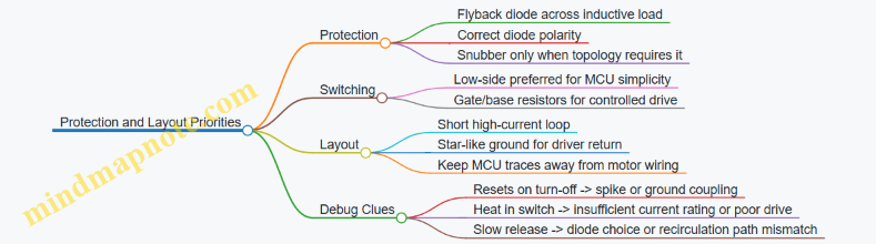
Quick Validation Procedure
Before connecting the MCU, test the switching stage with a multimeter and a current-limited supply if available. Confirm:
- The switch turns on fully (low voltage drop across MOSFET or transistor).
- The diode is correctly oriented (no unintended conduction).
- The supply voltage does not collapse when the load turns on.
Once the hardware behaves predictably, then connect the MCU and verify that turning the load on and off does not disturb logic operation.
7.5 Validate Timing and Electrical Safety for Mixed Loads
Mixed loads means you’re driving different kinds of electrical behavior from the same system: logic-level sensors, inductive actuators, resistive heaters, and maybe a relay or two. The goal of this section is simple: prove that your timing assumptions match reality, and that your electrical design prevents unsafe states even when signals misbehave.
Start with a Timing Map That Matches the Wiring
Before measuring anything, write down the “who talks to whom” timeline. Treat each control line as a signal with a direction, a source, and a required settling time.
- Define control phases: power-up, sensor read window, actuator enable window, and power-down.
- Assign minimum delays: e.g., after enabling a regulator, wait for rails to stabilize before reading analog sensors.
- Assign maximum tolerances: e.g., actuator enable must not occur until a safety interlock input is stable.
A practical rule: if you can’t point to a specific delay requirement, you’re guessing.
Validate Timing with Measured Events, Not Just Firmware Delays
Firmware delays are guesses unless you verify them with signals.
- Pick probe points: measure the actuator control pin, the supply rail, and one representative sensor signal.
- Trigger on a known event: for example, the rising edge of a GPIO that enables the actuator driver.
- Record three intervals:
- Control-to-rail rise time
- Rail-to-sensor-valid time
- Control-to-current rise time (for inductive loads)
If your measured intervals don’t match your assumptions, fix the hardware timing (power sequencing, RC filters, driver enable logic) before rewriting firmware.
Electrical Safety for Mixed Loads Means “Fail Safe,” Not “Fail Quiet”
Safety here is about preventing harmful electrical states: unintended motor motion, latch-up, overheating, or damaged GPIOs.
- Use proper driver stages: never switch inductive loads directly from MCU GPIO.
- Add energy management: flyback diodes for inductive loads, snubbers where needed, and correct polarity for suppression parts.
- Prevent back-powering: ensure signal lines and peripherals can’t feed the MCU through protection diodes when the main rail is off.
- Limit fault current: fuses or resettable fuses for power rails, and series resistors or current-limiting strategies for sensitive signals.
Mind Map: Timing and Safety Validation Workflow
Example: Safe Sequencing for a Sensor Plus Inductive Actuator
Assume a system reads an analog sensor and then enables a solenoid. The solenoid driver has a flyback diode, and the MCU controls the driver enable pin.
Hardware expectations:
- The solenoid enable pin must not go high until the sensor rail is stable.
- The sensor read must occur before the solenoid current ramps.
Validation steps:
- Power the board and trigger on the solenoid enable GPIO rising edge.
- Measure the sensor rail voltage and the analog sensor output.
- Confirm that sensor readings occur in a window where the solenoid current is still near zero.
- Confirm that the solenoid current ramp doesn’t cause rail dips that push the MCU into brownout.
If you see rail dips, add bulk capacitance near the driver, improve ground return routing, or separate noisy returns from the sensor ground.
Example: Interlock Timing with a Safety Input
A safety interlock input might be a button, a limit switch, or a door sensor. The key is to define what “stable” means.
- Require the interlock to be stable for N milliseconds before enabling the actuator.
- Ensure the actuator disable path is immediate when the interlock changes.
Validation:
- Toggle the interlock while monitoring the actuator enable pin.
- Confirm that enable occurs only after stability is satisfied.
- Confirm that disable happens within your defined maximum response time.
Electrical Checks That Catch Real-World Problems
Do these before you trust the system:
- Back-power test: power only the actuator rail and verify the MCU rail stays at 0 V.
- GPIO stress test: drive the actuator control line through its worst-case voltage levels and confirm no unintended current flows into MCU pins.
- Thermal sanity check: run the mixed-load scenario long enough to observe regulator and driver temperatures under expected duty.
Case Study: Mixed Loads That Fail Because of Ground and Timing
A common failure pattern is “it works on the bench, then misbehaves when the actuator runs.” The usual culprits are ground bounce and timing overlap.
- Ground bounce shifts sensor readings during the solenoid ramp.
- Overlapping sensor reads with actuator enable creates inconsistent ADC results.
- A missing or weak suppression path increases current rise time variability.
Fixes are mechanical and electrical: separate returns, add local decoupling at the driver, enforce a strict state machine order, and verify with the three measured intervals described earlier.
Summary Validation Checklist
- Timing map exists and includes minimum and maximum delays.
- Measurements confirm control-to-rail, rail-to-sensor, and control-to-current intervals.
- Inductive energy is suppressed correctly and polarity is verified.
- Back-powering is prevented across power-off states.
- Interlock stability and disable response times are proven with probes.
- Mixed-load operation is checked for rail stability and thermal limits.
8. Prototyping to Production Readiness for IoT Hardware
8.1 Convert Breadboard Wiring into Schematic and Layout Plans
Breadboards are great for learning and fast iteration, but they hide two things you must make explicit for production: electrical intent and physical connectivity. The goal of this section is to turn a working breadboard into (1) a schematic that states what connects to what, and (2) a layout plan that states where those connections go and how they behave electrically.
Start with a Wiring Inventory
Before drawing anything, capture what you built. Create a simple list with one row per breadboard connection: source pin, destination pin, signal name, and expected behavior. If you used jumpers, note their function (power rail, I2C SDA, SPI MOSI, interrupt line, etc.). This inventory prevents the classic mistake of “schematic says one thing, wiring does another.”
A practical rule: every wire on the breadboard should become either a named net in the schematic or a deliberate power/ground connection. If a wire has no name, it probably should not survive the transition.
Name Nets So the Schematic Tells the Truth
On a breadboard, “5V” and “GND” are obvious. Everything else needs names. Use consistent net names across Arduino and ESP32 projects, such as SDA, SCL, MOSI, MISO, SCK, CS, INT, EN, TXD, RXD, and PWM_OUT. For analog signals, include the ADC channel in the name, like ADC_TEMP.
When you name nets, you also decide what they mean electrically. For example, SDA implies open-drain behavior with pull-ups; INT implies an input with a defined edge and pull strategy.
Translate Components into Schematic Symbols
Map each breadboard part to a schematic symbol with the right electrical type. A resistor is a resistor; a regulator is a regulator; a transistor is a transistor with pins that match your wiring. Pay attention to pin order and package differences—breadboard labels are often forgiving, schematics are not.
For power parts, include the regulator input and output nets explicitly. For decoupling capacitors, place them in the schematic near the IC power pins, even if the breadboard spacing was “close enough.” Production layout will not forgive missing decoupling.
Convert Jumpers into Nets and Connections
Breadboard jumpers usually represent direct connections, but sometimes they hide design decisions. For example:
- If you used a jumper to “share ground,” that becomes a ground net.
- If you used a jumper to connect a sensor VCC to a rail, that becomes a power net with a defined source.
- If you used a jumper to bypass a resistor or capacitor, that becomes a deliberate omission or a different component value.
Treat each jumper as a question: “Is this a net tie, or is it a temporary workaround?” Only net ties survive.
Mind Map: From Breadboard to Schematic and Layout
Build the Schematic in Blocks, Not as One Big Drawing
A schematic becomes manageable when you draw it as blocks that match your breadboard structure. A typical IoT hardware schematic block set:
- Power input and regulation
- MCU section (Arduino/ESP32)
- Sensor/actuator interfaces
- Level shifting or buffering (if used)
- Connectors and programming/debug headers
Within each block, connect nets by name. Then connect blocks together at the net level. This approach makes it easier to spot missing pull-ups, swapped pins, or forgotten grounds.
Create a Layout Plan Before You Route
A layout plan is not the final PCB artwork; it is a placement and routing strategy. Start with placement priorities:
- Place the MCU and its power input/regulator components first.
- Place high-current drivers and their flyback/decoupling parts next.
- Place connectors and test points so they are reachable after assembly.
- Place sensors and their analog front ends with attention to separation from noisy switching nodes.
Then define routing priorities:
- Route power and ground as wide, direct paths.
- Route clock-like signals (SPI SCK, UART TX/RX) away from noisy switching traces.
- Keep analog traces short and referenced to a clean ground strategy.
Add Measurement Points and “Debug Hooks” Early
On a breadboard, you can probe anything. On a PCB, you need planned access. In your layout plan, mark test pads for:
- Regulator output
- 3.3 V and 5 V rails (as applicable)
- Reset line
- UART TX/RX (or at least one of them)
- Key sensor signals (especially analog inputs)
This is not for convenience only; it reduces the time spent guessing when a board behaves differently than the breadboard.
Example: Converting a Breadboard I2C Sensor Setup
Suppose your breadboard had an ESP32, an I2C sensor, and two pull-up resistors.
- Breadboard behavior: SDA and SCL shared across sensor and MCU, with pull-ups to 3.3 V.
- Schematic translation:
- Create nets
SDAandSCL. - Add pull-up resistors from
SDAto3V3and fromSCLto3V3. - Connect sensor pins to the nets by name.
- Ensure sensor ground ties to
GND.
- Create nets
- Layout plan:
- Place the sensor close to the ESP32 I2C pins.
- Route
SDAandSCLas a pair with minimal detours. - Keep them away from motor/relay switching traces.
- Add test pads for
SDA,SCL, and3V3.
Verification Checklist Before You Leave the Breadboard Behind
- Every breadboard wire has a net name or a documented removal.
- Power rails and ground are explicit in the schematic.
- Pull-ups, pull-downs, and enable pins are represented as components, not “mystery wiring.”
- The layout plan includes test points and defines placement order.
- You can trace any breadboard connection from inventory to schematic net to planned PCB location.
Once these steps are consistent, the transition from prototype to PCB becomes a mechanical process rather than a detective story.
8.2 Select Components With Availability and Tolerance Constraints
Component selection is where “it worked on the bench” either becomes “it ships reliably” or becomes a scavenger hunt during assembly. The goal is to choose parts that are (1) available in the quantities you need, (2) tolerant enough for your electrical and mechanical requirements, and (3) consistent enough that your production test can pass with predictable margins.
Start with a Requirements Checklist
Before picking any part numbers, write down what the component must do in measurable terms.
- Electrical constraints: voltage range, current range, switching speed, input/output thresholds, and noise sensitivity.
- Tolerance constraints: acceptable error in resistance, capacitance, gain, offset, or timing.
- Environmental constraints: operating temperature, humidity exposure, vibration, and any outdoor or enclosure limits.
- Interface constraints: package type, pin pitch, connector style, and mounting method.
A practical habit: translate each requirement into a “pass/fail” test you can run later. If you cannot imagine a test, you are probably missing a constraint.
Availability Planning That Prevents Assembly Surprises
Availability is not just “in stock.” It is also about lead time stability and whether you can buy the same part repeatedly.
- Choose alternates early: for each critical component, identify one approved substitute with compatible electrical characteristics and footprint.
- Avoid single-source traps: if a part is essential and hard to replace, treat it as a risk and plan a substitution path.
- Match order quantities to your build plan: if you need 500 units, do not design around a component that only makes sense for 10,000-unit reels.
A simple rule for production sanity: if you cannot obtain the component in the same form factor and rating from at least two suppliers, you should expect procurement friction.
Tolerance Budgeting from First Principles
Tolerance constraints should be handled like a budget, not a hope.
- Identify the dominant error contributors. For example, in a divider-based sensor input, resistor tolerance and ADC reference error often dominate.
- Combine errors appropriately. For rough engineering margins, worst-case thinking is conservative; for tighter designs, root-sum-square is common when errors are independent.
- Allocate margin for measurement and calibration. If you plan calibration, you can relax some tolerances, but you still need the system to behave predictably during calibration.
Concrete example: Suppose you need a 3.3 V divider output that must be within ±1% for a sensor reading. If the ADC reference contributes ±0.5% and the resistor pair contributes ±1% combined, your divider output may exceed the ±1% target unless you tighten resistor tolerance or calibrate.
Component Classes and Their Typical Tolerance Sensitivities
Different parts fail in different ways, so tolerance selection should be targeted.
- Resistors: tolerance affects scaling and thresholds. For pull-ups, loose tolerances are usually fine; for divider ratios and timing networks, tighter tolerances matter.
- Capacitors: capacitance tolerance and ESR affect filtering, startup behavior, and stability. If you are filtering sensor noise, capacitance tolerance changes cutoff frequency.
- Voltage regulators: output accuracy and load regulation affect brownout margins. If you rely on a regulator to keep a rail stable during transmit or motor switching, choose tighter regulation specs.
- Crystals and oscillators: frequency tolerance impacts UART baud accuracy and timing. For serial links, keep baud error within your link budget.
- Semiconductors: gain/offset tolerances in analog front ends can dominate measurement error.
Footprint and Package Compatibility Is a Hidden Constraint
A component can be electrically perfect and still be wrong for manufacturing.
- Package footprint: confirm land pattern, pin pitch, and height clearance.
- Thermal behavior: power devices need thermal pad compatibility and airflow/enclosure assumptions.
- Solderability: lead-free vs leaded processes can change wetting behavior; ensure the package is compatible with your assembly process.
Mind Map: Availability and Tolerance Constraints
Example: Selecting Resistors for an ADC Divider
You want an ADC input that maps a 0–5 V sensor range into 0–3.3 V.
- Choose resistor values to hit the ratio with headroom for ADC input limits.
- Pick resistor tolerance based on your measurement requirement. If you need ±2% overall accuracy, do not assume “±5% resistors are fine.” Budget the divider ratio error plus ADC reference error.
- Confirm resistor power dissipation at 5 V and worst-case tolerance, since tighter tolerances often come with different power ratings.
A good selection process ends with an incoming inspection plan: if the divider ratio is critical, you either test the assembled divider during production or tighten resistor tolerance enough that you can trust the ratio without per-unit measurement.
Example: Regulator Choice for Brownout Immunity
If your ESP32 board must not reset during a high-current event, regulator selection must consider both accuracy and transient behavior.
- Use the regulator’s dropout and load regulation specs to ensure the rail stays above the MCU brownout threshold.
- Add capacitance that matches the transient requirement, then verify that capacitor ESR and tolerance do not undermine stability.
- Select alternates that keep the same pinout and stability requirements, not just the same nominal output voltage.
Verification Steps That Tie Selection to Reality
After selecting parts, lock the decision with a small set of checks.
- Incoming inspection: verify critical parts by value or key parameters when tolerances matter.
- Assembly test: measure the assembled divider output or rail stability under representative load.
- Revision control: record the exact part numbers and tolerance grades used so failures can be traced without guesswork.
When availability and tolerance constraints are handled together, your hardware becomes easier to build, easier to test, and less likely to surprise you at the worst possible moment.
8.3 Design for Manufacturability with Footprints and Test Points
Manufacturability starts with footprints that match how parts are actually made and assembled, and it continues with test points that make verification practical. If you design for “it should work,” you’ll spend your time proving it. If you design for “it can be checked,” you’ll spend your time fixing only the real problems.
Footprints That Match Reality
Choose the Correct Package Variant
A footprint is not just the outline. It must match the package body, pin pitch, pin length, solder mask openings, and courtyard. For example, two “SOIC-8” parts can differ in lead span and body width. Use the manufacturer’s mechanical drawing, not the generic symbol.
Example: You place an 8-pin IC with 1.27 mm pitch but the footprint uses 1.00 mm. The board may assemble anyway, but the pins will bridge or sit off-center, and your first power-up will look like a mystery novel.
Define Land Patterns for Soldering Behavior
For through-hole and fine-pitch SMT, land patterns affect solder wetting and alignment. Keep these rules consistent across the design:
- Use solder mask expansion and paste mask openings that match your assembly process.
- Ensure pad sizes are large enough for the stencil, but not so large that they cause shorts.
- Set courtyard to cover component placement tolerances.
Add Fiducials and Keep Clearances Honest
Pick-and-place machines need fiducials for alignment. Place them where they won’t be covered by tall components. Also keep clearances between pads and nearby copper so solder paste doesn’t wick into unintended areas.
Test Points That Make Debugging Efficient
Decide What You Need to Measure
Test points should answer specific questions: “Is power present?”, “Is the regulator stable under load?”, “Is the interface alive?”, and “Is reset behaving?”. If you don’t define the question, you’ll add random pads and still not know what to probe.
Example: For an ESP32 board, you often need to measure 3.3 V at the module supply pins, not just at the regulator output. Voltage drop across traces can hide brownout issues.
Use the Right Test Point Type
Common options:
- Pad test points: Simple and cheap; good for multimeter probing.
- Via test points: Useful when you want to probe a net without adding extra surface area.
- Header or pogo pads: Best for repeatable fixture-based testing.
Pick based on how you will test. A production fixture wants repeatability; a bench workflow wants accessibility.
Place Test Points Where They Matter Electrically
A test point should be electrically close to the node you care about. For power, that means near the load. For signals, it means after any level shifting or buffering that changes the waveform.
Example: If you test a UART signal before a level shifter, you might see clean logic but still fail at the receiving device due to edge distortion or wrong voltage levels.
Label Nets and Keep Probing Unambiguous
Silkscreen labels help humans. Net names in the schematic help tools. Together they reduce the “which pad is which?” tax.
Integrated Manufacturing Checklist
Footprint Verification Steps
- Confirm package drawing matches the exact part number.
- Check pad pitch, pad shape, and solder mask/paste settings.
- Validate courtyard and keep-out rules.
- Run DRC for clearance and check for accidental copper overlaps.
Test Point Verification Steps
- Map each test point to a measurement goal.
- Ensure test points are reachable without disassembling the board.
- Confirm test points are on the correct side of level shifters and regulators.
- Verify that test points do not create shorts during assembly.
Mind Map: Footprints and Test Points
Example: Power Rail Footprint and Test Point Pairing
Suppose your design uses a 5 V input, a buck regulator to 3.3 V, and an LDO for a sensor rail.
- Footprint pairing: Use the regulator’s recommended land pattern so the thermal pad soldering behaves predictably. If the thermal pad is undersized, you may get intermittent regulation under load.
- Test point placement: Add a test point for 3.3 V near the module supply pins, and another for the sensor rail near the sensor connector. During bring-up, you can quickly distinguish “regulator output is fine” from “voltage drops on the way to the load.”
Example: Signal Test Points for Interfaces
For I2C, you want to see both the waveform and the pull-up behavior.
- Place test points on SDA and SCL close to the device connector.
- Ensure the test points are not behind series resistors unless that’s exactly what you want to observe.
For SPI, you want clean edges and correct chip-select timing.
- Add a test point for SCLK and CS near the target device.
- If you use level shifting, place the test points after the shifter so you measure what the device actually receives.
Practical Rule Set
- Footprints must match the exact part drawing.
- Test points must map to a measurement question.
- Place power test points near loads, and signal test points after any logic that changes the waveform.
- Label nets so the board is debuggable by a human with a multimeter and a deadline.
8.4 Plan Assembly and Programming Steps for Production Runs
Production runs fail in predictable ways: parts get assembled in the wrong order, firmware doesn’t match the hardware revision, and test steps are skipped because “it worked on the bench.” This section turns those failure modes into a concrete, repeatable plan.
Assembly Flow from First Solder to Final Label
Start with a build flow that mirrors how you test. If your test fixture checks power rails first, your assembly should make power rails easy to access and verify.
- Incoming inspection and kitting: Verify BOM line items, package types, and polarity-sensitive parts (diodes, electrolytics, LEDs). Create a kitting checklist that matches your BOM order, not your schematic order.
- Subassembly staging: Build the device in stages that align with test points. For example, assemble the power section first, then the MCU section, then the sensor/actuator section.
- ESD and handling rules: Define who can touch RF pins, antenna areas, and exposed connectors. A simple rule like “wear a wrist strap when handling the module” is more useful than a long policy.
- Soldering and rework discipline: Record rework events. If you remove and resolder a connector, treat it as a new inspection trigger.
- Final assembly and enclosure: Confirm that cable lengths and strain relief are correct before closing the case. Once the enclosure is on, you lose access to the most common troubleshooting points.
Programming Flow That Matches Hardware Reality
Programming is not just “flash and go.” Production programming must account for boot pins, serial wiring, and version tracking.
- Define the programming identity: Decide what uniquely identifies a unit: hardware revision, firmware version, and optionally a serial number.
- Set up a deterministic programming order: Program the MCU first, then any secondary controllers, then configuration data stored in nonvolatile memory.
- Use a single source of truth for firmware: Each firmware build should embed the hardware revision it supports. During programming, the tool should refuse mismatched combinations.
- Verify boot behavior immediately: After flashing, check that the device reaches a known “ready” state within a fixed time window.
- Lock configuration only after tests: If you store calibration constants or network settings, write them after functional tests pass, not before.
Test Points and Acceptance Criteria
A production plan needs measurable gates. Define pass/fail criteria for each stage.
- Stage A: Power verification: Measure input voltage range, regulator output, and ripple under a load step.
- Stage B: Interface verification: Confirm I2C/SPI pullups, UART TX/RX continuity, and GPIO direction assumptions.
- Stage C: Functional verification: Validate sensor readings against expected ranges and actuator control signals without exceeding safe limits.
- Stage D: System verification: Confirm boot logs, watchdog behavior, and stable operation for a fixed duration.
Mind Map: Production Assembly and Programming Steps
Example: Production Checklist for a Single Unit
Use a checklist that operators can complete without interpreting your mind.
- Before assembly: BOM revision matches work order; correct connector footprint; polarity parts verified.
- After subassembly A: Power rail voltages within tolerance; regulator temperature rise within limit.
- After MCU programming: Device enters ready state; UART console shows expected boot marker.
- After full assembly: Sensor values within calibrated range; actuator command toggles correctly; no unexpected resets.
- Final: Label includes serial number, hardware revision, and firmware version.
Example: Programming Tool Guardrails
Guardrails prevent the most expensive mistake: flashing the wrong firmware.
If hardware_revision != firmware_supported_revision:
  Abort programming
  Mark unit as HOLD
  Require engineering review
Else:
  Flash firmware
  Wait for ready marker
  If ready marker not seen:
    Retry once
    If still failing:
      HOLD and log UART output
Documentation and Traceability That Actually Gets Used
Traceability should be lightweight but complete.
- Per-unit record: Store serial number, hardware revision, firmware version, and test results for each stage.
- Per-lot record: Track component lot numbers for critical parts like regulators, flash memory modules, and connectors.
- Nonconformance handling: Define what “HOLD” means, who clears it, and what evidence is required.
Example: Traceability Template for Test Records
Unit Serial: ________
Hardware Revision: ________
Firmware Version: ________
Stage a Power: PASS / FAIL (notes: ________)
Stage B Interfaces: PASS / FAIL (notes: ________)
Stage C Functional: PASS / FAIL (notes: ________)
Stage D System: PASS / FAIL (duration: ________)
Operator: ________  Date: 2026-02-20
Practical Sequencing Rules That Reduce Rework
- Program before you close the enclosure so you can still access UART and power test points.
- Test after each assembly stage so failures are localized.
- Never reuse a “known good” firmware build across hardware revisions without an explicit compatibility check.
A production run is a chain of small, verifiable steps. When each step produces a measurable outcome and updates the unit’s record, the process becomes calm—even when something goes wrong.
8.5 Create Hardware Acceptance Tests for Each Build
Hardware acceptance tests answer one question: “Does this exact build behave correctly under defined conditions?” The trick is to test what can fail without needing a full product simulation. Start with a baseline checklist, then add targeted tests that map directly to your schematics, firmware expectations, and assembly steps.
Acceptance Test Strategy That Matches Reality
- Define build identity and scope. Record hardware revision, PCB revision, BOM variant, firmware version, and programming method. If you run tests without identity, you’ll eventually “discover” that nothing is reproducible.
- Set test conditions. Specify supply voltage range, ambient temperature, and any required peripherals. For example, if your regulator is rated for 3.3 V ±5%, test at the low end (3.135 V) and nominal (3.3 V).
- Choose pass criteria that are measurable. Prefer thresholds like “UART prints boot banner within 2 seconds” over vague statements like “seems stable.”
- Use a layered approach. Run quick electrical checks first, then functional tests, then stress tests that target known risk areas (power switching, RF transmit, high-current drivers).
Mind Map: Hardware Acceptance Test Flow
Preflight Electrical Checks
These tests catch the “oops” failures that waste hours later.
- Visual and mechanical inspection. Verify connector orientation, polarity marks, and that no solder bridges exist near power pins and MCU pins.
- Continuity and shorts. Measure resistance between adjacent power rails and between rails and ground. A near-zero reading where you expect isolation is an immediate fail.
- Power rail presence. Power the board and confirm each expected rail reaches its target voltage. Then apply a representative load (for example, a 100 mA dummy load on 3.3 V) and re-check regulation.
Example: If your design uses a 5 V input to a 3.3 V regulator, record 3.3 V at no load and at load. If the voltage droops below your firmware’s brownout threshold, you’ll see random boot failures that look like software bugs.
Interface Bring Up Tests
Acceptance tests should confirm that the hardware matches the firmware’s assumptions.
- UART boot log timing. Power-cycle the board and measure time to first UART output. Set a window, such as “within 2 seconds at nominal voltage.”
- I2C scan and addressing. Run an I2C scan and confirm expected device addresses respond. Also verify that SDA/SCL lines are not stuck low.
- SPI link sanity. If you have a known SPI device, read a fixed register value. If you don’t, use a loopback test by wiring MOSI to MISO through a resistor and verifying data integrity.
- GPIO pull and direction. With firmware configured for inputs, confirm pull-ups/pull-downs produce stable logic levels. Then switch to outputs and verify the expected voltage levels with a multimeter.
Example: For an I2C sensor, don’t just check that it responds—read one calibration register and confirm it’s within a plausible range. That catches wiring errors where the bus is alive but the wrong device is connected.
Functional Verification with Safe Defaults
Functional tests should avoid stressing hardware while still proving correctness.
- Sensor readout sanity. Read each sensor at least once and check for “not-a-number” conditions like all zeros, saturated ADC values, or impossible temperature readings.
- Actuator safe state. Before enabling outputs, confirm driver pins are in the inactive state. Then enable for a short, controlled duration and verify current draw stays within your expected envelope.
Example: If a relay coil is driven through a transistor, measure coil-side voltage during activation. If it never reaches the coil voltage, you’ll get intermittent behavior that only appears in the field.
Stress and Fault Handling Tests
These tests target the failure modes you already know are risky.
- Brownout behavior. Drop supply voltage slowly or step it down to the regulator’s low operating limit and confirm the system resets cleanly rather than hanging.
- Power switching transients. If you switch motors or solenoids, verify that the MCU supply doesn’t dip below the reset threshold during switching. Use a scope if available; otherwise, log reset counts and UART continuity.
- RF transmit stability for ESP32 builds. During a transmit test, monitor supply voltage and confirm it remains within tolerance. If voltage sags, you’ll see resets or corrupted logs.
Evidence and Signoff That Engineers Can Trust
For each unit, store:
- Test date (use your internal standard; for example, 2026-02-20)
- Build identity fields
- Pass/fail per test step
- Measured values for power rails and key interfaces
- Photos or notes for any anomaly
Example: If a unit fails the I2C scan, record the exact addresses found and whether SDA/SCL were stuck. That turns a vague failure into a specific wiring or pull-up issue.
Minimal Acceptance Test Template
Use a consistent checklist so results are comparable across builds.

A good acceptance test suite is boring in the best way: it produces the same verdict for the same build under the same conditions, and when it fails, it tells you where to look.
9. PCB Design for Arduino and ESP32 Systems
9.1 Create a Practical PCB Stackup and Ground Strategy
A practical PCB stackup is mostly about two things: controlling return paths and keeping power stable where the circuit needs it. For Arduino and ESP32 hardware, you also have to respect the fact that RF transmit currents and fast digital edges both want clean ground, and they do not politely wait their turn.
Start with Your Signals and Current Paths
Begin by listing what crosses the board and how fast it is.
- Power rails: regulator outputs, battery input, and any high-current loads.
- High-speed digital: SPI, I2C (usually slower but still sensitive to bus integrity), UART, and any fast GPIO driving.
- RF: ESP32 antenna feed and any RF-adjacent traces.
- Analog: ADC inputs, sensor excitation, and reference networks.
Then decide where current should flow. In general, the return current follows the path under the signal trace. If you route a signal over a split or poorly connected ground, the return current detours, and your measurements start behaving like they are haunted.
Choose a Stackup That Matches Your Board Complexity
A common, workable baseline for mixed Arduino/ESP32 boards is a 4-layer stackup:
- Top layer: signals and some power routing.
- Layer 2: solid ground plane.
- Layer 3: power plane(s) or split power with careful stitching.
- Bottom layer: remaining signals.
If you must use 2-layer, you can still succeed, but you need more discipline: wider ground pours, careful routing to avoid long gaps, and more attention to where you place return paths.
Ground Plane Strategy That Actually Works
A ground strategy is not just “make a plane.” It is about how the plane is segmented, stitched, and referenced.
Single Solid Ground Reference
For most designs, keep a continuous ground plane under the digital and RF regions. This reduces loop area and makes return paths predictable.
Split Planes Only When You Have a Reason
Splitting ground can help isolate noisy sections, but it also creates impedance discontinuities. If you split, you must define where the grounds connect and how signals cross the boundary.
A safe default is:
- Keep one continuous ground plane.
- Use separate power routing and component placement to manage noise.
- If you need separation for analog, isolate at the power and routing level, not by cutting the ground plane.
Power Plane and Decoupling Placement Rules
Power stability is a layout job, not a component job.
- Decouple at the pins: place 0.1 µF (and often a bulk capacitor) as close as possible to each IC power pin.
- Use via pairs: connect each decoupling capacitor to the relevant planes with short, direct vias.
- Avoid routing signal traces between a device and its decoupling capacitor.
- Keep high-current return paths out of sensitive analog ground areas.
For ESP32, pay special attention to the power path feeding the module. RF transmit current causes voltage droop if the plane connection is narrow or indirect.
Via Stitching and Boundary Control
Use via stitching to reduce impedance across the board.
- Stitch ground around board edges and around large plane transitions.
- Stitch frequently near connectors, mounting holes, and areas where you change layer usage.
- For any ground split you cannot avoid, stitch across the boundary at a controlled location.
Mind Map: Stackup and Ground Decisions
Example: A Typical 4-Layer Stackup for ESP32
Use this as a starting point, then adjust to your board thickness and fabrication constraints.
- Layer 1 (Top): signals, short power traces, keep-out under antenna area.
- Layer 2 (GND): uninterrupted ground plane.
- Layer 3 (PWR): 3.3 V and other rails as planes or pours with controlled segmentation.
- Layer 4 (Bottom): remaining signals.
Place decoupling capacitors for the ESP32 and any fast digital ICs on the top layer, directly adjacent to their power pins, with vias that drop straight into the ground and power planes.
Example: Ground Split Mistake to Avoid
If you cut the ground plane to “separate analog,” but route a digital trace across the cut, the return current will detour around the split. The analog reference then sees the detour current through parasitic coupling, and your ADC readings will show patterns that match the digital activity.
A better approach is to keep the ground plane continuous and instead:
- route analog traces away from high-edge-rate signals,
- filter and reference analog inputs locally,
- keep high-current returns away from the analog front end.
Quick Checklist Before You Send Gerbers
- Ground plane is continuous under RF and digital regions.
- Decoupling is placed at IC pins with short via connections.
- Power entry to ESP32 has a low-impedance path into the planes.
- No signal crosses a ground discontinuity without a defined return strategy.
- Via stitching covers edges, connectors, and any unavoidable segmentation boundaries.
9.2 Route High Current Paths and Separate Noisy Returns
High current routing is mostly about controlling where voltage drops happen. When current flows through copper, it creates a small but real voltage difference across that copper. If a “noisy” return shares the same path as a “quiet” return, the quiet signals inherit that voltage difference as error.
Foundational Rule Set
Start with three practical rules:
- Keep forward and return paths close together. A tight loop reduces the area that can pick up or radiate noise.
- Route high current on dedicated copper. Use wider traces or pours for the power path, and keep them away from sensitive analog and logic.
- Separate returns by function, then join at a single point. “Single point” means one intentional connection between noisy and quiet grounds, usually at the power entry or regulator output.
A quick mental model: treat each current loop like a small antenna. Smaller loop area means less coupling.
Identify Which Currents Are “High” and Which Returns Are “Quiet”
On Arduino and ESP32 boards, high current often comes from motor drivers, solenoids, LEDs, heater elements, and sometimes USB-to-5 V rails feeding multiple loads. Quiet returns include sensor grounds, ADC reference returns, and the MCU ground reference for measurement.
Before routing, label nets in your schematic:
- Power nets: motor supply, relay coil supply, LED strip supply.
- Switching nodes: MOSFET drain/source nodes, relay driver outputs.
- Sensing nets: sensor ground, analog ground, reference ground.
Then mirror those labels on the PCB so you can route with intent rather than hope.
Layout Strategy from Power Entry to Load
- Start at the power entry. Place the bulk capacitor close to where power enters the board. This capacitor absorbs fast current changes locally.
- Create a power spine. Route the main supply as a wide trace or polygon. Keep it short and direct.
- Route noisy loops locally. For each switching load, keep the loop area small: supply → switch → load → return.
- Use a star-like join for grounds. Connect noisy return and quiet ground at one controlled location, typically near the regulator or power connector.
- Keep sensitive traces away from switching copper. Maintain spacing from MOSFET gate/drain copper and from high-current return pours.
Practical Example: MOSFET-Driven Solenoid
Suppose you drive a solenoid from 12 V using a logic-level MOSFET.
- Route 12 V to the solenoid and MOSFET using a wide trace.
- Route the solenoid return back to the MOSFET source or driver ground node using a dedicated wide path.
- Place the flyback diode physically close to the solenoid terminals and MOSFET so the high di/dt loop stays compact.
- Connect that noisy return to the main ground at the single join point, then route sensor ground separately to the MCU.
If you instead run the solenoid return through the same ground pour as the sensor ground, the ADC can “see” the solenoid current steps as offsets.
Advanced Details That Matter
- Avoid splitting a ground pour unintentionally. If you separate grounds, do it intentionally with a controlled join. Accidental splits can create long return paths.
- Control where current crosses layers. Via placement affects loop geometry. Prefer vias that keep the loop tight rather than vias that “shortcut” across sensitive areas.
- Use Kelvin-style sensing for current sense or ADC references. If you measure a voltage drop across a resistor, route the sense lines separately from the high-current pads.
- Don’t route signal returns under high-current traces. Even if the net name is the same, the physical path matters.
Mind Map: High Current Routing and Noisy Returns
Quick Checklist Before You Send Gerbers
- High current traces are wider than signal traces.
- Switching loops are compact and do not wander across the board.
- Noisy return does not share the same copper region with sensor ground except at the planned join.
- Bulk capacitance is near the power entry and near the switching supply node as appropriate.
- Any sense lines are routed separately from the high-current copper.
When these conditions are met, the board stops “mysteriously” resetting or misreading sensors when actuators turn on. The fix is usually not firmware; it’s copper behaving like copper.
9.3 Place Decoupling Capacitors and Control Impedance Where Required
Decoupling capacitors are not “extra parts”; they are the local energy buffer that keeps voltage rails from wobbling when current changes quickly. On Arduino and ESP32 boards, the wobble usually shows up as random resets, I2C glitches, ADC noise, or RF-related brownouts. The goal is simple: make the path from the capacitor to the load electrically short, so the capacitor can respond before the regulator and bulk capacitors “feel” the demand.
Foundational Idea: Impedance Beats Capacitance
A capacitor’s effectiveness depends on the impedance of the entire loop: capacitor → via → plane → return path → back to the source. Even a large capacitor can be slow if the loop inductance is high. Placement reduces loop area, which reduces inductance, which reduces impedance at the frequencies where current steps occur.
Where to Place Capacitors
Use a three-tier approach.
- Bulk capacitors near the power entry or regulator output handle slower changes and larger energy needs.
- Decoupling capacitors near each power-consuming IC handle fast current steps.
- Local capacitors near sensitive analog nodes or RF sections handle very fast, localized disturbances.
For decoupling, the rule is: place the capacitor so that the capacitor’s terminals connect directly to the same power and ground planes the IC uses, with minimal via count.
Control Impedance: Treat Power Like a Transmission Line
Control impedance means managing how current returns. High-speed edges (GPIO switching, SPI clocks, ESP32 RF bursts) create voltage drops where return paths are forced to detour. You control this by:
- Keeping a continuous ground plane under the signal routing.
- Using short, direct returns for each high-current device.
- Avoiding “split personality” grounds that make return currents wander.
When you must cross a gap or route over a cut, expect extra inductance and more rail noise.
Practical Placement Workflow
- Identify current-step sources: MCU core supply, radio section, motor drivers, buck converters, and any IC with fast edges.
- Pick the rail each device actually uses (3.3 V, 5 V, analog rail, RF rail).
- Place decoupling at the device pins: aim for the shortest loop from capacitor to the IC power pin and back to the IC ground pin.
- Use multiple values: a common pattern is one small-value capacitor for high-frequency response and one larger-value capacitor for mid-frequency response.
- Verify with measurement points: if you can, probe the rail at the IC supply pin and at the regulator output to see how much the rail droops locally.
Mind Map: Decoupling Placement and Impedance Control
Example: ESP32 Decoupling Around a 3.3 V Rail
Suppose your ESP32 module is powered from a 3.3 V regulator. Place a bulk capacitor near the regulator output, then add decoupling capacitors close to the ESP32 power pins. If your design also includes an external sensor on the same 3.3 V rail, add a separate decoupling set near the sensor IC rather than relying on the ESP32’s capacitors.
A common mistake is placing all decoupling near the regulator “because it’s convenient.” That increases loop inductance between the capacitor and the ESP32 pins, so the ESP32 sees a droop during RF transmit bursts.
Example: Arduino-Style Mixed Digital and Analog
If you have an ADC input that measures a slow analog signal, the ADC still rides on a digital 5 V or 3.3 V rail. Place decoupling capacitors near the ADC reference and analog supply pins (or near the analog front-end IC), and keep the analog return path tied to the main ground plane at a controlled point. The point is not to isolate grounds completely; it’s to prevent the analog return from sharing the same narrow, noisy return segment as motor or relay currents.
Example: Control Impedance with Routing Discipline
If you route SPI lines from the MCU to a peripheral while the ground return is forced to travel around a split plane, you create a larger effective loop for each edge. Fix it by routing the SPI traces over the ground plane and ensuring the return path is directly underneath. If you must use a via fence, do it near the transition areas so the return current has a predictable path.
Quick Checklist for the Layout
- Decoupling capacitors are within a few millimeters of the IC power pins.
- Capacitor ground connects to the same ground plane the IC uses, with minimal vias.
- High-current devices have their own local decoupling.
- Analog front-ends have local decoupling and clean return routing.
- No “all capacitors at the regulator” layout.
When these rules are followed, the rail becomes locally stiff, and the rest of your bring-up work gets easier because the hardware stops changing its mind every time a pin toggles.
9.4 Design Antenna and RF Layout Constraints for ESP32
ESP32 boards usually fail in predictable ways: the antenna feed gets noisy, the ground reference is sloppy, or the RF trace behaves like a random wire. This section focuses on the layout constraints that keep the antenna match stable and the RF path repeatable.
Core Antenna Choices and What They Imply
Start by identifying the antenna type your module expects. Many ESP32 modules use either an onboard PCB antenna or an external antenna connector. PCB antennas are sensitive to nearby copper and board edges; external antennas are sensitive to feed impedance and connector placement. In both cases, treat the RF section as a controlled system: defined geometry, defined ground, defined keepouts.
RF Stackup and Ground Reference
A stable ground plane is the quiet hero of RF layout. Use a continuous ground plane under the RF feed and antenna region, and avoid splitting it with signals. If you must route other traces near the antenna, route them on the opposite side and keep them away from the RF keepout.
Practical constraints:
- Use the same layer stackup as the module reference design when possible.
- Keep the RF feed trace referenced to ground with minimal discontinuities.
- Avoid vias in the middle of the RF feed unless the reference design uses them.
Controlled Impedance for the Antenna Feed
The RF feed trace is not “just a trace.” Its width, thickness, and distance to ground determine the characteristic impedance and the effective match at the antenna port. If the feed impedance drifts, the radio may still transmit, but the power transfer and receiver sensitivity degrade.
Layout actions:
- Use the PCB vendor’s impedance calculator for your stackup.
- Match the feed geometry to the module’s antenna port requirements.
- Keep the feed length consistent with the reference design; longer traces add loss and phase shift.
Keepouts and Copper Proximity Rules
PCB antennas dislike nearby copper because it changes the antenna’s effective capacitance and current distribution. Define keepout zones around the antenna area and the feed transition. Also watch for solder mask and silkscreen: they can slightly alter the effective geometry, especially at the antenna edge.
Concrete approach:
- Create a polygon keepout around the antenna and the immediate feed region.
- Place no copper, no vias, and no components in the keepout unless the reference design explicitly allows it.
- Route digital traces so they do not cross the keepout; if you must cross, do it far away and on a different layer.
Feed Transition and Matching Network Placement
Most ESP32 antenna feeds include a matching network or rely on module-integrated matching. Either way, the placement matters. Put matching components close to the antenna port and keep the connections short and direct.
Rules of thumb that hold up in real boards:
- Place the matching components adjacent to the RF port, not near the MCU.
- Keep the RF trace from the port to the first matching element as short as possible.
- Avoid routing other nets between the RF port and the matching network.
Via Strategy and Ground Stitching
Vias are useful for grounding, but they can also create inductance and disrupt the RF return path. Use via stitching to maintain a low-impedance ground plane around the RF region, especially near the antenna feed and any ground reference boundaries.
Guidelines:
- Stitch ground around the antenna keepout boundary.
- Prefer multiple small vias over a single large via for ground continuity.
- Keep via placement consistent with the reference design when available.
Antenna Edge, Board Outline, and Enclosure Effects
The board edge changes the antenna’s boundary conditions. If your antenna is near the board edge, the cutout and the distance to the edge can shift the resonance. Enclosures and nearby metal can also detune the antenna.
Layout checks:
- Respect the antenna-to-edge distances from the module documentation.
- Keep internal metal planes and mounting hardware away from the antenna region.
- If there is a shield can, ensure it does not overlap the antenna keepout.
Measurement Mindset and Layout Verification
Even a “correct” layout can be wrong for your exact stackup. Verify with RF-aware checks: continuity of the ground plane, absence of unintended copper in keepouts, and controlled impedance for the feed. If you have access to an RF test setup, measure return loss or at least confirm transmit power stability across supply variations.
Mind Map: ESP32 Antenna and RF Layout Constraints
Example: A PCB Antenna Layout That Stays Put
Imagine a two-layer board with a PCB antenna on the top side. You place the antenna at the edge, then route a digital trace on the same layer near it “just for convenience.” The antenna resonance shifts, and the match becomes inconsistent across builds because the copper area varies with routing.
A better layout:
- Put the digital trace on the bottom layer.
- Create a copper keepout polygon around the antenna and feed.
- Stitch ground vias around the keepout boundary at a consistent pitch.
- Route the RF feed as a controlled-impedance trace from the module port to the matching components, with no intermediate detours.
Example: External Antenna Connector Feed
With an external antenna connector, the antenna itself may be fine, but the feed can still ruin the match. A common mistake is using a random-width trace from the module to the connector.
A better approach:
- Define the feed trace impedance using your stackup.
- Keep the feed length short and direct.
- Place the matching components close to the RF port.
- Maintain a solid ground reference under the feed and stitch ground near the connector footprint.
9.5 Prepare Gerbers and Verify Design Rules Before Fabrication
Gerbers are the manufacturing “photographs” of your PCB layers. Before you generate them, you want to be confident that the board you’re about to fabricate matches the electrical intent you tested on the bench. The goal of this section is simple: produce correct files, then verify them with a repeatable checklist so surprises show up before money does.
Lock the Design State Before Exports
Start by freezing the schematic-to-layout state. Confirm that the PCB file is the one you actually want to build, and that footprints, net labels, and component values match the latest revision.
A practical workflow:
- Ensure all designators and values are final (not “DNP” placeholders unless you truly plan to omit them).
- Verify that every ERC/DRC-critical item is resolved or intentionally suppressed with a clear reason.
- Check that the board outline and keepouts are correct, because fabrication houses will treat them as law.
Example: If you changed a connector from 1x8 to 1x10 but only updated the schematic, the layout may still use the old footprint. The board will assemble, but the cable won’t.
Run Design Rule Checks with Intent
Design rule checks (DRC) catch violations like trace too close to copper pour, missing clearance, or wrong drill sizes. Run DRC in layers and categories, not as a single “all green” moment.
Use a staged approach:
- Electrical clearances: spacing between nets, annular ring sizes, and solder mask openings.
- Manufacturing constraints: minimum trace width, minimum annular ring, drill-to-copper clearance.
- Assembly-related rules: courtyard overlaps, silkscreen legibility, and forbidden layers for copper.
Example: A 0.2 mm clearance rule might pass in simulation, but if your fab’s capability is 0.15 mm and your board uses 0.16 mm in one corner, you’ll get a board that looks fine until you try to solder it.
Verify Layer Stack and Copper Assignments
Before exporting, confirm that each layer contains what you think it contains.
- Copper layers: signal, plane, and any special layers like impedance-controlled traces.
- Mask and paste: ensure openings align with pads and that you didn’t accidentally invert polarity.
- Silkscreen: check that text doesn’t overlap pads or violate minimum stroke rules.
A quick sanity check is to view the board in “layer-by-layer” mode and look for obvious mismatches: copper on the wrong side, missing pours, or mask openings that cover pads.
Generate Gerbers and Drill Files Correctly
Most fabrication errors come from file generation settings, not from the PCB itself.
Checklist for exports:
- Select the correct board layers and ensure each is mapped to the right Gerber type.
- Confirm units (mm vs mil) and coordinate origin.
- Export drill files (Excellon) with plated and non-plated holes correctly identified.
- Include solder mask and paste layers only if your fab expects them.
Example: If your drill file is exported in mil while your board is in mm, the holes will be off by a factor of 25.4. The board will still “manufacture,” but it won’t assemble.
Inspect Outputs with a Viewer Like a Detective
Open the Gerbers in a viewer and compare them to the PCB.
- Overlay check: confirm that copper, mask, and silkscreen align.
- Hole check: verify drill locations against pad centers.
- Polarity check: ensure solder mask openings are where pads are.
Look for these common issues:
- Missing or incomplete pours due to net assignment or keepout settings.
- Silkscreen cutouts that hide critical reference designators.
- Traces that appear disconnected because of a wrong layer export.
Validate Against Fabrication Capabilities
Your PCB rules should match the manufacturer’s minimums. Even if your DRC passes, you can still exceed fab constraints.
Key parameters to verify:
- Minimum trace width and spacing.
- Minimum annular ring and drill sizes.
- Solder mask expansion and minimum mask sliver.
- Copper thickness assumptions and any impedance constraints.
Example: If you used a 0.25 mm annular ring but the fab requires 0.20 mm minimum, you’re safe. If you used 0.15 mm, you’ll likely get reduced rings or solderability problems.
Produce a Build Package with Clear Naming
A fabrication package should be unambiguous.
- Use consistent revision naming across Gerbers, drill files, and any assembly drawings.
- Include a README inside the archive describing which files correspond to which layers.
- Confirm that the board outline is present and correct.
Example: A Practical Pre-Fab Checklist
Use this as a final pass before uploading files:
- DRC: no unresolved errors in clearance, annular ring, and courtyard categories.
- Layer view: copper, mask, and silkscreen align on both sides.
- Gerbers: correct layer mapping and units.
- Drill: plated/non-plated holes exported and match pad sizes.
- Viewer: overlay check shows no missing copper islands or shifted holes.
- Fab match: trace/space, ring, and drill sizes meet the manufacturer minimums.
If you follow the checklist in order, you’ll catch the two biggest failure modes: mismatched export settings and rule mismatches with fabrication capability. Both are boring, both are common, and both are preventable.
10. Firmware Hardware Coupling for Startup Reliability
10.1 Align Firmware Pin Maps With Hardware Schematics
Pin alignment is where “it compiles” meets “it works.” The goal is simple: every firmware pin name must point to the exact net and electrical role shown on the schematic, with no silent assumptions about board variants, boot straps, or connector numbering.
Foundational Workflow
Start with a single source of truth for each layer:
- Schematic nets define what connects to what.
- PCB pin numbers define physical pads.
- Firmware pin maps define which MCU GPIO is used.
Your job is to connect these three layers with evidence, not memory.
Step 1: Create a Pin Role Inventory
Write down each signal with its role, not just its name. For example:
SENSOR_SDA: I2C data line, open-drain with pull-up.SENSOR_SCL: I2C clock line.MOTOR_EN: logic input to a driver.STATUS_LED: active-high or active-low.
This prevents the classic mistake of mapping a GPIO that “looks right” but has the wrong electrical behavior.
Step 2: Map MCU Pins to Schematic Nets
For each MCU pin in the schematic, record:
- MCU GPIO number (or Arduino pin label)
- Schematic net name
- Connector reference if it leaves the board
- Electrical notes (pull-up, pull-down, open-drain, level shifting)
Then mirror that mapping in firmware using the same net names as the schematic, so review is mechanical.
Step 3: Validate Against Boot and Reset Behavior
ESP32 and some Arduino-compatible boards have pins that affect boot mode. If a schematic shows a strap resistor network, the firmware must never treat that GPIO as a free general-purpose output at reset.
A practical rule: if the schematic includes any boot-related pull-up/pull-down, treat the GPIO as “reserved until proven safe,” and document the safe direction and default state.
Mind Map: Pin Alignment Chain
Integrated Example: I2C and an LED
Assume the schematic shows:
U1is the MCU.R10andR11are pull-ups onSENSOR_SDAandSENSOR_SCL.D1isSTATUS_LEDconnected through a resistor toGPIO_2.
In firmware, define pins using the schematic net names, then assign them to the MCU GPIOs:
SENSOR_SDA->GPIO_21SENSOR_SCL->GPIO_22STATUS_LED->GPIO_2(active-high if the LED anode is on the GPIO side)
If the LED is wired active-low, the firmware should invert the logic once, not scatter inversions across the codebase.
Example: Pin Map Table
| Schematic Net | Role | MCU GPIO | Firmware Symbol | Notes |
|---|---|---|---|---|
| SENSOR_SDA | I2C Data | 21 | SDA_PIN | Open-drain, pull-up present |
| SENSOR_SCL | I2C Clock | 22 | SCL_PIN | Open-drain, pull-up present |
| STATUS_LED | Indicator | 2 | LED_PIN | Verify active level |
Verification Techniques That Catch Real Mistakes
Compile-Time Guardrails
Use a single header that defines all pins. Avoid hard-coded GPIO numbers scattered across modules.
// pins.h
#Pragma Once

constexpr int SDA_PIN = 21;
constexpr int SCL_PIN = 22;
constexpr int LED_PIN = 2;

// Optional: prevent accidental reuse
static_assert(SDA_PIN != LED_PIN, "Pin collision: SDA and LED share a GPIO");
This doesn’t prove electrical correctness, but it prevents the “copy-paste swap” class of bugs.
Runtime Sanity Tests
Before running the full application, do a minimal bring-up:
- Blink the LED using the firmware symbol.
- Scan the I2C bus and confirm devices respond at expected addresses.
If the I2C scan returns nothing, the issue is often pin mapping, pull-ups, or bus speed—not the sensor.
Advanced Details Without the Guesswork
Handle Connector Numbering Separately
A connector pin label like J1-4 is not the same thing as an MCU GPIO. Keep a separate mapping layer:
- Connector pin -> schematic net
- Schematic net -> MCU GPIO
This separation makes reviews easier because a reviewer can trace from connector to net without reading firmware.
Track Revisions
If the schematic changes, the firmware pin map must change with it. Store the pin table alongside the code and note the schematic revision it matches. A mismatch is the silent killer of “works on my bench.”
Review Checklist
- Every firmware pin symbol has a matching schematic net name.
- Boot/strap pins are documented with safe usage rules.
- Active levels are correct for LEDs and enable lines.
- I2C pins are configured as open-drain with pull-ups present on the schematic.
- No GPIO numbers are duplicated across files.
- A minimal bring-up test exists for LED and I2C.
When these conditions hold, pin alignment becomes a traceable process rather than a hope-based ritual.
10.2 Implement Hardware Self Checks Using Measured Signals
Hardware self-checks are most useful when they measure the signals that matter, compare them to expected ranges, and report results in a way that points to the likely fault. The goal is not to “prove everything is perfect,” but to catch common wiring, power, and configuration issues early—before the system starts driving loads or relying on sensors.
Define What to Measure First
Start with a short checklist of signals that reveal 80% of startup problems:
- Power rails: input voltage, 3.3 V (or 5 V), and any switched rails.
- Reset and boot conditions: reset cause, strap pin states (ESP32), and clock stability indicators.
- Reference signals: ADC reference sanity (for analog sensors) and known-good digital loopback.
- Interface health: I2C/SPI bus activity and presence of expected devices.
- Load safety: outputs that must remain inactive until checks pass.
A practical rule: measure before you configure peripherals aggressively. For example, confirm rail voltage and reset cause first, then bring up I2C/SPI, then start sensor reads.
Build a Measurement Strategy That Avoids False Failures
Measured signals can be noisy at startup. Reduce false negatives by:
- Sampling multiple times: take N readings and use median or average with bounds.
- Waiting for stabilization: allow regulators to settle after enabling rails.
- Using thresholds with hysteresis: treat “slightly low” differently from “definitely wrong.”
- Checking plausibility, not perfection: for example, ADC readings should land in a reasonable window for a known divider.
Example: if you expect 3.3 V, don’t require exactly 3.300 V. Use a window like 3.15–3.45 V, and log the measured value.
Implement Self Checks with a Clear Pass/Fail Model
Use a structured result object so logs are consistent:
- Status: pass, warn, fail.
- Measured value: raw ADC counts or voltage.
- Expected range: min/max.
- Action: continue, limit behavior, or halt.
Keep the actions conservative. If power is out of range, avoid starting RF transmit, motor control, or high-current switching.
Use Measured Signals for Power and Reset
Power checks should include both “is it present” and “is it stable enough.” A simple approach:
- Read rail voltage.
- Read again after a short delay.
- Optionally sample during a small load step (e.g., enable a low-power peripheral) to detect sag.
Reset checks should record the reset cause and correlate it with power readings. If you see repeated brownouts, the measured rail will usually confirm the pattern.
Add Interface Self Checks That Confirm Wiring
For I2C, a presence check can be more informative than a single read:
- Scan expected addresses.
- For each found device, attempt a register read that should return a stable value.
For SPI, confirm chip-select discipline:
- Ensure CS is held high during idle.
- Perform a read of a known register on each expected device.
If you can spare pins, add a digital loopback test: connect one output to one input through a resistor and verify the logic level. This catches swapped pins and missing pull-ups.
Keep Outputs Safe Until Checks Pass
Treat outputs as “guilty until proven innocent.”
- Default GPIOs to inactive states at reset.
- Only enable drivers after power and interface checks pass.
- For actuators, add a software interlock that refuses to energize unless the system has passed self-checks in the current boot.
Example Self Check Flow for Startup
Boot
  -> Initialize minimal GPIO and ADC
  -> Measure rails (sample N times)
  -> Read reset cause
  -> If rail fail: log and halt or enter safe mode
  -> Enable I2C/SPI clocks
  -> Scan expected devices
  -> Validate one register per device
  -> Run analog plausibility check
  -> If all pass: enable sensor reads and outputs
  -> If warn: continue with reduced behavior
Mind Map: Hardware Self Checks Using Measured Signals
Example: Analog Plausibility Check with a Known Divider
If you can add a resistor divider from a stable reference to an ADC pin, you get a repeatable test point. At startup:
- Read ADC counts.
- Convert to voltage using the configured divider ratio.
- Compare to an expected window.
If the value is far off, you likely have a wiring issue, wrong divider ratio, or ADC reference problem. This is more reliable than assuming the sensor is present and behaving.
Example: I2C Device Presence with Register Validation
An address scan alone can mislead when a bus is stuck or a device responds but not correctly. A better pattern:
- Scan expected addresses.
- For each found device, read a register that should have a stable reset value.
- If the read fails or the value is out of range, mark warn or fail depending on criticality.
This turns “something is wrong” into “the device at address X is not responding correctly.”
Make Logs Useful Without Flooding
Log only what helps triage:
- One line per check with status and measured value.
- Include the action taken.
- Avoid printing raw samples unless a check fails.
A good log makes it possible to reproduce the fault from a single boot record, which is exactly what you want when hardware behaves differently across units.
10.3 Configure Watchdog and Brownout Handling Correctly
A watchdog and a brownout detector solve different problems, so treat them as a pair: the watchdog recovers from software that stops making progress, while brownout handling prevents the system from running code while the supply voltage is too low to behave predictably.
Core Concepts That Drive Correct Configuration
Start by defining what “failure” means in your product. For watchdogs, failure is “the firmware isn’t reaching expected checkpoints.” For brownout, failure is “the hardware is outside safe electrical conditions.” If you configure only one side, you’ll either get resets that look random (brownout ignored) or resets that look like software bugs (watchdog too aggressive).
For ESP32-class systems, brownout detection is typically tied to the power rail stability. Watchdog timers are typically split into categories such as task-level and system-level, and they are fed by firmware activity. The practical takeaway: you must ensure that your code continues to “touch” the watchdog at a rate consistent with worst-case execution time.
Mind Map: Watchdog and Brownout Responsibilities
Watchdog Configuration That Matches Real Execution
Pick a watchdog timeout based on measured worst-case behavior, not on a guess. During bring-up, instrument your firmware so you can observe the longest time between “healthy checkpoints.” For example, if you have a sensor read loop that sometimes waits for I2C completion, measure the maximum observed latency under worst-case bus conditions.
Then ensure your firmware structure supports feeding the watchdog. A common mistake is a long blocking loop that never yields. If you use an RTOS, prefer cooperative patterns: break work into chunks, yield between chunks, and keep critical sections short.
Example: chunked work with periodic watchdog feeding
// Pseudocode for a long operation broken into chunks
void processLargeBuffer() {
  const uint32_t start = millis();
  for (size_t i = 0; i < N; i += CHUNK) {
    handleChunk(i, CHUNK);
    // Ensure progress and watchdog friendliness
    if (millis() - start > 50) {
      feedWatchdog();
      start = millis();
    }
  }
}
This pattern prevents “one giant loop” behavior. The exact feed mechanism depends on your platform, but the logic is universal: guarantee periodic progress.
Brownout Handling That Prevents Nasty Electrical Edge Cases
Brownout thresholds should be set so that the MCU resets before it starts executing with marginal voltage. If your system includes a radio transmit, the supply may dip briefly. That’s why you must validate with a load-step measurement: watch the rail during the highest current event, not just during idle.
Example: correlate reset cause with power events
void setup() {
  auto cause = getResetCause();
  if (cause == RESET_CAUSE_BROWNOUT) {
    // Keep it simple: record minimal state and avoid heavy work
    markBrownoutEvent();
  }
  initPeripheralsSafely();
}
The key is to avoid doing complex initialization that might worsen instability. If brownout resets happen, your firmware should still come up deterministically and avoid writing large amounts of data immediately.
Integration Rules That Keep Debugging Honest
- Use reset cause as the first branching decision. If you see repeated resets, you need to know whether it’s watchdog or brownout.
- Set watchdog timeouts longer than your measured worst-case latency. If you set it too short, you’ll “teach” the watchdog to misdiagnose normal delays as failures.
- Keep critical sections short. If interrupts are disabled for too long, the system may stop servicing watchdog-related mechanisms.
- Avoid feeding the watchdog inside tight loops that hide deadlocks. Feeding should reflect real progress, not just time passing.
- Validate power with the same workload that triggers the watchdog risk. A firmware stall might be caused by a peripheral that never responds because the rail is sagging.
Practical Checklist for Correct Setup
- Confirm watchdog behavior: which tasks are monitored and what “feed” means.
- Measure worst-case execution time for the slowest path.
- Set watchdog timeout with margin for jitter.
- Configure brownout threshold to reset before unstable execution.
- Measure supply droop during peak current events.
- On reset, read reset cause and take minimal safe actions.
When watchdog and brownout handling are configured this way, resets become informative rather than mysterious. You’ll spend less time guessing and more time fixing the actual bottleneck—whether it’s a blocking call, a power dip, or both.
10.4 Validate Peripheral Initialization Order and Timing
Peripheral bring-up is where “it compiles” meets “it actually works.” For Arduino and ESP32, most startup bugs come from two causes: the firmware touches a peripheral before the hardware is ready, or it assumes a timing relationship that isn’t true on your specific board, wiring, or power rail.
Foundational Timing Model for Initialization
Treat startup as a sequence of states with explicit prerequisites.
- Power and clocks settle: regulators reach their operating voltage, oscillators start, and reset lines release.
- Pins reach safe electrical states: GPIO modes, pull-ups/downs, and any external enable pins are configured.
- Bus-level readiness: I2C/SPI/UART links are stable, with correct speed and electrical levels.
- Peripheral-level readiness: the device has completed its own internal reset and is ready to respond.
- Application-level configuration: registers are written in the correct order, then the device is put into its operating mode.
A practical rule: if a peripheral needs a “ready” condition, your code should either wait for it or structure initialization so it can’t be accessed early.
Initialization Order Patterns That Prevent Common Failures
Pattern 1: Configure GPIO Before Bus Transactions
Many peripherals share bus lines but also require dedicated control pins like RESET, CS, EN, or DRDY. Set those pins first, then start the bus.
Example: An SPI sensor with a reset pin.
- Set
CSas output and drive it high (inactive). - Toggle
RESETlow then high. - Wait the sensor’s reset time.
- Only then call
SPI.begin()and perform register reads.
Pattern 2: Bring Up the Bus Once, Then Initialize Devices
On ESP32 especially, repeated bus reconfiguration can create subtle timing differences. Initialize the bus a single time, then initialize each device with its own required delays.
Example: Two I2C sensors at different addresses.
- Call
Wire.begin()once. - Set I2C speed once.
- For each sensor: write configuration registers, then verify by reading back an ID register.
Pattern 3: Use “Read-Back” as a Timing Probe
If a peripheral is not ready, reads often return default values or NACKs. Reading back a known register turns timing assumptions into measurable behavior.
Example: After writing a configuration register, read it back and compare. If it fails, retry with a short delay rather than proceeding.
Timing Validation Techniques
Use Measured Delays Instead of Guessing
A delay constant is only as good as the slowest component in your chain. Prefer delays that match the peripheral’s documented reset time, then add a small margin.
Example: If a device needs 10 ms after reset, use 12–15 ms. If you see occasional failures, increase the margin slightly while keeping the rest of the sequence unchanged.
Gate Initialization on Observable Signals
Some peripherals provide a ready pin (e.g., DRDY) or respond with a status bit. Waiting on a signal is more robust than waiting on time.
Example: For a sensor with DRDY:
- Configure
DRDYas input. - After reset, poll
DRDYwith a timeout. - Only then start reading measurement registers.
Add Timeouts Everywhere
A missing timeout turns a startup bug into a permanent hang.
Example: When polling for an I2C device, stop after a fixed number of attempts and log the failure cause.
Systematic Initialization Checklist
- GPIO defaults: ensure inactive states for chip selects and enables.
- Reset sequence: apply reset, release it, then wait or wait-for-ready.
- Bus parameters: set I2C/SPI/UART speed and mode before first transaction.
- Register order: write required “setup” registers before “start” registers.
- Verification step: read back IDs or status bits.
- Error handling: retry where safe, otherwise fail gracefully.
Mind Map: Peripheral Initialization Order and Timing
Example: ESP32 SPI Initialization with Correct Timing
// Assumes: CS pin, RESET pin, and SPI pins are wired correctly.
const int CS = 5;
const int RESET = 18;

void initSensorSPI() {
  pinMode(CS, OUTPUT);
  digitalWrite(CS, HIGH); // inactive

  pinMode(RESET, OUTPUT);
  digitalWrite(RESET, LOW);
  delay(5);
  digitalWrite(RESET, HIGH);
  delay(15); // margin over datasheet reset time

  SPI.begin();
  SPI.beginTransaction(SPISettings(1000000, MSBFIRST, SPI_MODE1));

  // Example: read ID register and verify
  uint8_t id = readReg(0x00);
  if (id != 0x42) {
    // bounded retry strategy
    delay(5);
    id = readReg(0x00);
  }

  SPI.endTransaction();
}
Example: I2C Initialization with Read-Back Verification
bool initI2CSensor(uint8_t addr) {
  Wire.begin();
  Wire.setClock(400000);

  // Write configuration
  if (!writeReg(addr, 0x10, 0xA5)) return false;

  // Verify timing by read-back
  for (int attempt = 0; attempt < 3; attempt++) {
    uint8_t v = readReg(addr, 0x10);
    if (v == 0xA5) return true;
    delay(5);
  }
  return false;
}
Practical Timing Discipline
If you follow the order—GPIO safe states, reset handling, bus setup, peripheral readiness, then register configuration—you reduce the number of “mystery delays” you need. The remaining delays become measurable, because you verify with read-back or a ready signal instead of hoping the peripheral is ready when you are.
10.5 Use Structured Logging to Correlate Hardware Events
Structured logging turns “something went wrong” into a timeline you can actually reason about. The goal is simple: every log line should carry the same core fields so you can correlate power events, reset causes, peripheral failures, and timing gaps.
Foundational Concepts for Correlation
Start by defining what you want to correlate. For hardware startup reliability, the usual suspects are:
- Reset cause: power-on reset, brownout, external reset, watchdog reset.
- Power state: rail voltage present, regulator enable, brownout threshold crossings.
- Peripheral lifecycle: init start, init success/fail, first successful read/write.
- Timing: timestamps relative to boot, plus durations for key steps.
A practical rule: log at the boundaries. Don’t log every register write; log when you begin and when you finish a step, and log the measured evidence that supports the result.
Logging Schema That Stays Consistent
Use a fixed schema across Arduino and ESP32 firmware. Even if you later change the transport (UART, USB CDC, BLE), keep the fields stable.
Recommended fields:
ts_ms: monotonic time since boot.level: DEBUG/INFO/WARN/ERROR.event: short stable name likepower_rail_okori2c_init_failed.board: board identifier string.reset_cause: numeric or enum value.step: logical stage such asboot,power_check,peripherals_init.rc: return code or error number.details: small structured object or a compact string.
When you keep field names stable, you can filter and group logs without rewriting analysis scripts.
Mind Map: Hardware Event Correlation
Example: Minimal Structured Log Lines
If you want something you can parse quickly, key=value lines work well and avoid heavy formatting overhead.
ts_ms=1234 level=INFO event=boot_start step=boot reset_cause=3
ts_ms=1240 level=INFO event=power_rail_ok step=power_check vcc_mv=3300
ts_ms=1305 level=INFO event=i2c_init_ok step=peripherals_init bus=0
ts_ms=1420 level=WARN event=sensor_read_slow step=peripherals_init addr=0x40 dur_ms=18
ts_ms=1502 level=ERROR event=sensor_read_failed step=peripherals_init addr=0x40 rc=-5
The key is that each line includes ts_ms, level, event, and step, so you can reconstruct the timeline even when logs are interleaved.
Example: Correlating Brownout to a Specific Step
Suppose your ESP32 resets when the radio transmits. You can correlate the reset cause with the last completed step and the last power measurement.
ts_ms=9800 level=INFO event=wifi_tx_start step=radio vbat_mv=3400
ts_ms=9825 level=DEBUG event=tx_power_configured step=radio mode=11n
ts_ms=9850 level=ERROR event=brownout_detected step=radio vbat_mv=2990
ts_ms=9852 level=INFO event=boot_start step=boot reset_cause=BROWNOUT
ts_ms=9860 level=INFO event=power_rail_ok step=power_check vcc_mv=3300
Notice what’s missing: you don’t need to guess. The log shows the brownout detection during the radio step, and the next boot confirms the reset cause.
Implementation Details That Prevent Log-Induced Problems
Structured logging can accidentally become the problem if it blocks timing. Keep these practices:
- Use a ring buffer for logs and flush opportunistically.
- Limit DEBUG logs during normal operation; keep them for bench tests.
- Log durations using
start_tsanddur_msso you can spot stalls. - Include return codes (
rc) from peripheral calls so failures aren’t just “it didn’t work.”
Advanced Correlation: Turning Logs into a Decision
Once you have consistent fields, you can apply a simple decision process:
- Find the first ERROR after
boot_start. - Check whether the error occurs in a power step or a peripheral step.
- If it’s peripheral-related, verify whether power evidence shows instability near that timestamp.
- If it’s power-related, confirm the next boot’s
reset_causematches.
This approach reduces “random troubleshooting” and replaces it with a repeatable chain of evidence.
Case Study: I2C Failure That Looks Like a Sensor Problem
You see sensor_read_failed and assume the sensor is dead. Structured logs reveal the real issue.
ts_ms=1240 level=INFO event=power_rail_ok step=power_check vcc_mv=3300
ts_ms=1305 level=INFO event=i2c_init_ok step=peripherals_init bus=0
ts_ms=1310 level=DEBUG event=i2c_scan_start step=peripherals_init
ts_ms=1318 level=WARN event=i2c_slow_bus step=peripherals_init scl_hz=50
ts_ms=1502 level=ERROR event=sensor_read_failed step=peripherals_init addr=0x40 rc=-5
ts_ms=1510 level=INFO event=diagnostic_hint step=peripherals_init hint=pullups_check
The i2c_slow_bus warning points to weak pullups or bus capacitance. The sensor failure becomes a symptom, not the root cause.
Practical Checklist for Structured Logging
- Every log line has
ts_ms,level,event, andstep. - Reset cause is logged at
boot_start. - Power measurements are logged before and after risky operations.
- Peripheral init logs include success/fail boundaries and
rc. - Durations are logged for steps that can stall.
With this structure, hardware startup debugging becomes less of a guessing game and more of a timeline you can trust.
11. Test and Debug Workflows for Commercial Quality
11.1 Define Test Coverage for Power, RF, and Interfaces
Test coverage is not a list of things you hope work. It is a map from risks to measurements, with clear pass/fail criteria and repeatable setups. For power, RF, and interfaces, the goal is to catch failures that only show up under real electrical stress: brownouts, marginal logic thresholds, noisy grounds, and RF supply dips.
Start with Failure Modes and Measurable Outcomes
Begin by grouping risks into three layers:
- Power integrity: voltage droop, ripple, regulator dropout, brownout resets, and inrush-induced glitches.
- RF behavior: transmit current spikes, RF front-end stability, antenna feed sensitivity, and UART/boot interference during RF activity.
- Interface reliability: correct logic levels, timing, bus integrity, ESD robustness, and safe behavior during power sequencing.
For each risk, define what you will measure and what “good” looks like. Example outcomes:
- No unexpected resets during load steps.
- No UART framing errors during RF transmit bursts.
- I2C transactions complete at the target speed with valid ACKs.
Build a Coverage Matrix from Test Categories
Use a matrix that ties each subsystem to test types and instrumentation.
| Subsystem | Test Type | What You Measure | Typical Pass Criteria |
|---|---|---|---|
| Power | Load step | Vrail droop, ripple, reset flags | Droop stays within budget; no brownout resets |
| Power | Startup sequence | Boot logs vs. rail ramp | Boot completes within time window |
| RF | TX burst | Supply current, UART errors | No framing errors; stable TX current |
| RF | Antenna feed | RSSI stability, packet success | No large RSSI swings at fixed distance |
| Interfaces | Logic thresholds | VIH/VIL behavior | Reads/writes correct across voltage range |
| Interfaces | Bus integrity | I2C rise time, ACK rate | Rise time within spec; ACK rate near 100% |
| Interfaces | ESD and surge | Functional survival | Device passes after stress without latched faults |
Mind Map: Coverage Scope and Evidence
Power Coverage: From Bench Setup to Edge Cases
Power tests should cover both steady-state and transitions.
Baseline steady-state: Measure rail voltage under typical load and confirm regulator efficiency and ripple. Use the scope with a short ground spring at the measurement point, not a long probe lead that turns your waveform into modern art.
Load step test: Apply a controlled step load that resembles the worst-case current draw. For ESP32, include RF transmit bursts because they often dominate the current profile. Watch for droop magnitude, recovery time, and any reset indicators in logs.
Startup sequence test: Power the system with the same ramp behavior you expect in the field. If you have multiple rails, test both correct sequencing and realistic “almost correct” sequencing, such as a slower peripheral rail. Pass criteria should include: boot completes, peripherals initialize, and no latched fault states occur.
RF Coverage: Tie RF Activity to System Observability
RF tests should not be limited to “it transmits.” You want evidence that RF activity does not break other subsystems.
TX burst correlation: Run a transmit loop while logging UART output and capturing supply current. If UART framing errors increase during TX, you likely have ground bounce, insufficient decoupling, or a power rail that dips below a logic threshold.
Antenna feed sensitivity: Validate that the antenna matching network and feed routing behave consistently. Even without lab-grade RF gear, you can still measure stability indicators such as RSSI variance and packet success rate at a fixed setup.
Interface Coverage: Logic, Timing, and Power Sequencing
Interfaces fail in boring ways: wrong pull-ups, marginal thresholds, or buses that look fine until the wiring harness is added.
Logic level and pull resistor checks: Confirm that inputs meet VIH at the lowest expected rail voltage and that outputs can drive required loads. For open-drain buses, verify pull-up values and rise times with the actual bus capacitance.
I2C and SPI integrity: Test at the target bus speed with the final wiring length. Count NACKs and timeouts, and verify that SCL/SDA waveforms meet rise/fall expectations.
Power sequencing behavior: Test what happens when one side powers up earlier than the other. Ensure the interface does not back-power through protection diodes or leave the bus stuck low.
Example Test Set with Evidence Targets
Run a minimal but complete set that covers the highest-risk transitions:
- Power load step with RF transmit enabled; verify no resets and stable UART.
- Startup sequence with worst-case ramp; verify boot and peripheral init.
- I2C at target speed with full wiring; verify ACK rate and rise time.
- SPI transaction burst during RF TX; verify no corrupted frames.
- Interface power-sequencing test; verify no stuck bus and no unintended current draw.
This set gives you measurable evidence across power integrity, RF coupling, and interface behavior, which is exactly what “coverage” should mean: proof, not hope.
11.2 Use Automated Test Scripts with Serial and GPIO Probing
Automated test scripts turn “it seems to work” into “it worked under defined conditions.” For Arduino and ESP32 hardware bring-up, the most reliable automation uses two observation channels: serial output for state and GPIO probing for electrical behavior. The goal is to run the same checks after every wiring change, component swap, or firmware update.
Core Test Architecture
Start with a simple loop: stimulate → observe → decide → record. Stimulation can be firmware-driven (toggle pins, start a sensor read, attempt a transmit) or hardware-driven (power cycle, reset line pulse). Observation should be split into:
- Serial evidence: boot reason, peripheral init results, measured values, and pass/fail markers.
- GPIO evidence: pin levels, pulse widths, and timing relationships that serial logs cannot show reliably.
A practical best practice is to reserve a small set of “test pins” on the hardware: one pin for “test running,” one for “pass,” one for “fail,” and optionally one for “reset occurred.” Firmware sets these pins deterministically so your script can judge outcomes even if serial output is noisy.
Mind Map: Automated Test Script Components
Serial Markers That Scripts Can Trust
Serial output should be structured enough for parsing but simple enough to read during manual debugging. Use one line per step with a stable prefix, and include a step number. Example format:
TSTEP 03 INIT_I2C PASSTSTEP 04 READ_TEMP 23.6C OKTFINAL PASS
Avoid printing variable-length text before the marker line. If you must include details, put them after the marker so your parser can ignore them.
GPIO Probing Strategy
GPIO probing is how you verify electrical reality: whether a pin actually toggled, whether a reset line behaved, and whether a watchdog reset occurred. Use a logic analyzer when you care about timing and a scope when you care about edges and analog-ish behavior.
Define assertions like:
- Reset behavior: after power-on,
TEST_RUNNINGgoes high within 500 ms. - Peripheral activity:
I2C_SCLshows activity during the “read sensor” step. - Actuator safety:
MOTOR_ENremains low until the script reaches the “enable” step.
These assertions prevent a common failure mode: firmware claims success, but wiring is wrong.
Example: Minimal Firmware Test Mode
The device firmware should expose a test mode that runs a fixed sequence and drives test pins. Keep it deterministic: no waiting on user input, and no hidden timeouts.
// Pseudocode-style example
const int PIN_RUN = 25;
const int PIN_PASS = 26;
const int PIN_FAIL = 27;

void setup() {
  pinMode(PIN_RUN, OUTPUT);
  pinMode(PIN_PASS, OUTPUT);
  pinMode(PIN_FAIL, OUTPUT);
  digitalWrite(PIN_PASS, LOW);
  digitalWrite(PIN_FAIL, LOW);
  Serial.begin(115200);
  digitalWrite(PIN_RUN, HIGH);
  Serial.println("TSTEP 01 BOOT OK");

  bool ok = initPeripherals();
  if (!ok) { failStep(2); return; }
  Serial.println("TSTEP 02 INIT PERIPH PASS");

  float v = readSensor();
  if (!isValid(v)) { failStep(3); return; }
  Serial.println("TSTEP 03 READ SENSOR OK");

  digitalWrite(PIN_PASS, HIGH);
  Serial.println("TFINAL PASS");
}

void failStep(int n){
  digitalWrite(PIN_FAIL, HIGH);
  Serial.print("TSTEP "); Serial.print(n);
  Serial.println(" FAIL");
  Serial.println("TFINAL FAIL");
}
Example: Host Script Logic for Serial and GPIO
On the host, your script should wait for TFINAL and also check GPIO evidence. If GPIO evidence contradicts serial, treat it as failure.
# Pseudocode-Style Example
start = now()
open_serial(port, 115200)
log = []
while now() - start < 10:
    line = read_serial_line(timeout=1)
    if line:
        log.append(line)
        if "TFINAL" in line:
            break

serial_result = parse_final(log)
# GPIO Probe Results Come from Your Analyzer/scope Capture
gpio_result = check_gpio_assertions()  # e.g., reset timing, pin toggles

if serial_result == "PASS" and gpio_result == "PASS":
    write_report("PASS", log, gpio_result)
else:
    write_report("FAIL", log, gpio_result)
Advanced Details That Prevent False Positives
- Time windows per step: set expected durations for each step. If
INIT_I2Ctakes 3 seconds instead of 200 ms, you likely have a bus hang. - Capture reset cause: on ESP32, log reset reason early so you can correlate failures with brownouts or watchdog events.
- Pin-state sanity checks: before starting the test sequence, verify that critical outputs are in a safe state. This catches swapped pins.
- Evidence bundling: store the serial log and the GPIO capture together under a single run ID. When a failure repeats, you want one artifact set.
Mind Map: Step-by-Step Automation Flow
Practical Acceptance Criteria
A run is “pass” only when:
- Serial shows
TFINAL PASS. - GPIO assertions confirm the expected electrical behavior for the same steps.
- No safety-critical pin toggled outside its allowed window.
This combination keeps your automation grounded: serial tells you what firmware intended, and GPIO tells you what the hardware actually did.
11.3 Perform Functional Tests for Sensors and Actuators
Functional tests prove that the hardware does what the system expects under realistic operating conditions. The goal is not “it seems to work,” but “it behaves correctly across the range we care about.” A good workflow starts with a known-good baseline, then tests each sensor and actuator in isolation, and finally verifies the combined behavior.
Test Strategy That Matches Real Use
Start by listing each sensor and actuator with three attributes: expected signal type (digital, analog, bus), operating range (min to max), and failure modes (stuck-at, open circuit, short, noisy readings, wrong polarity, or insufficient drive). Then define pass/fail criteria that are measurable. For example, a temperature sensor might pass if readings stay within ±0.5°C of a reference over 10–40°C, while a solenoid might pass if it reaches a target current within 50 ms and releases within 100 ms.
Mind Map: Functional Test Flow
Sensor Functional Tests
For each sensor, test both the electrical path and the software interpretation.
-
Digital sensors: Verify the logic levels at the MCU pin. If the sensor output is open-drain, confirm the pull-up value yields clean edges. Example: connect a pull-up resistor, then toggle the sensor output (or simulate it with a signal generator) and confirm the MCU reads HIGH/LOW consistently across the expected voltage range.
-
Analog sensors: Confirm ADC scaling and stability. Example: apply three known voltages (e.g., 0.2 V, 1.65 V, 3.0 V) using a bench supply, then check that the firmware converts them to the expected engineering units. Also measure noise by sampling repeatedly at a fixed input; pass if the standard deviation stays below your threshold.
-
Bus sensors: Validate addressing, bus speed, and error handling. Example: for I2C, scan addresses to confirm the device appears, then read a known register and compare to expected values. Intentionally induce a fault (disconnect SDA briefly) and confirm the firmware reports an error rather than using stale data.
Actuator Functional Tests
Actuators need timing and current checks, not just “it moved.”
-
Switching devices: For a MOSFET or relay, test the command-to-action timing. Example: command ON, then measure drain/coil current rise time. Pass if it reaches at least a minimum current within a specified window and does not exceed a maximum steady current.
-
Inductive loads: Confirm flyback protection works. Example: drive a solenoid with the same pulse width used in the product, then observe that the supply rail does not dip below the brownout threshold and that the driver temperature stays within limits during repeated pulses.
-
Motors and heaters: Check that the driver can sustain the load. Example: run a controlled duty cycle and measure current and output behavior. If the system expects a speed estimate, verify the sensor feedback aligns with the commanded state.
Integration Tests That Catch Wiring and Timing Mistakes
After isolation tests, run a small set of end-to-end scenarios that reflect real sequencing.
- Sensor-to-actuator loop: Example: set a light sensor to low, confirm the firmware commands the actuator to ON, then set the sensor to high and confirm OFF. Measure the delay from sensor update to actuator command.
- Multi-actuator coordination: Example: when two outputs must not overlap (to avoid power sag), verify the firmware enforces the ordering and that the hardware protection prevents overlap even if commands arrive quickly.
- Fault handling: Example: disconnect a sensor and confirm the actuator transitions to a defined safe state rather than continuing with the last valid reading.
Practical Example Test Script Outline
Use a consistent logging format so you can compare runs across hardware revisions.
Test ID: SENS-ADC-01
Setup: Apply V_in = 0.2V, 1.65V, 3.0V
Steps:
1) Set V_in to 0.2V
2) Sample 100 readings
3) Record mean, std dev, min, max
4) Repeat for 1.65V and 3.0V
Pass Criteria:
- Mean error within ±X units
- Std dev below Y units
Then do the same for actuators.
Test ID: ACT-SOL-DRV-02
Setup: Pulse solenoid for 200ms
Steps:
1) Command ON
2) Measure current waveform
3) Record rise time, peak, steady current
4) Command OFF
5) Record release time
Pass Criteria:
- Rise time < T_rise
- Peak < I_peak_max
- Release time < T_release
Recording Results Without Making Your Future Self Cry
Store: test ID, firmware version, hardware revision, power rail measurements, and raw data summaries. If a test fails, capture the first observable discrepancy (wrong polarity, missing pull-up, bus timeout, current too low, timing too slow). That single detail usually points straight to the next check, whether it’s a wiring swap, a driver configuration issue, or a firmware initialization order problem.
11.4 Run Reliability Checks with Temperature and Voltage Variations
Reliability checks answer a simple question: “When conditions shift, does the hardware still behave like it’s supposed to?” You’ll get the best results by treating temperature and voltage as controlled variables, not surprises.
Foundational Setup for Meaningful Reliability Data
Start with a repeatable test harness. Use one known-good firmware build, one hardware revision, and a fixed measurement plan. Record these before you touch the temperature chamber:
- Ambient temperature setpoints and soak time (for example, 10–20 minutes per step plus a longer soak for slow-changing components).
- Voltage setpoints for the main rails and any secondary rails (for example, nominal, low, and high within your allowed range).
- A pass/fail definition per subsystem: boot success, sensor read validity, communication integrity, actuator safety, and power draw limits.
A practical rule: if you can’t measure it consistently, you can’t claim it’s reliable. So define measurement points early: rail voltage at the MCU supply pins, reset line behavior, and at least one representative signal line (I2C SDA/SCL or SPI SCK/MOSI).
Temperature Variation Checks
Temperature affects timing, leakage currents, oscillator stability, and sensor behavior. Run temperature steps while keeping voltage fixed at nominal first, so you can attribute failures to temperature.
At each temperature step:
- Let the device soak until readings stabilize. Watch for drift in supply current and sensor baseline.
- Perform a short “boot and settle” sequence: power cycle, wait for boot, then run a deterministic initialization routine.
- Execute functional checks: read sensors, verify communication frames, and confirm outputs remain in safe states.
- Log results with timestamps and raw values, not just pass/fail.
Common failure patterns to look for:
- Boot loops or intermittent reset at extremes.
- Communication errors that correlate with temperature rather than voltage.
- ADC readings that shift beyond expected calibration ranges.
Voltage Variation Checks
Voltage variation stresses regulators, brownout thresholds, flash stability, and interface margins. Run voltage steps while keeping temperature fixed at a representative point (often the midpoint of your operating range).
At each voltage step:
- Apply the rail setpoint and allow settling.
- Power cycle the device to force a clean boot under that voltage.
- Repeat the same functional checks used in the temperature run.
- Measure current draw during steady state and during the highest-load operation you support.
Key details that prevent false conclusions:
- Brownout behavior must be tested with the same load profile you use in normal operation, not just idle.
- If you have multiple rails, test the worst-case combination: for example, low core rail with nominal IO rail.
Combined Stress Strategy
Once you’ve mapped failures to temperature-only and voltage-only, combine them in a targeted way. Use a small matrix rather than brute force.
A good starting matrix:
- Temperatures: low, mid, high.
- Voltages: low, mid, high.
- Combinations: test all three temperatures at low voltage and all three temperatures at high voltage, plus one mid-voltage baseline.
This approach finds corner-case interactions without turning your lab into a full-time job.
Mind Map: Reliability Checks with Temperature and Voltage
Example: A Deterministic Reliability Run
Use a scripted sequence so every unit is tested the same way. The sequence below is intentionally boring; boring is good for reliability.
For each temperature T in [T_low, T_mid, T_high]:
  Set chamber to T and soak
  For each voltage V in [V_nom]:
    Set rails to V
    Repeat N times:
      Power cycle device
      Wait for boot complete
      Run init routine
      Read sensors and validate ranges
      Send/receive a fixed communication pattern
      Confirm outputs remain safe
      Record: boot time, reset count, rail voltage, current
Then repeat with voltage steps at a fixed temperature:
Set chamber to T_mid and soak
For each voltage V in [V_low, V_nom, V_high]:
  Set rails to V
  Repeat N times:
    Power cycle device
    Wait for boot complete
    Run init routine
    Validate sensor ranges
    Validate communication pattern
    Record: boot time, reset count, rail voltage, current
Interpreting Results Without Guesswork
When you see failures, classify them by signature:
- Reset-related: boot time spikes, repeated resets, or missing “boot complete.”
- Interface-related: corrupted frames, timeouts, or CRC mismatches.
- Measurement-related: sensor values drift consistently with temperature but remain within calibrated bounds.
- Power-related: current spikes, regulator instability, or rail droop during load.
Once classified, you can map the signature to likely causes in your hardware design: regulator dropout, insufficient decoupling, marginal pullups, weak reset circuitry, or ADC reference drift. The goal is not to “explain” the failure in one sentence; it’s to narrow the cause until the next test can confirm it.
Practical Pass/Fail Criteria
Define thresholds that match your product intent:
- Boot success rate per condition (for example, 0 failures across N cycles at each tested point).
- Communication success rate per pattern (for example, 100% frame integrity for M exchanges).
- Sensor validity windows (calibrated ranges, not raw expectations).
- Power limits (steady-state current and maximum allowed droop during the load step).
If a unit fails, keep the raw logs. Reliability work is mostly pattern recognition with receipts.
11.5 Create Traceable Test Records for Each Hardware Revision
Traceable test records answer three questions every time someone asks “Did this unit pass, and why?”: what revision it is, what was tested, and what evidence supports the result. In practice, traceability is less about paperwork and more about making failures easy to explain and repeat.
Foundational Concepts for Traceability
Start by defining a revision identity that never changes for the same physical build. Use a hardware revision code (for example, PCB rev letter plus BOM revision) and a firmware version tag captured at test time. Then define a test record schema with consistent fields: unit identifier, revision identifiers, test plan version, operator, date, equipment identifiers, measurement conditions, and results.
A useful rule: every result should be reproducible from the record alone. If a measurement depends on a specific load resistor, supply voltage, or probe setting, those belong in the record.
Hardware Revision Identification That Stays Honest
Use at least three identifiers:
- PCB revision: derived from the silkscreen or manufacturing file version.
- BOM revision: captures approved component substitutions.
- Assembly revision: covers changes like wiring harness variants or connector swaps.
When you run tests, record the identifiers exactly as they appear on the unit or as they are assigned by the build traveler. If you rely on memory, you will eventually lose the plot.
Test Record Structure That Scales
A traceable record should be readable by humans and structured enough for sorting. A practical structure:
- Header: unit ID, hardware revision, firmware version, test plan version.
- Setup: power source model, settings, ambient conditions, and any fixtures.
- Test Steps: each step has a name, pass/fail, measured values, and evidence references.
- Exceptions: notes for deviations, rework, or skipped steps.
- Sign-off: operator and review fields.
Use consistent naming for test steps so you can compare results across revisions. For example, “PWR-01 Brownout Margin” beats “Power test 1.”
Evidence Types and How to Link Them
Evidence should be stored in a way that the record can point to it. Common evidence types:
- Serial logs captured during boot and runtime.
- Scope captures for power ripple, reset edges, or bus waveforms.
- Photographs of the assembled board and any rework areas.
- Instrument readings like multimeter values for rail voltages.
In the record, store evidence references as filenames or IDs, not as vague descriptions. “scope_capture_rail3_2026-02-15.png” is better than “scope of rail.”
Example Test Record Template
Below is a compact template you can adapt to CSV, JSON, or a spreadsheet.
Unit ID: U-1042
Date: 2026-02-15
Hardware Rev: PCB-C, BOM-7, Assembly-2
Firmware: v1.3.4 (git abc123)
Test Plan: TP-11.5-RevA
Operator: J. Rivera
Equipment: PSU-Keysight-E36313A, DMM-Fluke-87V, Scope-Tek-MSO54

Step PWR-01 Rail Bringup
Result: PASS
Measured: 3V3=3.301V, 5V=5.012V
Evidence: dmm_railbringup_U-1042.csv
Notes: Load 200mA, ambient 24C

Step RF-02 TX Supply Stability
Result: PASS
Measured: droop=62mV pk-pk
Evidence: scope_tx_droop_U-1042.png
Notes: 802.11n, 1 chain
Mind Map: Traceable Test Records
Systematic Workflow for Each Hardware Revision
- Freeze the test plan for the revision cycle and record its version in every unit’s record.
- Run a baseline set on the first unit of the revision to confirm expected behavior and capture evidence references.
- Apply the same steps to subsequent units, changing only the unit ID and evidence links.
- When something fails, record the exact step, the measured values, and what changed during rework. If you adjust a resistor value or swap a regulator, that belongs in the record as a revision-relevant event.
- Perform a final review that checks internal consistency: firmware tag matches the build, hardware revision matches the traveler, and evidence references exist.
Practical Example: Handling a Single-Step Failure
Suppose “PWR-01 Rail Bringup” fails due to a 3V3 rail droop under load. The record should capture: the measured droop value, the load condition, the power supply setting, and the evidence reference. After rework, you either rerun only the affected steps or rerun the full plan—either way, the record must clearly show which steps were rerun and why. The goal is not to keep everyone busy; it’s to make the next unit’s troubleshooting faster.
Common Failure Modes in Records
Avoid these traps:
- Missing revision identifiers in the header.
- Evidence described in prose without a stable reference.
- Test steps renamed between units, breaking comparisons.
- Pass/fail recorded without the measurement that justified it.
Good records are boring in the best way: they let you answer questions quickly without guessing.
12. Compliance and Documentation for Hardware Release
12.1 Prepare Hardware Documentation for Engineering and Manufacturing
Good hardware documentation is the bridge between “it works on the bench” and “it ships the same way next week.” This section focuses on what engineering and manufacturing teams actually need: unambiguous electrical intent, buildable mechanical details, and evidence that the assembled unit matches the design.
Documentation Goals and Audience
Engineering needs traceability: which schematic symbol maps to which PCB footprint, which BOM line maps to which measured behavior, and which revision introduced a change. Manufacturing needs instructions: what to assemble, in what order, with what checks, and what to do when a part looks “close enough.” Treat these as separate deliverables that share the same source data.
Core Documents and What Each Must Contain
- Hardware Overview Sheet: A one-page summary of the system blocks, power domains, connectors, and key test points. Include a simple signal flow description so a reader can predict where failures show up.
- Schematic and Netlist Reference: Provide the schematic revision and a netlist export identifier. Manufacturing does not need every schematic page, but it must know the authoritative revision.
- Bill of Materials With Approved Substitutions: Each BOM line should include manufacturer, part number, package, and alternates that are electrically compatible. If a substitution changes dimensions, note it.
- Assembly Drawings and Placement Data: Include PCB assembly drawings, connector orientation, and any mechanical constraints that affect fit. Placement data should match the PCB revision.
- Programming and Test Procedure: Even if firmware is separate, hardware documentation must specify how the unit is tested electrically before and after programming.
- Revision Control Record: A change log that states what changed, why it changed, and what tests verify the change.
Revision Control That Prevents “Wrong Board” Incidents
Use a consistent revision scheme across schematic, PCB, BOM, and documentation. For each revision, record: the date, the change summary, affected assemblies, and the minimum test set that must pass. A practical rule: if a change can affect wiring, power, or connector pinout, it must trigger a revision bump.
Example revision record entry:
- Rev B: Updated regulator footprint and changed decoupling capacitor value on 3V3 rail. Verified: power-up current limit behavior, 3V3 ripple under load, and I2C bus stability at 400 kHz.
Electrical Documentation Details That Matter on the Floor
Manufacturing checks are only as good as the measurement points described. Your documentation should specify:
- Test Point Names that match silkscreen or labeling.
- Expected Ranges for voltages and currents under defined conditions.
- Measurement Setup such as probe ground location and load profile.
- Failure Interpretation so technicians know what a reading implies.
A simple example table for power checks:
| Test Point | Condition | Expected Range | If Low | If High |
|---|---|---|---|---|
| 5V_IN | USB connected | 4.75–5.25 V | Check connector and fuse | Check regulator feedback wiring |
| 3V3 | Load 100 mA | 3.25–3.35 V | Regulator dropout or short | Feedback resistor mismatch |
Mechanical Documentation Details That Prevent Fit Problems
Mechanical documentation should include:
- Connector Keep-Outs and cable bend radius guidance.
- Mounting Hole Locations and screw sizes.
- Board-to-Enclosure Interface dimensions.
- Labeling Placement so serial numbers and revision marks are visible after assembly.
If you use a custom enclosure, include a drawing that shows where strain relief and cable routing go. “It fits” is not a measurement.
Mind Map: Hardware Documentation Package
Integrated Example: From Revision to Test Evidence
When you update a regulator footprint, documentation should connect the dots end-to-end. The revision record states the change. The BOM line identifies the exact part and alternates. The assembly drawing confirms placement and orientation. The test procedure adds a specific measurement: 3V3 ripple at a defined load. If the ripple exceeds the expected range, the failure interpretation points to likely causes such as missing decoupling or incorrect regulator variant.
Practical Formatting Rules for Readability
Use consistent naming across schematics, PCB silkscreen, and test scripts. Keep units explicit (V, mA, kHz). Define conditions once and reuse them. If a document has multiple tables, ensure each table has a caption-like header describing the test setup or assembly context. Your goal is that a reader can follow the steps without guessing which assumption you used.
12.2 Create Bills of Materials with Approved Substitutions
A Bill of Materials (BOM) is where “it worked on the bench” becomes “it will work on the line.” For Arduino and ESP32 hardware, the BOM must capture electrical intent (what the circuit needs) and sourcing reality (what you can actually buy). Approved substitutions prevent silent changes that shift power behavior, signal integrity, or boot reliability.
Define BOM Scope and Level of Detail
Start by deciding BOM granularity. For production, include at least: manufacturer part number, distributor part number, package, key electrical parameters, and the exact quantity per assembly. For items that affect startup, add tolerance and operating range. Example: a 3.3 V regulator line item should include dropout voltage at the expected load, not just the nominal output.
A practical rule: if a component can change timing, voltage levels, or current draw, it deserves explicit parameters in the BOM.
Capture Electrical Requirements Before Part Numbers
Write requirements in plain terms, then map them to parts. This avoids the common failure mode where a substitution matches the footprint but not the behavior.
Example requirement set for a regulator:
- Output: 3.3 V
- Input range: 5 V nominal, 4.5–5.5 V allowed
- Load: 300 mA peak
- Efficiency target: high enough to keep regulator temperature within limits
- Stability: compatible with the chosen output capacitor network
Then record the chosen part and its datasheet-verified parameters.
Build an Approved Substitution Workflow
Substitutions should be controlled like firmware changes: planned, reviewed, and traceable.
Use a substitution matrix with three tiers:
- Tier 1: Same manufacturer, same part number family
- Tier 2: Different manufacturer, same electrical behavior and package
- Tier 3: Different electrical behavior but still acceptable after validation
Only Tier 1 and Tier 2 should be allowed without re-testing the full board. Tier 3 requires a defined validation checklist.
Mind Map: BOM Structure and Substitution Control
Include “Behavior Notes” for Startup-Critical Components
Some parts are small but loud. Add behavior notes that explain why the part is chosen.
Example: boot strap resistors on ESP32
- Record the required resistance range and the expected logic level at reset.
- Note whether the resistor tolerance can shift the strap voltage enough to change boot mode.
Example: decoupling capacitors
- Record capacitance, voltage rating, and dielectric type if it affects ESR/ESL.
- Note placement constraints: “must be within X mm of regulator pins.”
These notes reduce substitution mistakes because they describe the circuit’s dependency.
Create a Substitution Table That Engineers Can Audit
A substitution table should be readable without opening a dozen spreadsheets. Include columns for: reference designators, original part, approved alternate(s), tier, and validation requirement.
Example table row logic:
- Reference designators: C12, C13 (regulator output capacitors)
- Original: 10 µF, 6.3 V, X5R, 0805
- Approved alternate: 10 µF, 6.3 V, X5R, 0805 from another vendor
- Tier: 2
- Validation: verify regulator stability with the same capacitor network
Version the BOM and Tie It to Hardware Revisions
Treat BOM revisions as part of the hardware revision. If you change a resistor value, regulator model, or capacitor dielectric, bump the hardware revision and record the reason. Keep a short change log that links to the affected test results.
Example change log entry:
- Date: 2026-02-20
- Change: Substitute regulator part due to lead-time
- Impact: Tier 2
- Validation: power rail load-step test and boot UART log capture
Practical Example: BOM Substitutions for a Typical ESP32 Board
Assume your board uses:
- 5 V input with a 3.3 V regulator
- ESP32 module
- I2C sensor connector
- A reset/boot strap network
Approved substitutions should be prioritized in this order:
- Power path components (regulator, input protection, bulk capacitors)
- Reset and boot strap resistors and capacitors
- Interface level components (level shifters, pullups)
- Passive timing components (crystals, if used)
- LEDs and non-critical indicators
This ordering matches where substitutions most often cause “it boots sometimes” problems.
Final Checklist Before Declaring Substitutions Approved
- Every substitution has a tier and an approval owner.
- Electrical requirements are documented alongside the part numbers.
- Startup-critical components include behavior notes.
- Validation triggers are defined for Tier 3 changes.
- BOM revision history records what changed and why.
When these pieces are in place, the BOM becomes a reliable contract between design intent and real-world purchasing—without turning every build into a detective story.
12.3 Manage Firmware and Hardware Versioning Together
Versioning only works when firmware and hardware changes are described in the same language. The goal is simple: when something breaks in the field, you should be able to identify which hardware revision it was running on, which firmware revision it used, and which configuration rules applied.
Foundational Concepts That Prevent Confusion
Start by separating three ideas that often get mixed together:
- Hardware revision: changes to PCB, BOM, wiring, connectors, pull-ups, regulators, or component values.
- Firmware revision: changes to code, build flags, configuration defaults, boot behavior, and drivers.
- Configuration profile: the mapping between firmware expectations and hardware reality, such as sensor type, I2C addresses, GPIO assignments, and calibration constants.
A practical rule: every firmware build should declare the hardware revisions it supports, and every hardware build should declare the firmware configuration profile it expects.
Establish a Versioning Scheme That Scales
Use a two-part scheme that is easy to read on a serial log and in manufacturing records.
- Hardware:
HW-<major>.<minor>(example:HW-1.2). Increment minor for compatible changes and major for breaking changes. - Firmware:
FW-<major>.<minor>.<patch>(example:FW-1.4.2). Increment patch for bug fixes that do not change hardware assumptions. - Profile:
CFG-<id>(example:CFG-CO2-RevA). Profiles are stable identifiers for pin maps and sensor configurations.
Then add a single “compatibility contract” field stored in both places:
- Firmware includes
supported_hw_minandsupported_hw_max. - Hardware includes
expected_cfg_idand ahw_idvalue readable at runtime.
Embed Identifiers in Both Worlds
On the hardware side, provide a reliable way to read hw_id and expected_cfg_id. Common options include a small EEPROM, a dedicated ID resistor network, or a microcontroller-readable configuration pin set.
On the firmware side, expose a boot-time banner that prints identifiers and the chosen profile. Keep it deterministic so manufacturing can capture it.
Example boot log format:
BOOT hw_id=0x12 expected_cfg=CFG-CO2-RevA fw=FW-1.4.2 cfg_used=CFG-CO2-RevA- If mismatched:
BOOT hw_id=0x12 expected_cfg=CFG-CO2-RevA fw=FW-1.4.2 cfg_used=CFG-CO2-RevB status=CFG_MISMATCH
Mind Map: Firmware Hardware Compatibility Model
Use a Compatibility Matrix Instead of Tribal Knowledge
Maintain a single table in your repository that maps hardware revisions to configuration profiles and the firmware ranges that support them. Treat it like a contract, not documentation.
Example matrix (conceptual):
HW-1.2→CFG-CO2-RevAHW-1.3→CFG-CO2-RevA(compatible)HW-2.0→CFG-CO2-RevC(breaking change)
Then firmware selects the profile based on hw_id and refuses to run if the profile is unknown or unsupported.
Example: Safe Boot with Mismatch Handling
Below is a compact pattern for ESP32 or Arduino-style firmware. It reads identifiers, selects a profile, and enforces compatibility.
struct Ids { uint16_t hw_id; const char* expected_cfg; };

bool select_profile(const Ids& ids, const char*& cfg_used);
bool is_fw_supported(uint16_t hw_id);

void boot_check() {
  Ids ids = read_hw_ids();
  const char* cfg_used = nullptr;

  Serial.printf("BOOT hw_id=0x%X fw=%s\n", ids.hw_id, FW_VERSION);

  if (!is_fw_supported(ids.hw_id)) {
    Serial.println("STATUS=HW_UNSUPPORTED");
    enter_safe_mode();
    return;
  }

  if (!select_profile(ids, cfg_used)) {
    Serial.println("STATUS=CFG_UNKNOWN");
    enter_safe_mode();
    return;
  }

  Serial.printf("expected_cfg=%s cfg_used=%s\n", ids.expected_cfg, cfg_used);
}
Advanced Details That Matter in Production
- Atomic updates: when possible, update firmware and configuration together so a device never runs with a stale profile.
- Deterministic defaults: if identifiers can’t be read, choose a safe mode rather than guessing.
- Test the mismatch path: manufacturing should include at least one unit with an intentionally wrong
hw_idto confirm the device fails safely. - Record pairing: acceptance records should store
hw_id,HW-<x.y>,FW-<x.y.z>, andCFG-<id>from the boot banner.
Practical Checklist for Each Hardware Change
When you change the hardware, answer these in the same change request:
- Does it require a new
CFG-<id>? - Is it compatible with existing firmware builds, or does it require a new supported range?
- What
hw_idvalue changes, and how will manufacturing program it? - What boot-time behavior should happen if the wrong firmware is installed?
When these answers are consistent, firmware and hardware stop being separate projects and start behaving like one system with a shared memory of what it is.
12.4 Document Safety Practices for Power Switching and Protection
Power switching and protection are where “it worked on the bench” can quietly turn into “it failed in the field.” This section documents safety practices so another engineer can reproduce your intent, and a manufacturer can build it without guessing.
Safety Goals and Scope
Start by stating what the design must prevent. Typical goals include:
- Avoid exposing users to hazardous voltages under normal operation and single-fault conditions.
- Prevent damage to the MCU and peripherals from overvoltage, reverse polarity, short circuits, and brownouts.
- Ensure predictable behavior during power transitions so firmware can recover rather than hang.
Define scope boundaries: which rails are user-accessible, which are internal, and which failure modes are considered “must contain” versus “acceptable degradation.”
Power Switching Safety Fundamentals
Document the switching topology at the level of rails and states, not just component names.
- Specify the intended power path: source → protection → regulation → load rails.
- Identify which switch elements are used: high-side load switch, low-side switch, ideal diode controller, or relay.
- State the expected state machine: off, precharge, on, fault-latched, and recovery.
Include a simple rule for each rail: what voltage range is considered valid, what range triggers a fault, and what the system does next.
Protection Components and Their Roles
For each protection function, record the “why,” the “how,” and the “what happens.” Use a table in your documentation.
| Protection Function | Typical Trigger | Documented Action | Evidence to Record |
|---|---|---|---|
| Reverse Polarity | Negative input | Block current and prevent regulator damage | Bench test waveform |
| Overvoltage | Input exceeds limit | Clamp or disconnect before damage | Scope capture |
| Overcurrent | Short on rail | Current limit or fuse blow | Trip curve or measurement |
| Brownout | Rail drops below threshold | MCU reset and safe outputs | Reset log and rail trace |
| ESD/Surge | Fast transients | Clamp and protect downstream | Test results |
Keep the documentation honest: if a component is primarily “damage prevention” rather than “user safety,” say so.
Switch Behavior During Transitions
Power switching safety depends on what happens during edges.
- Precharge: if you use a precharge resistor or controlled ramp, document the target ramp time and the reason (limiting inrush and avoiding regulator instability).
- Inrush control: specify the maximum allowed input current during turn-on and how it is limited.
- Output sequencing: if multiple rails exist, document the order and the dependency (for example, logic rail must not enable before sensor rail is stable).
A practical example: if a 5 V rail feeds a buck regulator for 3.3 V, note whether the 3.3 V regulator is enabled by the 5 V rail automatically or by a separate enable pin. Then document what the MCU pins do while 3.3 V is missing.
Fault Handling and Safe Output States
Document fault policy in terms of observable outputs.
- Define which outputs must be disabled immediately on fault.
- Define whether faults are latched or auto-recover.
- Define how firmware detects faults: brownout detector, ADC rail measurement, current sense comparator, or switch status pin.
Example policy for a load rail:
- If overcurrent is detected, disable the load switch, keep MCU running, and record a fault code.
- Retry after a fixed delay only if the fault is not persistent; otherwise remain latched until a power cycle.
Firmware and Hardware Coordination
Safety documentation should connect hardware signals to firmware behavior.
- List every hardware status signal used for safety decisions.
- Specify the firmware boot order: configure GPIOs to safe states before enabling peripherals.
- Document watchdog and brownout settings as part of safety, not as “debug convenience.”
Example: if a GPIO controls a high-side switch enable, document the default reset state and whether you add a pull-down so the switch stays off during boot.
Measurement and Acceptance Evidence
A safety document is only as good as its evidence.
- Record measurement points: input voltage, switched rail voltage, current sense voltage, and key MCU reset lines.
- Record waveforms for: normal turn-on, turn-off, brownout event, and a short-circuit on the protected rail.
- Define pass/fail criteria: maximum overshoot, minimum time above threshold, and maximum allowed current during fault.
Use consistent naming for captures so a reviewer can map them back to the schematic.
Mind Map: Power Switching and Protection Documentation
Example: Documenting a Single Rail Load Switch
Write the rail section like a checklist.
- Rail name: LOAD_5V
- Valid range: 4.75 V to 5.25 V
- Switch: high-side load switch with current limit
- Precharge: enabled ramp target 10 ms to reduce inrush
- Fault triggers: current limit threshold and rail undervoltage below 4.5 V for 50 ms
- Safe state: disable load switch, keep MCU powered, set fault code 0x12
- Recovery: auto-retry after 2 s up to 3 times, then latch until power cycle
- Evidence required: turn-on waveform, short-circuit waveform, brownout waveform
Documentation Hygiene
Close with revision discipline.
- Record component values, part numbers, and any substitutions.
- Note which measurements were taken on which hardware revision.
- Include a short “assumptions” list so future changes don’t silently break safety behavior.
A good safety document makes the safe behavior unambiguous: when power moves, what changes, what stops, and what the system does next.
12.5 Package and Label Hardware for Assembly and Service
Packaging and labeling are the last steps before hardware becomes someone else’s problem. Done well, they reduce assembly errors, speed up troubleshooting, and keep replacements from turning into mystery meat.
Packaging Goals and Constraints
Start by deciding what “good” means for your build. For assembly, you want parts to arrive in the right orientation and the right revision. For service, you want a technician to identify the device, confirm the configuration, and swap modules without guessing.
Common constraints include:
- ESD safety for exposed boards and connectors.
- Moisture protection if electronics sit in storage.
- Mechanical protection against shipping vibration and connector stress.
- Traceability so every unit can be tied to a hardware revision and test record.
A practical baseline is to package at the level you assemble: board-level for electronics, module-level for sensor/actuator assemblies, and device-level for final enclosures.
Labeling System That Matches Reality
A label is only useful if it matches what’s physically present. Use a consistent hierarchy:
- Unit label: unique identifier for the assembled product.
- Board label: hardware revision and board serial for each PCB.
- Connector label: pinout or mating key for cables that can be miswired.
- Assembly label: notes that affect installation, such as “antenna cable routed under bracket.”
Keep labels readable under normal lighting and durable under handling. If you expect cleaning solvents, choose materials that won’t smear or peel.
Mind Map: Packaging and Labeling Workflow
Example: Unit Label and Board Label Pairing
Suppose your product uses an ESP32 module on a carrier PCB. The unit label should identify the assembled device, while the board label should identify the carrier PCB revision.
Use a format that fits on a small sticker:
- Unit label:
DEV-2026-04-XYZ123(or any unique scheme) plus a QR code. - Board label:
PCB-REV B3plus a board serial likeB3-000742.
During assembly, you scan the unit label and board label together, then record the matching test results. During service, the technician scans the unit label to confirm the expected board revision before replacing anything.
Example: Connector Labels That Prevent Wiring Errors
For a 4-wire sensor harness, label both ends of the cable and the mating header. Use a short code that matches the schematic net names or a simplified mapping.
A workable convention:
- Cable label:
SENS-A:1=VCC 2=GND 3=SDA 4=SCL - Header label:
J1 SENS-A
If your harness can be plugged in backwards, add a physical keying feature and still label it. Labels are for humans; keys are for reality.
Service-Friendly Documentation Pocket
Include a small card or folded sheet inside the packaging. It should contain:
- Device identifier and hardware revision.
- A checklist of what to verify first (power rail present, boot log accessible, sensor connector seated).
- Safety notes relevant to the enclosure and power switching.
Keep it short enough that a technician reads it instead of filing it.
Quality Checks Before Shipping
Treat labeling like a test step, not an afterthought. A simple checklist:
- Placement check: labels aren’t covering screw holes, vents, or connector latches.
- Scan check: verify QR/Data Matrix reads correctly.
- Consistency check: unit label revision matches the recorded hardware revision.
- Legibility check: print contrast is high enough for quick reading.
If you use a date in your internal scheme, pick a stable reference such as 2026-02-15 for batch identifiers rather than relying on the current day.
Packaging for Returns and Replacements
When a unit comes back, the packaging should support safe inspection. Use:
- ESD protection for boards.
- Anti-static foam that prevents connector bending.
- A return label that includes the unit identifier and the reason code.
This keeps the return process from becoming a scavenger hunt through loose parts and half-remembered configurations.