Advanced FPGA and Reconfigurable Computing Techniques
1. Introduction to Advanced FPGA Architectures
1.1 Overview of Modern FPGA Architectures
Field-Programmable Gate Arrays (FPGAs) have evolved significantly from simple arrays of configurable logic blocks to complex systems integrating multiple specialized components. Understanding the architecture of modern FPGAs is essential for effective design and optimization.
At the core, an FPGA consists of an array of configurable logic blocks (CLBs), programmable interconnects, and input/output blocks (IOBs). These elements work together to implement custom digital circuits. However, modern FPGAs integrate additional resources such as dedicated digital signal processing (DSP) blocks, embedded memory, high-speed transceivers, and sometimes embedded processors.
Mind Map: Core Components of Modern FPGA Architecture
Configurable Logic Blocks (CLBs)
CLBs are the fundamental building blocks where logic functions are implemented. Each CLB contains multiple Look-Up Tables (LUTs) that define combinational logic, flip-flops for sequential elements, and fast carry chains to support arithmetic operations efficiently.
Programmable Interconnect
The interconnect fabric connects CLBs, IOBs, and embedded resources. It consists of switch matrices and routing channels that can be configured to create custom data paths. The quality of the interconnect affects both performance and power consumption.
Input/Output Blocks (IOBs)
IOBs manage communication between the FPGA and external devices. They support various signaling standards and can be configured for single-ended or differential signaling. Modern IOBs often include features like slew rate control and impedance matching.
Embedded Resources
Modern FPGAs include dedicated blocks to accelerate common functions:
- DSP Blocks: Specialized units optimized for multiply-accumulate operations, useful in signal processing and machine learning.
- Block RAM (BRAM): On-chip memory blocks that provide fast, deterministic storage.
- UltraRAM: Larger, high-density memory blocks available in some FPGA families.
High-Speed Transceivers
These are specialized serial interfaces capable of multi-gigabit per second data rates. They support protocols like PCI Express, Ethernet, and SATA.
Embedded Processors
Some FPGAs integrate hard processors (fixed silicon cores) or allow soft processors (implemented in logic) to run software alongside hardware accelerators.
Mind Map: FPGA Architectural Hierarchy
Example: Implementing a Multiply-Accumulate Operation
Consider a digital filter requiring multiply-accumulate (MAC) operations. Using a modern FPGA:
- The DSP blocks can perform the multiplication and accumulation in a single clock cycle.
- The CLBs handle control logic and data routing.
- BRAM stores filter coefficients and intermediate results.
- The interconnect fabric routes data between DSP blocks and memory.
This division of labor allows efficient use of FPGA resources, reducing latency and power compared to implementing the MAC purely in LUTs.
Mind Map: Example - MAC Operation Implementation
In summary, modern FPGA architectures combine flexible logic with specialized blocks and interconnects to support a wide range of applications. Knowing the roles and capabilities of these components helps in designing efficient and optimized FPGA-based systems.
1.2 Key Components: Logic Blocks, DSPs, and Memory Elements
FPGAs are built from a few fundamental building blocks that work together to create complex digital systems. Understanding these components is essential for effective design and optimization. This section breaks down the primary elements: logic blocks, DSP slices, and memory elements.
Logic Blocks
Logic blocks, often called Configurable Logic Blocks (CLBs) or Logic Elements (LEs), form the core of FPGA functionality. They implement combinational and sequential logic through Look-Up Tables (LUTs), flip-flops, and multiplexers.
- Look-Up Tables (LUTs): LUTs are small memory arrays that implement any Boolean function of their input variables. For example, a 4-input LUT can represent any logic function with four inputs.
- Flip-Flops: These store state information, enabling sequential logic and state machines.
- Multiplexers: Used for routing signals within the logic block.
Logic blocks are highly flexible but have limits on complexity and speed. Designers often balance logic utilization with timing requirements.
Example: Implementing a 4-bit binary counter uses flip-flops for state storage and combinational logic in LUTs to determine the next state.
Mind Map: Logic Blocks
DSP Slices
DSP (Digital Signal Processing) slices are specialized blocks optimized for arithmetic operations like multiplication, addition, and accumulation. They are designed to handle high-speed, resource-intensive computations efficiently.
- Multipliers: Core to DSP slices, enabling fast multiply operations.
- Adders/Subtractors: For arithmetic combining of results.
- Accumulator Registers: Hold intermediate sums.
DSP slices reduce the need to build arithmetic functions from basic logic, saving LUTs and improving performance.
Example: A Finite Impulse Response (FIR) filter implementation uses DSP slices to multiply input samples by coefficients and accumulate the results.
Mind Map: DSP Slices
Memory Elements
Memory elements in FPGAs come in various forms, each suited to different storage needs:
- Block RAM (BRAM): Dedicated embedded RAM blocks, typically ranging from a few kilobits to megabits. They support synchronous read/write and can be configured as single or dual-port.
- Distributed RAM: Uses LUTs configured as small RAM blocks, suitable for small, fast memories.
- Shift Registers: Implemented using flip-flops or LUTs, useful for pipelining and buffering.
Memory elements are critical for buffering data, storing coefficients, or implementing FIFOs.
Example: A video frame buffer might use BRAM to store pixel data, providing fast access and large capacity.
Mind Map: Memory Elements
Summary Mind Map
Mind Map: FPGA Key Components
Each component plays a distinct role. Logic blocks provide general-purpose logic, DSP slices accelerate arithmetic-heavy tasks, and memory elements handle data storage and buffering. Effective FPGA design involves leveraging these components according to the application’s needs and constraints.
1.3 Understanding Reconfigurable Fabric and Interconnects
At the heart of every FPGA lies the reconfigurable fabric—a grid of programmable logic blocks interconnected by a flexible routing network. This fabric allows designers to implement virtually any digital circuit by configuring logic elements and routing signals between them. Understanding how this fabric and its interconnects operate is key to efficient FPGA design.
The Building Blocks of Reconfigurable Fabric
The primary components of FPGA fabric include:
- Configurable Logic Blocks (CLBs): These contain Look-Up Tables (LUTs), flip-flops, and multiplexers. LUTs implement combinational logic functions, while flip-flops store state.
- Switch Matrices: These are programmable crosspoints that connect logic blocks to routing channels.
- Routing Channels: Horizontal and vertical wires that carry signals across the chip.
- Input/Output Blocks (IOBs): Interface the FPGA fabric with external pins.
Each CLB can be configured to perform a variety of logic functions, and the routing fabric connects these blocks to form larger circuits.
Mind Map: FPGA Fabric Components
How Interconnects Work
Interconnects are the programmable pathways that connect CLBs, IOBs, and other specialized blocks like DSP slices and memory. The routing fabric uses switch matrices to selectively connect wires in horizontal and vertical channels. This programmability allows signals to travel from one logic block to another, forming the desired circuit.
Routing resources are finite and shared among all signals, so efficient use is critical. Poor routing can cause timing delays or congestion.
Types of Routing Resources
- Local Routing: Connects logic elements within the same CLB or adjacent CLBs.
- Global Routing: Connects distant parts of the FPGA fabric.
- Dedicated Routing: Fixed paths for specific functions, such as clock distribution or carry chains.
Mind Map: Routing Resources
Example: Routing a Simple 4-bit Adder
Imagine implementing a 4-bit ripple carry adder. Each bit’s sum and carry logic are mapped onto LUTs and flip-flops within CLBs. The carry-out from one bit must be routed to the carry-in of the next bit.
- The carry chain uses dedicated routing paths optimized for fast carry propagation.
- Sum outputs use local and global routing to connect to output pins or further logic.
This example shows how the fabric’s interconnects and dedicated routing resources work together to implement arithmetic efficiently.
Best Practices for Working with Fabric and Interconnects
- Leverage Dedicated Routing: Use FPGA features like carry chains and clock networks to minimize delay.
- Plan Floorplanning: Group related logic blocks physically close to reduce routing complexity.
- Avoid Long Routes: Long interconnects increase delay and power consumption.
- Use Hierarchical Design: Modularize your design to help the tools optimize routing locally.
Mind Map: Best Practices
Understanding the reconfigurable fabric and its interconnects is fundamental to harnessing an FPGA’s capabilities. The fabric is not just a collection of logic blocks but a carefully balanced network of programmable connections that must be managed thoughtfully for optimal performance.
1.4 Best Practices for Selecting FPGA Devices Based on Application Needs
Selecting the right FPGA device for your application is a critical step that shapes your design’s performance, cost, and development complexity. The choice depends on a variety of factors, each tied closely to the specific needs of your project. This section breaks down these factors and offers practical guidance, supported by mind maps and examples, to help you make an informed decision.
Key Considerations When Selecting an FPGA Device
- Performance Requirements: Clock speed, logic density, DSP capabilities, and memory resources.
- Power Consumption: Static and dynamic power budgets.
- I/O Needs: Number and type of I/O pins, high-speed transceivers.
- Development Ecosystem: Toolchain support, IP availability, and community resources.
- Cost Constraints: Unit price, development cost, and lifecycle.
- Package and Board-Level Constraints: Physical size, thermal dissipation, and pin compatibility.
Mind Map: FPGA Selection Criteria
Performance Requirements
Start by defining the computational load and throughput your application demands. For example, a video processing pipeline might require abundant DSP blocks and high memory bandwidth, while a control system might prioritize low latency and moderate logic resources.
Example: If your design involves real-time FFT computations, choose an FPGA with a high count of DSP slices and fast block RAMs. The Xilinx Ultrascale+ series offers dense DSP resources suitable for such tasks.
Power Consumption
Power is often a trade-off with performance. For battery-operated or thermally constrained systems, low-power FPGAs or devices with advanced power management features are preferable.
Example: In a wearable medical device, selecting an FPGA with ultra-low static power and the ability to power down unused blocks can extend battery life significantly.
I/O Requirements
The number and type of I/O pins, along with support for specific voltage standards and high-speed transceivers, can be decisive.
Example: For a network switch application requiring 10G Ethernet, ensure the FPGA supports multi-gigabit transceivers and the relevant protocols.
Development Ecosystem
A mature toolchain and available IP cores reduce development time and risk. Some vendors provide better integration with high-level synthesis tools or embedded processors.
Example: If your team is experienced with Intel Quartus and needs embedded ARM cores, Intel’s SoC FPGAs might be a better fit.
Cost Constraints
Balancing upfront device cost with development and production expenses is essential. Higher-end FPGAs offer more features but at increased cost.
Example: For a high-volume consumer product, a mid-range FPGA with sufficient resources but lower unit cost might be optimal.
Package and Board-Level Constraints
Physical size, thermal dissipation, and compatibility with existing hardware can limit your choices.
Example: In a compact industrial sensor, a small-footprint FPGA with low thermal output is necessary.
Mind Map: Example Application to FPGA Selection
Example Walkthrough: For this application, an FPGA like the Xilinx Kintex Ultrascale offers a balance of high DSP count and memory with moderate power consumption and cost. It supports HDMI interfaces and has a robust development ecosystem for video processing.
Summary
Choosing an FPGA device is about matching your application’s unique demands with the device’s capabilities and constraints. Use a structured approach considering performance, power, I/O, development tools, cost, and physical factors. Mind maps help visualize these relationships and guide decision-making. Concrete examples anchor these considerations in real-world scenarios, ensuring your selection is practical and effective.
1.5 Example: Comparing Xilinx Ultrascale+ and Intel Stratix 10 Architectures
When choosing an FPGA for a project, understanding the architectural differences between leading devices helps align hardware capabilities with design goals. Here, we compare Xilinx’s Ultrascale+ and Intel’s Stratix 10 families, focusing on core components, performance characteristics, and design implications.
Core Architecture Overview
| Feature | Xilinx Ultrascale+ | Intel Stratix 10 |
|---|---|---|
| Process Technology | 16nm FinFET | 14nm Tri-Gate FinFET |
| Logic Cells | Up to ~2.8 million | Up to ~2.8 million |
| DSP Slices | Up to 6,840 | Up to 5,760 |
| On-chip Memory | Up to 132 Mb | Up to 229 Mb |
| Embedded Processors | ARM Cortex-A53 (Zynq UltraScale+) | Hard Processor System (HPS) with ARM Cortex-A53 or Nios II |
| Transceivers | Up to 32.75 Gbps | Up to 28.3 Gbps |
Mind Map: Key Architectural Components
Logic Fabric and LUT Structure
Ultrascale+ uses Configurable Logic Blocks (CLBs) composed of slices that contain six-input LUTs, allowing complex combinational logic within a single LUT. Stratix 10’s Adaptive Logic Modules (ALMs) are built around pairs of smaller LUTs (typically four-input), which can be combined or used independently. This difference affects how logic synthesis tools optimize designs. Ultrascale+ may handle denser combinational logic more efficiently, while Stratix 10’s ALMs offer fine-grained control and flexibility.
DSP Blocks
Ultrascale+ DSP slices feature 27x18 multipliers with pre-adder and post-adder stages, optimized for common signal processing tasks like FIR filters and FFTs. Stratix 10 DSP blocks use 18x19 multipliers with flexible cascading, allowing chaining of multiple DSP blocks for larger operations. For designs heavily reliant on DSP operations, the choice depends on whether the application benefits more from wider multipliers or flexible chaining.
Memory Resources
Stratix 10 offers a larger on-chip memory capacity with M20K blocks (20 Kb each) and MLABs for distributed RAM, totaling up to 229 Mb. Ultrascale+ provides up to 132 Mb of block RAM and distributed RAM. Larger memory capacity in Stratix 10 can reduce external memory bandwidth requirements, beneficial for data-intensive applications.
Embedded Processors
Ultrascale+ integrates a dual-core ARM Cortex-A53 in its Zynq UltraScale+ MPSoC variant, providing a tightly coupled processing system with FPGA fabric. Stratix 10 includes an HPS with ARM Cortex-A53 cores or allows soft-core processors like Nios II. The Ultrascale+ MPSoC approach offers lower latency communication between processor and fabric, while Stratix 10 provides more flexibility in processor choices.
Transceivers and I/O
Ultrascale+ GTY transceivers support data rates up to 32.75 Gbps, slightly higher than Stratix 10’s 28.3 Gbps transceivers. Both support common protocols like PCIe Gen3/4, Ethernet, and Serial RapidIO. The choice here depends on the target interface and required bandwidth.
Mind Map: Design Considerations
Example Scenario: High-Bandwidth Signal Processing
Suppose you need to implement a radar signal processing chain requiring high-speed data input, extensive DSP operations, and large on-chip buffering.
-
Ultrascale+ advantages:
- Faster transceivers for high-speed data acquisition.
- DSP slices optimized for wide multiplications.
- MPSoC integration for real-time control.
-
Stratix 10 advantages:
- Larger on-chip memory to buffer large data sets.
- Flexible DSP chaining for complex algorithms.
- Power gating to manage thermal constraints.
The choice depends on whether the priority is raw I/O speed and processor tight coupling (Ultrascale+) or memory capacity and DSP flexibility (Stratix 10).
Summary
Both Ultrascale+ and Stratix 10 offer powerful FPGA architectures with distinct strengths. Ultrascale+ leans toward higher transceiver speeds and integrated MPSoC capabilities, while Stratix 10 emphasizes memory capacity and flexible DSP structures. Understanding these differences helps tailor FPGA selection to specific application needs, balancing logic, memory, processing, and I/O requirements.
2. Design Methodologies for High-Performance FPGA Systems
2.1 Top-Down vs Bottom-Up Design Approaches
When designing FPGA systems, choosing the right design approach can shape the entire development process. Two common strategies are the top-down and bottom-up approaches. Each has its strengths and is suited to different project scopes and team structures.
Top-Down Design Approach
The top-down approach starts with a high-level system specification and breaks it down into smaller, manageable components. You begin by defining the overall architecture, interfaces, and functionality before moving to detailed module design and implementation.
Mind Map: Top-Down Design Approach
Key Characteristics:
- Emphasizes system-level understanding early on.
- Encourages clear interface definitions between modules.
- Helps manage complexity by dividing the design into layers.
- Facilitates early identification of resource requirements.
Example: Imagine designing a digital video processing pipeline. You start by specifying the entire pipeline’s functionality: input capture, frame buffering, filtering, encoding, and output transmission. Next, you partition these into blocks, define their interfaces, and then design each block in detail. This method ensures that the overall system behavior is clear before diving into specifics.
Bottom-Up Design Approach
Bottom-up design begins with creating and verifying small, reusable components or IP blocks. These components are then integrated to form larger subsystems, eventually building up to the complete system.
Mind Map: Bottom-Up Design Approach
Key Characteristics:
- Focuses on component-level correctness first.
- Encourages reuse of tested IP blocks.
- Can speed up development if reliable components are available.
- Integration can reveal unforeseen interface challenges.
Example: Suppose you have a library of verified arithmetic units, memory controllers, and communication interfaces. You start by assembling these blocks to build a custom signal processing system. Each component is trusted, so the focus shifts to integration and system testing.
Comparing Both Approaches
| Aspect | Top-Down Approach | Bottom-Up Approach |
|---|---|---|
| Starting Point | System-level specification | Component-level modules |
| Focus | Architecture and interfaces | Module design and reuse |
| Complexity Handling | Breaks down complexity early | Builds complexity gradually |
| Risk Management | Early detection of system-level issues | Early verification of components |
| Development Speed | Can be slower initially due to planning | Faster if reusable IP is available |
| Flexibility | Easier to adapt system architecture | Easier to swap or upgrade components |
Hybrid Approach
In practice, many FPGA projects use a mix of both. For example, you might start with a top-down plan to define the system architecture and then develop or integrate bottom-up components within that framework.
Mind Map: Hybrid Design Approach
Practical Tips
- Use top-down when the system requirements are well understood and complexity is high.
- Use bottom-up when you have a library of proven components or when developing IP cores.
- Always define clear interfaces early to ease integration.
- Combine approaches to leverage the strengths of both.
Example Scenario: Designing a Custom Communication Protocol
- Top-Down: Start by defining the protocol layers, data flow, and timing requirements. Partition the design into physical layer, link layer, and application layer modules.
- Bottom-Up: Develop and verify individual blocks like serializers, CRC generators, and state machines. Once verified, integrate them according to the top-down architecture.
This approach ensures the protocol meets system requirements while relying on tested building blocks.
In summary, both design approaches have their place in FPGA development. Understanding their differences helps you choose or combine them effectively to produce robust and maintainable designs.
2.2 Modular Design and IP Reuse Strategies
Modular design and IP reuse are essential practices in FPGA development that help manage complexity, improve productivity, and ensure design consistency. Instead of building everything from scratch, modular design breaks a system into smaller, manageable blocks or modules. IP reuse means leveraging pre-designed, tested, and verified intellectual property blocks across multiple projects or within different parts of the same project.
Why Modular Design Matters
Modularity simplifies debugging, testing, and maintenance. When a design is divided into clear, self-contained modules, you can isolate issues more easily and update or replace parts without affecting the whole system. This approach also encourages clear interfaces and well-defined responsibilities for each module.
Key Principles of Modular Design
- Encapsulation: Each module should hide its internal implementation and expose only necessary interfaces.
- Reusability: Modules should be designed to be reusable in different contexts or projects.
- Parameterization: Use generics or parameters to make modules flexible without rewriting code.
- Clear Interfaces: Define clean and consistent interfaces, often using standard protocols or bus architectures.
Mind Map: Modular Design Principles
IP Reuse Strategies
IP reuse involves creating or acquiring blocks that perform common functions—like FIFOs, UARTs, or DSP cores—and integrating them into your design. This saves time, reduces errors, and leverages proven implementations.
Types of IP Reuse
- Vendor IP: Provided by FPGA vendors, often optimized for their devices.
- Third-Party IP: Commercial or open-source IP from external sources.
- In-House IP: Custom blocks developed internally for specific needs.
Best Practices for IP Reuse
- Verification: Always verify IP in your target environment, even if pre-verified.
- Documentation: Maintain clear documentation for each IP block, including interface specs and limitations.
- Version Control: Track IP versions to manage updates and compatibility.
- Parameterization: Use configurable IP to adapt to different use cases.
Mind Map: IP Reuse Best Practices
Example: Modular UART Design with IP Reuse
Imagine designing a communication system requiring multiple UART interfaces. Instead of coding each UART from scratch, you create a parameterized UART module that supports configurable baud rates and data formats. This module encapsulates the transmitter, receiver, and baud rate generator.
You then reuse this UART module across your design, instantiating it multiple times with different parameters. This approach reduces code duplication and ensures consistent behavior.
module uart #(parameter BAUD_RATE = 115200, DATA_BITS = 8) (
    input wire clk,
    input wire rst,
    input wire rx,
    output wire tx
);
    // UART implementation here
endmodule

// Instantiating two UARTs with different baud rates
uart #(.BAUD_RATE(115200)) uart0 (.clk(clk), .rst(rst), .rx(rx0), .tx(tx0));
uart #(.BAUD_RATE(9600)) uart1 (.clk(clk), .rst(rst), .rx(rx1), .tx(tx1));
This modular design allows you to maintain a single UART codebase, simplifying updates and bug fixes.
Example: IP Reuse with FIFO Blocks
FIFO buffers are common in FPGA designs for clock domain crossing or data buffering. Instead of writing your own FIFO every time, you can reuse a vendor-provided FIFO IP core. You configure it for depth, data width, and clock domains.
By integrating this IP block, you avoid subtle bugs related to synchronization and timing, and you benefit from vendor optimizations.
Summary
Modular design and IP reuse are practical strategies that make FPGA projects more manageable and reliable. By designing parameterized, encapsulated modules and reusing verified IP blocks, you reduce development time and improve design quality. Clear interfaces and thorough documentation support these efforts, making your designs easier to maintain and scale.
2.3 Timing Closure Techniques and Constraints Management
Timing closure is the process of ensuring that all timing requirements in an FPGA design are met so that the circuit operates reliably at the target clock frequency. It involves analyzing and adjusting the design and constraints to eliminate timing violations. Achieving timing closure can be challenging, especially in complex designs with multiple clock domains and deep logic paths.
Understanding Timing Paths
Timing paths represent the routes signals take between registers or between input/output ports and registers. These paths must meet setup and hold time requirements to avoid data corruption.
- Setup time: The data must arrive and stabilize before the clock edge triggers the capturing register.
- Hold time: The data must remain stable for a short time after the clock edge.
Violations occur if signals arrive too late (setup violation) or change too early (hold violation).
Key Techniques for Timing Closure
-
Constraint Specification and Management
- Define accurate clock constraints (period, waveform, jitter).
- Specify false paths and multi-cycle paths to inform the tools about non-critical paths.
- Use generated clocks for derived clock domains.
-
Pipelining and Register Balancing
- Break long combinational paths by inserting pipeline registers.
- Balance logic between pipeline stages to avoid bottlenecks.
-
Logic Optimization
- Use synthesis directives to optimize critical paths.
- Replace slow logic with faster alternatives (e.g., LUT-based vs. carry chains).
-
Floorplanning and Placement Constraints
- Guide placement to keep related logic physically close.
- Use region constraints to isolate timing-critical blocks.
-
Clock Domain Crossing (CDC) Management
- Use synchronizers and FIFOs to safely transfer data between clock domains.
- Define asynchronous clock groups in constraints.
-
Incremental Compilation and Hierarchical Design
- Compile critical modules separately to preserve timing optimizations.
- Use black boxes or IP cores with known timing characteristics.
Managing Timing Constraints
Constraints tell the FPGA tools what timing requirements the design must meet. Poorly defined constraints can mislead the tools, resulting in missed timing or over-conservative designs.
- Clock Constraints: Define the clock period, duty cycle, and jitter.
- Input/Output Delays: Specify delays relative to external interfaces.
- False Paths: Mark paths that do not affect functional timing.
- Multi-Cycle Paths: Indicate paths that take multiple clock cycles to propagate.
Example: Timing Constraint for a Multi-Cycle Path
Suppose a data path takes two clock cycles to propagate from register A to register B. Without constraints, the tool assumes a single cycle and may report violations.
set_multicycle_path -setup 2 -from [get_registers A] -to [get_registers B]
set_multicycle_path -hold 1 -from [get_registers A] -to [get_registers B]
This tells the tool to relax setup timing by two cycles and hold timing by one cycle.
Mind Map: Timing Closure Workflow
Mind Map: Common Timing Violations and Solutions
Practical Example: Fixing a Setup Violation in a Data Path
Imagine a data path from a register through a complex arithmetic block to another register is failing timing at 200 MHz. The static timing report shows a setup violation with a negative slack of 2 ns.
Steps to fix:
- Analyze the Path: Identify the longest combinational logic segment.
- Add Pipeline Stage: Insert a register halfway through the logic to split the path.
- Update Constraints: Ensure the new register is included in timing constraints.
- Re-run Timing Analysis: Check if slack improves.
Result: The pipeline stage reduces the combinational delay per cycle, improving slack to positive values.
Summary
Timing closure is a multi-step process requiring accurate constraints, design adjustments, and iterative analysis. Clear constraints guide the tools, while design techniques like pipelining and floorplanning help meet timing goals. Understanding the nature of timing paths and violations allows targeted fixes, making timing closure manageable rather than a guessing game.
2.4 Power Optimization Best Practices in FPGA Designs
Power optimization in FPGA designs is a critical aspect that impacts device reliability, thermal management, and overall system efficiency. Unlike fixed-function ASICs, FPGAs offer flexibility but often at the cost of higher power consumption. This section covers practical strategies to reduce power usage without sacrificing performance.
Understanding Power Components in FPGA
FPGA power consumption breaks down into three main parts:
- Static Power: Leakage current when the device is powered but idle.
- Dynamic Power: Power consumed during switching activity.
- I/O Power: Power used by input/output buffers and transceivers.
Most optimization efforts focus on dynamic and I/O power since static power is largely technology-dependent.
Mind Map: Power Optimization Strategies
Clock Management
Clocks are the heartbeat of FPGA designs and often the largest power consumers. Managing clocks effectively can yield significant savings.
-
Clock Gating: Disable clocks to registers or modules when they are idle. For example, if a data processing block is only active during certain intervals, gating its clock reduces unnecessary toggling.
-
Clock Domain Reduction: Minimize the number of clock domains to reduce clock management overhead and simplify gating.
-
Clock Frequency Scaling: Lower the clock frequency during less demanding operation phases. For instance, a sensor interface might run at a lower frequency when data rates are low.
Example: A video processing pipeline uses clock gating to disable the motion estimation block when no motion is detected, cutting dynamic power by 30% in that stage.
Logic Optimization
Reducing switching activity and resource usage directly lowers dynamic power.
-
Resource Sharing: Instead of instantiating multiple multipliers, share a single multiplier across time using multiplexers and control logic.
-
Minimizing Switching Activity: Arrange logic to reduce unnecessary toggling. For example, use enable signals to prevent registers from updating when data is unchanged.
-
Using Efficient Primitives: Leverage FPGA-specific resources like DSP blocks and LUTRAMs to implement functions more power-efficiently than general logic.
Example: In a digital filter design, resource sharing of multipliers combined with clock gating on unused sections reduced power consumption by 25% without impacting throughput.
Power-Aware Placement and Routing
Physical design impacts power through interconnect capacitance and switching.
-
Floorplanning: Group related logic blocks physically close to reduce wire length and capacitance.
-
Reducing Long Interconnects: Long routing paths increase capacitance and delay, leading to higher power. Constraining placement helps.
Example: By floorplanning a data path and its control logic in adjacent FPGA regions, a design reduced interconnect power by 15%.
Voltage and Frequency Scaling
Adjusting supply voltage and clock frequency can reduce power quadratically and linearly, respectively.
-
Dynamic Voltage Scaling (DVS): Lowering voltage during low-performance periods saves power but requires careful timing margin management.
-
Dynamic Frequency Scaling (DFS): Reducing clock speed when full performance isn’t needed.
Example: An embedded control system reduced its core voltage and frequency during idle states, achieving 20% power savings.
I/O Power Reduction
I/O buffers and transceivers can consume a large portion of total power.
-
Using Low-Power I/O Standards: Select standards like SSTL or HSTL that operate at lower voltages.
-
Reducing I/O Switching: Minimize toggling by using techniques like bus encoding or disabling unused I/O.
Example: A communication interface employed bus-invert encoding to reduce switching activity on data lines, cutting I/O power by 18%.
Power Monitoring and Analysis
Continuous power monitoring helps identify hotspots and verify optimization effectiveness.
-
Power Estimation Tools: Use vendor tools early in design to estimate power and guide decisions.
-
On-Chip Sensors: Some FPGAs include power and temperature sensors for runtime monitoring.
Example: Using on-chip sensors, a design team detected unexpected power spikes during a specific operation mode, leading to targeted logic optimization.
Summary Example: Applying Multiple Techniques
Consider a data acquisition FPGA design:
- Clock gating disables ADC interface logic when no data is incoming.
- Resource sharing reduces the number of multipliers in the signal processing chain.
- Floorplanning groups processing blocks to minimize routing.
- Bus-invert encoding reduces I/O switching on output data lines.
- Dynamic frequency scaling lowers clock speed during idle periods.
Together, these techniques reduced total power consumption by over 35% compared to the initial implementation.
Power optimization is a balance between design complexity, performance, and power savings. Applying these best practices systematically leads to efficient and reliable FPGA designs.
2.5 Example: Implementing a High-Speed Data Path with Pipeline Stages
When designing a high-speed data path in an FPGA, pipelining is one of the most effective techniques to improve throughput and meet timing constraints. Pipelining breaks down a long combinational path into smaller stages separated by registers, allowing the clock frequency to increase while maintaining data integrity.
Why Pipeline?
- Timing Improvement: Shorter combinational logic between registers reduces propagation delay.
- Throughput Increase: Multiple data items can be processed simultaneously at different pipeline stages.
- Resource Utilization: Registers add some overhead but often allow better use of FPGA fabric.
Basic Pipeline Mind Map
Step-by-Step Implementation
-
Define the Data Path Operations Suppose we want to implement a data path that performs the following operation on 16-bit inputs
AandB:Y = ((A * B) + (A << 2)) - (B >> 1) -
Identify Critical Paths
- Multiplication (
A * B) is usually the slowest operation. - Addition and shifts are faster but still add delay.
- Multiplication (
-
Partition the Operation into Pipeline Stages
- Stage 1: Multiply A and B
- Stage 2: Shift A left by 2 and B right by 1
- Stage 3: Add multiplication result and shifted A
- Stage 4: Subtract shifted B from previous sum
- Insert Registers Between Stages Registers hold intermediate results, allowing the next stage to start processing the next data word.
Pipeline Data Flow Mind Map
Verilog Example Snippet
module high_speed_data_path(
    input clk,
    input [15:0] A,
    input [15:0] B,
    output reg [31:0] Y
);

    // Pipeline registers
    reg [31:0] mult_out;
    reg [15:0] A_shifted, B_shifted;
    reg [31:0] sum_out;

    // Stage 1: Multiply
    always @(posedge clk) begin
        mult_out <= A * B;
    end

    // Stage 2: Shift operations
    always @(posedge clk) begin
        A_shifted <= A << 2;
        B_shifted <= B >> 1;
    end

    // Stage 3: Add multiplication result and shifted A
    always @(posedge clk) begin
        sum_out <= mult_out + A_shifted;
    end

    // Stage 4: Subtract shifted B
    always @(posedge clk) begin
        Y <= sum_out - B_shifted;
    end

endmodule
Explanation
- Each stage completes its operation in one clock cycle.
- Registers between stages hold intermediate results, breaking the long combinational path.
- The latency is 4 clock cycles, but throughput is one result per clock cycle after the pipeline is filled.
Best Practices Highlighted
- Balance Pipeline Stages: Try to keep each stage’s logic delay roughly equal to avoid bottlenecks.
- Register Placement: Place registers at natural boundaries between operations.
- Clock Domain Consistency: All pipeline registers should be clocked by the same clock to avoid timing issues.
- Resource Awareness: Multipliers consume DSP blocks; pipeline registers consume flip-flops.
Pipeline Timing Mind Map
This overlapping execution is the core advantage of pipelining, enabling higher throughput without increasing clock period.
Additional Considerations
- Reset and Initialization: Pipeline registers should be reset appropriately to avoid invalid outputs during startup.
- Backpressure and Flow Control: In complex systems, ensure downstream modules can handle the pipeline’s throughput.
- Debugging: Use simulation and embedded logic analyzers to verify pipeline timing and data correctness.
This example illustrates how to transform a complex combinational operation into a high-speed, pipelined data path suitable for FPGA implementation. The principles apply broadly, whether you’re processing signals, performing arithmetic, or handling data streams.
3. Advanced HDL Coding Techniques for FPGA
3.1 Writing Synthesizable and Portable VHDL/Verilog Code
Writing synthesizable and portable VHDL/Verilog code is foundational for FPGA development. Synthesizability means your code can be translated into hardware by synthesis tools without ambiguity or unsupported constructs. Portability means the code can be used across different FPGA families or vendors with minimal changes. Achieving both requires discipline and awareness of language features and synthesis tool behavior.
Key Principles of Synthesizable and Portable Code
Synthesizability Mind Map
Portability Mind Map
Example 1: Synthesizable VHDL Process for a Synchronous Counter
library ieee;
use ieee.std_logic_1164.all;
use ieee.numeric_std.all;

entity sync_counter is
  generic (
    WIDTH : integer := 8
  );
  port (
    clk   : in std_logic;
    reset : in std_logic;
    count : out unsigned(WIDTH-1 downto 0)
  );
end entity;

architecture rtl of sync_counter is
  signal cnt_reg : unsigned(WIDTH-1 downto 0) := (others => '0');
begin
  process(clk, reset)
  begin
    if reset = '1' then
      cnt_reg <= (others => '0');
    elsif rising_edge(clk) then
      cnt_reg <= cnt_reg + 1;
    end if;
  end process;

  count <= cnt_reg;
end architecture;
This example uses a synchronous reset and a clocked process, both synthesizable constructs. The use of a generic WIDTH parameter makes it portable across different bit widths.
Example 2: Portable Verilog Module with Parameterized Width
module sync_counter #(
  parameter WIDTH = 8
)(
  input wire clk,
  input wire reset,
  output reg [WIDTH-1:0] count
);

  always @(posedge clk or posedge reset) begin
    if (reset) begin
      count <= 0;
    end else begin
      count <= count + 1;
    end
  end

endmodule
This Verilog code avoids vendor-specific constructs and uses parameters to enhance portability. The reset is synchronous in behavior but asynchronous in sensitivity list, a common pattern supported by most synthesis tools.
Common Pitfalls to Avoid
- Using delays or wait statements: These are simulation-only and ignored or cause errors during synthesis.
- Incomplete assignments in combinational logic: Can infer latches unintentionally.
- Vendor-specific primitives: Limit portability and complicate migration.
- Mixing blocking and non-blocking assignments improperly: Can cause simulation-synthesis mismatches.
Tips for Writing Portable Code
- Stick to the IEEE standard syntax and semantics.
- Use generics (VHDL) or parameters (Verilog) to abstract sizes and features.
- Encapsulate vendor-specific code behind well-defined interfaces.
- Test your code on multiple synthesis tools if possible.
Writing synthesizable and portable code is a balance between clarity, adherence to standards, and practical constraints imposed by synthesis tools. Keeping your code clean and modular helps maintain both qualities over time.
3.2 Using Generate Statements and Parameterization
In FPGA design, reusability and scalability are key. Two powerful techniques to achieve these goals are generate statements and parameterization. They allow you to write flexible, compact, and maintainable HDL code that adapts to different configurations without rewriting large chunks.
What Are Generate Statements?
Generate statements let you create multiple instances of logic or modules conditionally or iteratively. Instead of manually duplicating code for each instance, you write a loop or conditional block that the synthesis tool expands.
Mind Map: Generate Statements
Example: For-Generate to Create a Vector of Flip-Flops (Verilog)
module flipflop_vector #(parameter WIDTH = 8) (
    input wire clk,
    input wire [WIDTH-1:0] d,
    output wire [WIDTH-1:0] q
);
    genvar i;
    generate
        for (i = 0; i < WIDTH; i = i + 1) begin : ff_loop
            always @(posedge clk) begin
                q[i] <= d[i];
            end
        end
    endgenerate
endmodule
This example shows how a single generate block creates WIDTH flip-flops, indexed by i. Changing WIDTH adjusts the vector size without rewriting code.
What Is Parameterization?
Parameterization means defining constants or generics that control module behavior or structure. Parameters let you customize widths, depths, or feature toggles at compile time.
Mind Map: Parameterization
Example: Parameterized FIFO Depth (VHDL)
library ieee;
use ieee.std_logic_1164.all;
use ieee.numeric_std.all;

entity fifo is
    generic (
        DATA_WIDTH : integer := 8;
        DEPTH      : integer := 16
    );
    port (
        clk   : in std_logic;
        rst   : in std_logic;
        din   : in std_logic_vector(DATA_WIDTH-1 downto 0);
        wr_en : in std_logic;
        rd_en : in std_logic;
        dout  : out std_logic_vector(DATA_WIDTH-1 downto 0);
        empty : out std_logic;
        full  : out std_logic
    );
end fifo;

architecture rtl of fifo is
    type mem_type is array (0 to DEPTH-1) of std_logic_vector(DATA_WIDTH-1 downto 0);
    signal mem : mem_type := (others => (others => '0'));
    -- Additional signals for pointers and counters
begin
    -- FIFO logic here
end rtl;
Here, DATA_WIDTH and DEPTH let you tailor the FIFO size and data width without changing the internal logic.
Combining Generate Statements and Parameterization
Using both together lets you build highly configurable designs. For example, a parameter can define how many instances a generate loop creates, or which variant of a module to instantiate.
Mind Map: Combined Usage
Example: Parameter-Controlled Conditional Instantiation (Verilog)
module optional_feature #(parameter ENABLE_FEATURE = 1) (
    input wire clk,
    input wire in_signal,
    output wire out_signal
);

generate
    if (ENABLE_FEATURE) begin : feature_block
        // Feature logic
        assign out_signal = ~in_signal;
    end else begin : no_feature
        // Bypass logic
        assign out_signal = in_signal;
    end
endgenerate

endmodule
This code includes or excludes a feature based on the parameter ENABLE_FEATURE. It avoids code duplication and keeps the design clean.
Tips and Best Practices
- Use meaningful parameter names to clarify their purpose.
- Keep generate blocks simple to avoid synthesis tool confusion.
- Comment generate loops and conditions clearly, especially when indexing.
- Test parameterized modules with different values to catch corner cases.
- Avoid overly complex nested generate statements; break into submodules if needed.
Generate statements and parameterization are essential tools for writing adaptable FPGA code. They reduce repetition, improve readability, and make your designs easier to maintain and scale.
3.3 Handling Clock Domains and Asynchronous Interfaces
When working with FPGAs, it’s common to encounter multiple clock domains or asynchronous interfaces. These situations arise when different parts of your design operate on clocks with different frequencies, phases, or even entirely unrelated timing sources. Handling these correctly is crucial to avoid data corruption, metastability, and unpredictable behavior.
Understanding Clock Domains
A clock domain is a group of flip-flops or registers driven by the same clock signal. When signals cross from one clock domain to another, they become asynchronous relative to each other. This crossing can cause metastability, where a flip-flop output fails to settle to a stable ‘0’ or ‘1’ within the expected time.
Common Challenges
- Metastability: Flip-flops receiving asynchronous inputs can enter an undefined state temporarily.
- Data Loss or Corruption: Without proper synchronization, data can be sampled incorrectly.
- Timing Violations: Setup and hold times may be violated when signals cross clock domains.
Basic Techniques for Crossing Clock Domains
Synchronizer Flip-Flops
The simplest method to handle a single bit crossing is to use a chain of two or more flip-flops clocked by the destination domain. This reduces the probability of metastability affecting downstream logic.
// Two-stage synchronizer example
reg sync_ff1, sync_ff2;
always @(posedge dest_clk) begin
  sync_ff1 <= async_signal;
  sync_ff2 <= sync_ff1;
end
synchronized_signal = sync_ff2;
Handshake Protocols
For multi-bit data or control signals, handshake protocols ensure data integrity by coordinating between source and destination domains.
FIFOs with Dual Clocks
Asynchronous FIFOs are common for streaming data between clock domains. They use separate read and write clocks and internal pointers to manage data safely.
Mind Map: Clock Domain Crossing (CDC) Techniques
Example 1: Two-Flip-Flop Synchronizer for a Single Bit
Suppose you have a push-button input sampled by a slow clock domain, but the rest of your design runs on a faster clock. The button press is asynchronous relative to the system clock.
module button_sync(
  input wire async_button,
  input wire sys_clk,
  output reg button_sync_out
);
  reg sync_ff1, sync_ff2;

  always @(posedge sys_clk) begin
    sync_ff1 <= async_button;
    sync_ff2 <= sync_ff1;
  end

  always @(posedge sys_clk) begin
    button_sync_out <= sync_ff2;
  end
endmodule
This simple synchronizer reduces metastability risk by giving the signal two clock cycles to settle before use.
Mind Map: Multi-bit Data Crossing Strategies
Example 2: Asynchronous FIFO for Data Streaming
An asynchronous FIFO buffers data between two clock domains. The write side pushes data using the write clock; the read side pops data using the read clock.
Key points:
- Use Gray code counters for read/write pointers to avoid metastability when crossing domains.
- Synchronize pointers crossing domains with multi-stage synchronizers.
module async_fifo #(
  parameter DATA_WIDTH = 8,
  parameter ADDR_WIDTH = 4
)(
  input wire wr_clk,
  input wire rd_clk,
  input wire rst,
  input wire wr_en,
  input wire [DATA_WIDTH-1:0] wr_data,
  input wire rd_en,
  output reg [DATA_WIDTH-1:0] rd_data,
  output wire full,
  output wire empty
);
  // Internal signals and memory
  reg [DATA_WIDTH-1:0] mem [0:(1<<ADDR_WIDTH)-1];
  reg [ADDR_WIDTH:0] wr_ptr_bin, rd_ptr_bin;
  reg [ADDR_WIDTH:0] wr_ptr_gray, rd_ptr_gray;
  reg [ADDR_WIDTH:0] wr_ptr_gray_sync, rd_ptr_gray_sync;

  // Write pointer logic
  always @(posedge wr_clk or posedge rst) begin
    if (rst) begin
      wr_ptr_bin <= 0;
      wr_ptr_gray <= 0;
    end else if (wr_en && !full) begin
      mem[wr_ptr_bin[ADDR_WIDTH-1:0]] <= wr_data;
      wr_ptr_bin <= wr_ptr_bin + 1;
      wr_ptr_gray <= (wr_ptr_bin + 1) ^ ((wr_ptr_bin + 1) >> 1);
    end
  end

  // Read pointer logic
  always @(posedge rd_clk or posedge rst) begin
    if (rst) begin
      rd_ptr_bin <= 0;
      rd_ptr_gray <= 0;
      rd_data <= 0;
    end else if (rd_en && !empty) begin
      rd_data <= mem[rd_ptr_bin[ADDR_WIDTH-1:0]];
      rd_ptr_bin <= rd_ptr_bin + 1;
      rd_ptr_gray <= (rd_ptr_bin + 1) ^ ((rd_ptr_bin + 1) >> 1);
    end
  end

  // Synchronize pointers across domains (simplified)
  // ... (multi-stage synchronizers for wr_ptr_gray_sync and rd_ptr_gray_sync)

  // Full and empty flags logic
  // ... (compare pointers)

endmodule
This example omits some synchronization details for brevity but highlights the core idea.
Best Practices Summary
- Always use synchronizer flip-flops for single-bit signals crossing clock domains.
- For multi-bit data, avoid direct crossing; use handshake protocols or asynchronous FIFOs.
- Use Gray code counters for pointer synchronization in asynchronous FIFOs.
- Carefully constrain timing for synchronizer flip-flops to avoid false timing violations.
- Verify CDC paths with static timing analysis and CDC-specific verification tools.
Handling clock domains and asynchronous interfaces requires careful design and verification. The techniques above help ensure your FPGA design behaves predictably even when juggling multiple clocks.
3.4 Best Practices for Debugging and Simulation
Debugging and simulation are essential steps in FPGA development. They help ensure your design behaves as expected before committing to hardware, saving time and reducing costly errors. Here, we focus on practical approaches and examples to make these processes more manageable and effective.
Key Practices for Debugging and Simulation
-
Start Early and Simulate Often: Begin simulation as soon as you have a functional block. Frequent simulation catches errors early, preventing them from compounding.
-
Use Hierarchical Testbenches: Build testbenches that mirror your design hierarchy. This approach isolates issues and makes debugging more straightforward.
-
Stimulus and Response Verification: Provide comprehensive input stimuli covering normal, boundary, and corner cases. Check outputs rigorously against expected results.
-
Incremental Complexity: Start with simple test cases and gradually increase complexity. This helps pinpoint where errors first appear.
-
Leverage Assertions: Use assertions to check design assumptions and invariants during simulation. They act as automated sanity checks.
-
Waveform Analysis: Use waveform viewers to inspect signal transitions and timing relationships visually.
-
Code Coverage Metrics: Track which parts of your design and testbench have been exercised to identify untested scenarios.
-
Use Debug Cores and Logic Analyzers: For hardware debugging, integrate cores like Integrated Logic Analyzers (ILA) to capture internal signals in real time.
-
Maintain Clear and Consistent Naming: Clear signal and module names reduce confusion during debugging.
-
Document Known Issues and Workarounds: Keep track of recurring bugs and their fixes to avoid repeating the same mistakes.
Mind Map: Debugging and Simulation Workflow
Example 1: Using Assertions to Catch Protocol Violations
Imagine you have a simple handshake interface with valid and ready signals. An assertion can check that data is only transferred when both signals are high.
// Assertion in SystemVerilog
assert property (@(posedge clk) disable iff (!reset_n)
  (valid && ready) |-> ##1 data_stable);
This assertion triggers if data changes unexpectedly when the handshake is active, catching subtle bugs early.
Example 2: Incremental Testbench Development
Start by writing a testbench that applies a single input vector and checks the output. Once this passes, add a loop to test multiple vectors. Then introduce randomized inputs and corner cases.
initial begin
  // Simple test
  input_signal = 1'b0;
  #10;
  assert(output_signal == expected_value);

  // Loop test
  for (int i = 0; i < 16; i++) begin
    input_signal = i;
    #10;
    assert(output_signal == expected_function(i));
  end

  // Randomized test
  repeat (100) begin
    input_signal = $random;
    #10;
    // Check output with tolerance or range
  end
end
This approach isolates errors to specific test stages.
Mind Map: Testbench Components
Example 3: Using Waveform Analysis to Identify Timing Issues
Suppose your design occasionally misses a clock edge, causing data corruption. By examining the waveform, you notice the data changes slightly before the clock edge, violating setup time.
Solution steps:
- Adjust the timing of the data source to align better with the clock.
- Add pipeline registers to improve timing margins.
- Re-run simulation and verify the fix.
Waveform viewers let you zoom in on signal transitions and measure timing intervals, making these issues easier to spot.
Summary
Effective debugging and simulation rely on structured testbenches, comprehensive stimulus, and careful analysis of results. Assertions and coverage metrics automate error detection, while waveform viewers and debug cores provide insight into signal behavior. Incremental testing and clear documentation keep the process manageable. These practices reduce guesswork and help deliver reliable FPGA designs.
3.5 Example: Creating a Parameterized FIFO with Clock Domain Crossing
In FPGA designs, FIFOs (First-In-First-Out queues) are essential for buffering data streams, especially when transferring data between different clock domains. This example focuses on building a parameterized FIFO that handles clock domain crossing (CDC), ensuring data integrity and reliable synchronization.
Why Parameterized FIFO with CDC?
- Parameterization allows flexibility in data width and depth without rewriting code.
- Clock Domain Crossing is necessary when producer and consumer operate on different clocks.
- Proper CDC techniques prevent metastability and data corruption.
Key Design Considerations
- Data Width and Depth: Adjustable via generics/parameters.
- Dual-Clock Operation: Separate write and read clocks.
- Pointer Synchronization: Gray code pointers to safely cross clock domains.
- Full and Empty Flags: Generated in respective clock domains.
- Metastability Mitigation: Using synchronizer flip-flops.
Mind Map: FIFO with Clock Domain Crossing
Step 1: Define Parameters
Set parameters for data width and FIFO depth to make the design reusable.
constant DATA_WIDTH : integer := 8;
constant FIFO_DEPTH : integer := 16; -- Must be power of 2
Step 2: Data Storage
Use a dual-port RAM or block RAM to store data. One port writes with the write clock, the other reads with the read clock.
Step 3: Write and Read Pointers
Maintain binary pointers for addressing and Gray code pointers for synchronization across clock domains.
- Write Pointer increments on write enable in write clock domain.
- Read Pointer increments on read enable in read clock domain.
Step 4: Pointer Synchronization
Synchronize the Gray-coded read pointer into the write clock domain and the Gray-coded write pointer into the read clock domain using two-stage flip-flop synchronizers.
Step 5: Full and Empty Flags
- Full Flag: Asserted in write clock domain when next write pointer equals synchronized read pointer minus one.
- Empty Flag: Asserted in read clock domain when synchronized write pointer equals read pointer.
Step 6: Example VHDL Snippet (Simplified)
-- Gray code conversion function
function bin2gray(bin : unsigned) return unsigned is
begin
  return bin xor (bin srl 1);
end function;

-- Write pointer process
process(wr_clk)
begin
  if rising_edge(wr_clk) then
    if wr_en and not full then
      mem(to_integer(wr_ptr_bin)) <= data_in;
      wr_ptr_bin <= wr_ptr_bin + 1;
      wr_ptr_gray <= bin2gray(wr_ptr_bin + 1);
    end if;
  end if;
end process;

-- Synchronize read pointer into write clock domain
process(wr_clk)
begin
  if rising_edge(wr_clk) then
    rd_ptr_gray_sync1 <= rd_ptr_gray;
    rd_ptr_gray_sync2 <= rd_ptr_gray_sync1;
  end if;
end process;

-- Convert synchronized read pointer back to binary for comparison
-- (Conversion function omitted for brevity)

-- Full flag logic
full <= (next_wr_ptr_gray = rd_ptr_gray_sync2 - 1);
Step 7: Testing and Validation
- Simulate with different clock frequencies to verify CDC correctness.
- Check for proper full and empty flag behavior.
- Verify no data loss or corruption during clock domain transitions.
Summary
This example demonstrates how to build a flexible FIFO that safely crosses clock domains. Parameterization keeps the design adaptable, while Gray code pointers and synchronizers ensure reliable CDC. This approach is widely used in FPGA designs where data must move between asynchronous clock regions without errors.
4. High-Level Synthesis (HLS) and FPGA Acceleration
4.1 Introduction to HLS Tools and Supported Languages
High-Level Synthesis (HLS) tools translate algorithmic descriptions written in high-level programming languages into hardware description languages (HDLs) like VHDL or Verilog. This process enables designers to work at a higher abstraction level compared to traditional RTL design, focusing on functionality and algorithm rather than gate-level details. HLS tools automate the generation of hardware structures, scheduling, and resource allocation, which can speed up development and facilitate design space exploration.
Mind Map: HLS Tools Overview
Supported Languages
C/C++: The most common input languages for HLS tools. They allow describing algorithms in a familiar syntax. Designers write functions that represent hardware modules. Pragmas or directives guide the synthesis tool on optimization strategies such as pipelining or loop unrolling.
SystemC: A C++ library that provides hardware modeling constructs, including concurrency and timing. SystemC is suited for system-level design and simulation, offering more hardware-oriented semantics than plain C/C++.
OpenCL: Originally designed for heterogeneous computing, OpenCL kernels can be synthesized into FPGA hardware accelerators. This approach is useful when targeting FPGA as a co-processor in a system.
Mind Map: Supported Languages and Their Characteristics
Example: Simple Vector Addition in C for HLS
void vector_add(int *a, int *b, int *c, int n) {
    for (int i = 0; i < n; i++) {
        c[i] = a[i] + b[i];
    }
}
This function describes a straightforward element-wise addition of two arrays. When synthesized with HLS, the tool can generate hardware that performs these additions in parallel or pipelined fashion depending on directives.
Example with HLS Directive (Pragma) for Pipelining
void vector_add(int *a, int *b, int *c, int n) {
    #pragma HLS pipeline II=1
    for (int i = 0; i < n; i++) {
        c[i] = a[i] + b[i];
    }
}
The #pragma HLS pipeline II=1 instructs the tool to initiate a new iteration every clock cycle, increasing throughput by overlapping operations.
Mind Map: HLS Design Flow
In summary, HLS tools accept high-level languages like C/C++, SystemC, and OpenCL, converting them into synthesizable RTL. Designers can influence hardware structure through pragmas or directives, balancing performance, area, and power. This approach reduces the time spent on low-level coding and enables easier exploration of architectural alternatives.
4.2 Coding Guidelines for Efficient HLS Design
High-Level Synthesis (HLS) translates C, C++, or SystemC code into hardware description language (HDL) suitable for FPGA implementation. Writing code that synthesizes efficiently requires understanding how HLS tools interpret your code and how hardware resources are allocated. Here are practical guidelines to help you write efficient HLS code.
Understand Hardware Implications of Your Code
HLS tools generate hardware structures from code constructs. For example, loops often become pipelines or unrolled hardware blocks, and arrays map to memories or registers. Writing code without considering these mappings can lead to inefficient resource use or slow designs.
Mind Map: Key Areas in Efficient HLS Coding
Loop Optimization
Loops are central to HLS performance. The tool can pipeline loops to start new iterations before previous ones finish, or unroll loops to create parallel hardware.
- Loop Pipelining reduces initiation interval (II), allowing new iterations every cycle or few cycles. Use
#pragma HLS pipelineto enable this. - Loop Unrolling replicates hardware for each iteration, increasing parallelism but using more resources. Use
#pragma HLS unroll factor=N. - Loop Merging combines loops that iterate over the same range to reduce overhead.
Example:
// Original loop
for (int i = 0; i < 16; i++) {
    out[i] = in1[i] + in2[i];
}

// Unrolled version
#pragma HLS unroll factor=4
for (int i = 0; i < 16; i++) {
    out[i] = in1[i] + in2[i];
}
Unrolling by 4 creates 4 parallel adders, reducing latency by a factor of 4 but increasing resource usage.
Data Types
Choosing the right data type affects resource usage and performance.
- Use fixed-point types instead of floating-point when possible. Fixed-point uses fewer resources and runs faster.
- Use bit-accurate types (e.g.,
ap_int<width>) to precisely control bit widths, avoiding waste.
Example:
#include <ap_int.h>
ap_int<12> fixed_point_val; // 12-bit signed integer
This saves resources compared to a default 32-bit int.
Memory Access Patterns
Efficient memory access is critical.
- Use array partitioning (
#pragma HLS array_partition) to split arrays into smaller memories or registers, enabling parallel access. - Design for burst accesses to external memory to maximize throughput.
- Use memory interface pragmas to specify how arrays map to memory ports.
Example:
#pragma HLS array_partition variable=buffer complete dim=1
int buffer[16];
This partitions the array so all elements can be accessed simultaneously.
Function Inlining and Modularization
- Small functions can be inlined to reduce function call overhead and enable better optimization.
- Use
#pragma HLS inlineto control inlining. - Modularize code to isolate hardware blocks, but avoid excessive function calls that may increase latency.
Control Flow
- Avoid complex or data-dependent branching inside loops, as it can limit pipelining.
- Prefer static control flow where possible.
Example:
// Avoid
if (condition) {
    // do something
} else {
    // do something else
}

// Prefer
switch (fixed_case) {
    case 0: ...
    case 1: ...
}
Resource Sharing and Balancing
- Use resource sharing pragmas to reuse operators when latency can be traded for area.
- Balance latency and area based on application requirements.
Summary Mind Map: Practical Steps
By following these guidelines, your HLS code will translate into hardware that better matches your performance and resource goals. Remember, HLS is a tool that bridges software and hardware—writing code with hardware in mind makes all the difference.
4.3 Integrating HLS Modules with RTL Components
Integrating High-Level Synthesis (HLS) modules with Register Transfer Level (RTL) components is a practical approach to leverage the productivity benefits of HLS while maintaining control over critical parts of the design in RTL. This section covers the key considerations, methodologies, and examples to help you combine these two design styles effectively.
Understanding the Integration Challenge
HLS tools generate RTL code from high-level languages like C or C++. This RTL must then fit seamlessly into your existing RTL design, which might include hand-coded modules, IP cores, or legacy blocks. The main challenges are interface compatibility, clock domain crossing, reset synchronization, and timing closure.
Mind Map: Key Aspects of HLS-RTL Integration
Interface Compatibility
HLS-generated modules often use standard interfaces like AXI4-Stream or AXI4-Lite. When integrating with RTL, ensure that the interface signals match in type and protocol. For example, if your RTL module expects a simple ready/valid handshake, the HLS module should be configured to use the same protocol.
Example: Suppose you have an HLS module that outputs data on an AXI4-Stream interface. Your RTL block expects a simple valid/ready handshake with a 32-bit data bus. You can either configure the HLS tool to generate a compatible interface or write a small RTL wrapper to translate between AXI4-Stream signals and your handshake signals.
// RTL wrapper example converting AXI4-Stream to simple handshake
module axi_stream_to_simple(
  input wire aclk,
  input wire aresetn,
  // AXI4-Stream interface
  input wire s_axis_tvalid,
  output wire s_axis_tready,
  input wire [31:0] s_axis_tdata,
  // Simple handshake interface
  output reg valid_out,
  input wire ready_in,
  output reg [31:0] data_out
);
  assign s_axis_tready = ready_in;

  always @(posedge aclk) begin
    if (!aresetn) begin
      valid_out <= 0;
      data_out <= 0;
    end else begin
      valid_out <= s_axis_tvalid;
      if (s_axis_tvalid && ready_in) begin
        data_out <= s_axis_tdata;
      end
    end
  end
endmodule
Clock and Reset Considerations
If both HLS and RTL modules share the same clock and reset, integration is straightforward. However, if they operate in different clock domains, you need proper synchronization and possibly clock domain crossing FIFOs.
Best Practice: Use asynchronous FIFOs or handshake synchronizers when crossing clock domains. Also, ensure reset signals are synchronized to each clock domain to avoid metastability.
Timing and Constraints
HLS tools generate RTL with timing constraints that reflect the original high-level code. When integrating with RTL, you must merge these constraints carefully.
- Extract timing constraints from the HLS tool.
- Combine them with your RTL constraints.
- Pay attention to false paths or multi-cycle paths introduced by interface handshakes.
Example: If your HLS module uses a pipeline depth of 5 stages, you might need to add multi-cycle path constraints for signals crossing between the HLS and RTL modules.
Verification and Debugging
Co-simulation is a powerful method to verify the integration. Many HLS tools support co-simulation, allowing you to run the high-level C/C++ code alongside the RTL testbench.
Example: Use the HLS tool’s co-simulation feature to verify that your HLS module behaves correctly when driven by your RTL testbench signals. This helps catch interface mismatches early.
Example Integration Flow
- Generate HLS RTL: Write your algorithm in C/C++, synthesize it using the HLS tool, and export the RTL along with interface definitions.
- Create RTL Wrappers: If necessary, write RTL wrappers to adapt interfaces or clock/reset domains.
- Merge Constraints: Combine HLS-generated constraints with your RTL constraints.
- Integrate in Top-Level Design: Instantiate the HLS module and connect it to RTL modules.
- Verification: Run co-simulation and RTL simulation to verify functionality.
- Synthesis and Implementation: Proceed with FPGA synthesis and place-and-route.
Mind Map: Example Integration Flow
Concrete Example: Integrating an HLS FIR Filter with RTL Control Logic
Suppose you have an HLS-generated FIR filter module with AXI4-Stream interfaces for data input and output. Your RTL design includes a control FSM that manages data flow and status signals.
Steps:
- Configure the HLS FIR filter to use AXI4-Stream interfaces.
- Write an RTL wrapper that converts the control FSM’s simple handshake signals to AXI4-Stream signals.
- Synchronize the reset and clock signals across both modules.
- Merge timing constraints, ensuring the pipeline latency of the FIR filter is accounted for.
- Verify using co-simulation to confirm data integrity and control signal correctness.
This approach keeps the high-level algorithm flexible and maintainable while allowing precise control over system-level logic in RTL.
Integrating HLS modules with RTL components is a balancing act between abstraction and control. By carefully managing interfaces, clocks, resets, and constraints, you can combine the strengths of both design styles to build efficient and maintainable FPGA systems.
4.4 Performance and Resource Optimization in HLS
Performance and resource optimization in High-Level Synthesis (HLS) is a balancing act between speed, area, and power consumption. When writing HLS code, the goal is to guide the tool to produce hardware that meets your design constraints without wasting FPGA resources or running slower than necessary.
Key Concepts in HLS Optimization
HLS Optimization Mind Map
Loop Unrolling
Loop unrolling replicates the loop body multiple times to execute iterations in parallel. This reduces latency but increases resource usage.
Example:
// Original loop
for (int i = 0; i < 4; i++) {
  out[i] = in[i] * 2;
}

// Unrolled loop pragma
#pragma HLS unroll factor=4
for (int i = 0; i < 4; i++) {
  out[i] = in[i] * 2;
}
This unrolls the loop fully, allowing all four multiplications to happen simultaneously. The trade-off is that it uses four multipliers instead of one.
Loop Pipelining
Pipelining overlaps the execution of loop iterations to improve throughput without fully duplicating hardware.
Example:
#pragma HLS pipeline II=1
for (int i = 0; i < N; i++) {
  out[i] = in[i] + 1;
}
This directive tells the tool to start a new iteration every clock cycle (Initiation Interval, II = 1), improving throughput while sharing resources.
Function Inlining
Inlining replaces a function call with the function body, eliminating call overhead and enabling further optimizations like pipelining or unrolling inside the function.
Example:
#pragma HLS inline
int add_one(int x) {
  return x + 1;
}
Inlining small functions can help the tool optimize the entire computation more aggressively.
Dataflow Optimization
Dataflow allows different functions or loops to run concurrently by streaming data between them, increasing throughput.
Example:
#pragma HLS dataflow
{
  stage1(input, intermediate);
  stage2(intermediate, output);
}
This overlaps execution of stage1 and stage2, improving pipeline efficiency.
Resource Sharing
Resource sharing reuses hardware units across operations to reduce area at the cost of increased latency.
Example: If two multiplications never happen simultaneously, the tool can map them to the same multiplier.
Memory Partitioning
Partitioning breaks large memories into smaller banks to enable parallel access, reducing bottlenecks.
Example:
#pragma HLS array_partition variable=array complete dim=1
int array[16];
This directive splits the array into individual registers, allowing simultaneous access to all elements.
Bitwidth Reduction
Reducing signal bitwidths saves resources and power but requires careful analysis to avoid data loss.
Example:
Using ap_uint<8> instead of int for variables that only need 8 bits.
Trade-offs
Optimizing for one metric often impacts others. For instance, full loop unrolling maximizes speed but uses more resources. Partial unrolling or pipelining can balance speed and area.
Integrated Example
Consider a matrix multiplication kernel:
void matmul(int A[SIZE][SIZE], int B[SIZE][SIZE], int C[SIZE][SIZE]) {
  #pragma HLS array_partition variable=A complete dim=2
  #pragma HLS array_partition variable=B complete dim=1

  for (int i = 0; i < SIZE; i++) {
    for (int j = 0; j < SIZE; j++) {
      #pragma HLS pipeline II=1
      int sum = 0;
      for (int k = 0; k < SIZE; k++) {
        #pragma HLS unroll factor=4
        sum += A[i][k] * B[k][j];
      }
      C[i][j] = sum;
    }
  }
}
- Arrays A and B are partitioned to enable parallel access.
- The inner loop is partially unrolled to perform 4 multiplications in parallel.
- The outer loop is pipelined to start a new iteration every clock cycle.
This combination improves throughput while controlling resource use.
Summary
- Use loop unrolling to increase parallelism but watch resource usage.
- Pipeline loops to improve throughput without full replication.
- Inline small functions to enable better optimization.
- Apply dataflow to overlap stages and boost throughput.
- Share resources when latency can be tolerated to save area.
- Partition memories to avoid access bottlenecks.
- Reduce bitwidths carefully to save resources.
Balancing these techniques requires understanding your design goals and constraints. Experimentation and iterative refinement are key to finding the right mix for your FPGA design.
4.5 Example: Accelerating a Matrix Multiplication Kernel Using HLS
Matrix multiplication is a common computational kernel in many applications, from graphics to machine learning. Implementing it efficiently on an FPGA using High-Level Synthesis (HLS) can significantly improve performance compared to a CPU implementation. This example walks through the process of accelerating a simple matrix multiplication kernel using HLS, highlighting best practices and optimization strategies.
Problem Statement
Given two square matrices A and B of size N×N, compute matrix C = A × B.
Basic HLS Implementation
The straightforward C code for matrix multiplication looks like this:
void matmul_basic(int A[N][N], int B[N][N], int C[N][N]) {
    for (int i = 0; i < N; i++) {
        for (int j = 0; j < N; j++) {
            int sum = 0;
            for (int k = 0; k < N; k++) {
                sum += A[i][k] * B[k][j];
            }
            C[i][j] = sum;
        }
    }
}
This code is easy to understand but will not yield efficient hardware when synthesized directly. The nested loops imply a sequential execution that limits throughput.
Mind Map: Optimization Focus Areas
Step 1: Loop Unrolling and Pipelining
Unrolling the innermost loop partially can expose parallelism. Pipelining the outer loops helps overlap operations.
void matmul_optimized(int A[N][N], int B[N][N], int C[N][N]) {
#pragma HLS ARRAY_PARTITION variable=A complete dim=2
#pragma HLS ARRAY_PARTITION variable=B complete dim=1

    for (int i = 0; i < N; i++) {
#pragma HLS PIPELINE II=1
        for (int j = 0; j < N; j++) {
            int sum = 0;
            for (int k = 0; k < N; k++) {
#pragma HLS UNROLL factor=4
                sum += A[i][k] * B[k][j];
            }
            C[i][j] = sum;
        }
    }
}
Explanation:
ARRAY_PARTITIONsplits arrays to enable parallel access.UNROLL factor=4duplicates the inner loop body four times, increasing parallelism.PIPELINE II=1instructs the tool to start a new iteration every clock cycle.
Step 2: Using Local Buffers to Reduce Memory Bottlenecks
Accessing external memory repeatedly can slow down the design. Local buffers in FPGA BRAM can store matrix blocks for faster access.
void matmul_buffered(int A[N][N], int B[N][N], int C[N][N]) {
    int localA[N][N];
    int localB[N][N];

#pragma HLS ARRAY_PARTITION variable=localA complete dim=2
#pragma HLS ARRAY_PARTITION variable=localB complete dim=1

    // Copy A and B to local buffers
    for (int i = 0; i < N; i++) {
        for (int k = 0; k < N; k++) {
#pragma HLS PIPELINE
            localA[i][k] = A[i][k];
        }
    }

    for (int k = 0; k < N; k++) {
        for (int j = 0; j < N; j++) {
#pragma HLS PIPELINE
            localB[k][j] = B[k][j];
        }
    }

    // Perform multiplication using local buffers
    for (int i = 0; i < N; i++) {
#pragma HLS PIPELINE II=1
        for (int j = 0; j < N; j++) {
            int sum = 0;
            for (int k = 0; k < N; k++) {
#pragma HLS UNROLL factor=4
                sum += localA[i][k] * localB[k][j];
            }
            C[i][j] = sum;
        }
    }
}
Explanation:
- Data is first copied into local arrays to reduce latency.
- Local buffers are partitioned for parallel access.
- The multiplication loop uses the same unrolling and pipelining as before.
Step 3: Interface Pragmas for Integration
To integrate this kernel into a larger system, specify interfaces for the matrices.
void matmul_interface(int A[N][N], int B[N][N], int C[N][N]) {
#pragma HLS INTERFACE m_axi port=A offset=slave bundle=gmem
#pragma HLS INTERFACE m_axi port=B offset=slave bundle=gmem
#pragma HLS INTERFACE m_axi port=C offset=slave bundle=gmem
#pragma HLS INTERFACE s_axilite port=A bundle=control
#pragma HLS INTERFACE s_axilite port=B bundle=control
#pragma HLS INTERFACE s_axilite port=C bundle=control
#pragma HLS INTERFACE s_axilite port=return bundle=control

    matmul_buffered(A, B, C);
}
Explanation:
m_axiinterfaces connect to external memory.s_axiliteinterfaces enable control via AXI Lite.
Mind Map: HLS Optimization Flow for Matrix Multiplication
Summary
Accelerating matrix multiplication using HLS involves transforming a simple nested loop into a hardware-friendly design. Key steps include loop unrolling and pipelining to increase parallelism, using local buffers to reduce memory latency, and specifying interfaces for integration. Each optimization step trades off resource usage and performance, so profiling and iterative refinement are essential. This approach can be adapted to other compute-intensive kernels, making HLS a practical tool for FPGA acceleration.
5. Partial Reconfiguration Techniques and Use Cases
5.1 Fundamentals of Partial Reconfiguration (PR)
Partial Reconfiguration (PR) is a technique that allows a portion of an FPGA to be reprogrammed while the rest of the device continues to operate without interruption. This capability is useful for applications requiring dynamic functionality changes, resource optimization, or on-the-fly updates.
What is Partial Reconfiguration?
Unlike full FPGA reconfiguration, which reloads the entire device configuration bitstream and halts operation, PR targets specific regions called reconfigurable partitions or regions. These regions can be independently reprogrammed, enabling a flexible hardware design that adapts during runtime.
Key Concepts in Partial Reconfiguration
- Static Region: The part of the FPGA design that remains operational and unchanged during reconfiguration.
- Reconfigurable Region (RR): The area designated for dynamic updates.
- Reconfigurable Module (RM): Different configurations or implementations that can be loaded into an RR.
- Reconfiguration Controller: The logic or external interface that manages the reconfiguration process.
Mind Map: Partial Reconfiguration Core Concepts
Why Use Partial Reconfiguration?
- Resource Efficiency: Share FPGA resources by time-multiplexing hardware modules.
- Flexibility: Update or switch functionalities without system downtime.
- Power Savings: Power off unused modules by unloading them.
- Faster Updates: Only reconfigure a small part rather than the entire FPGA.
Example: Reconfigurable Signal Processing Chain
Imagine a signal processing system that supports multiple filtering algorithms but only needs one active at a time. Instead of allocating FPGA resources for all filters simultaneously, PR allows loading only the selected filter module into the reconfigurable region. When a different filter is required, the system reconfigures that region with the new module while the rest of the system continues processing data.
Mind Map: Benefits and Use Cases
Partial Reconfiguration Flow Overview
- Design Partitioning: Define static and reconfigurable regions.
- Module Development: Create multiple reconfigurable modules.
- Implementation: Synthesize and implement static and reconfigurable parts.
- Bitstream Generation: Produce partial bitstreams for each module.
- Runtime Management: Load partial bitstreams into the FPGA as needed.
Example: Simple PR Design Partition
Consider a design with a static control unit and a reconfigurable processing block. The static control manages data flow and triggers reconfiguration. The processing block can be swapped between a Fast Fourier Transform (FFT) module and a Finite Impulse Response (FIR) filter module. Both modules fit into the same reconfigurable region, and the control unit loads the appropriate partial bitstream based on the application mode.
Mind Map: PR Design Flow
Interface Considerations
Interfaces between static and reconfigurable regions must be carefully defined to maintain signal integrity and timing. Common interface types include:
- Bus Macros: Fixed routing resources ensuring stable connections.
- Partition Pins: Defined ports for communication.
- AXI Interfaces: Standardized, high-level communication protocols.
Proper interface design ensures that reconfigurable modules can be swapped without affecting the static logic.
Example: Interface Stability
In the earlier signal processing example, the static region provides input and output buffers connected via partition pins to the reconfigurable processing block. Regardless of which filter is loaded, the interface signals remain consistent, allowing seamless switching.
Summary
Partial Reconfiguration provides a practical way to build adaptable FPGA systems by dividing the device into static and dynamic regions. It requires careful design partitioning, interface planning, and bitstream management. When done right, PR enables efficient resource use, flexibility, and faster system updates without halting operation.
5.2 Design Flow for Partial Reconfiguration
Partial Reconfiguration (PR) lets you change a portion of an FPGA’s logic while the rest keeps running. This capability can save resources, reduce power, and enable dynamic system updates. But it requires a careful design flow to ensure the reconfigurable parts fit neatly into the static design and can swap in and out without hiccups.
Overview of the PR Design Flow
The PR design flow breaks down into several key steps:
- Define the Static and Reconfigurable Regions
- Create PR Partitions and Interfaces
- Develop and Verify Static Design
- Develop and Verify Reconfigurable Modules
- Generate Partial Bitstreams
- Integrate and Test the Full System
Each step has its own challenges and best practices. Let’s unpack them with a mind map to keep things clear.
Step 1: Define Static and Reconfigurable Regions
Start by deciding which parts of your design stay fixed and which will change dynamically. The static region usually includes infrastructure logic like clock management, communication interfaces, and control logic. The reconfigurable partitions (RPs) are the areas where you swap different modules.
Example: In a signal processing system, the static region might handle data input/output and buffering, while different filter implementations occupy separate RPs.
Step 2: Create PR Partitions and Interfaces
Partition your design by marking regions in your FPGA floorplan. This involves:
- Assigning physical locations (floorplanning) to each RP.
- Defining clear interfaces between static and reconfigurable regions, typically using AXI or simple handshake signals.
The interface must remain consistent across all reconfigurable modules to ensure seamless swapping.
Step 3: Develop and Verify Static Design
Implement the static portion first. This includes:
- Integrating clock and reset logic.
- Implementing interface logic to communicate with RPs.
- Synthesizing and placing the static design with PR constraints.
Verify the static design independently to ensure interfaces behave as expected.
Step 4: Develop and Verify Reconfigurable Modules
Each RP can have multiple module variants. Develop these modules separately, making sure they conform to the interface and resource constraints of their partition.
Simulate each module independently and with the static design interface models.
Example: For a video processing FPGA, you might have different compression algorithms as modules in the same RP.
Step 5: Generate Partial Bitstreams
Once static and reconfigurable modules are verified, generate:
- A full bitstream for the static design.
- Partial bitstreams for each reconfigurable module.
Partial bitstreams contain only the configuration data for their RP, allowing them to be loaded at runtime without disturbing the static region.
Step 6: Integrate and Test the Full System
Load the static bitstream onto the FPGA first. Then, dynamically load partial bitstreams into the RPs as needed.
Test the system for:
- Correct switching between modules.
- Interface stability during reconfiguration.
- Timing and power integrity.
Example Walkthrough: Dynamic Filter Bank
Imagine a system with a static data acquisition block and a reconfigurable filter bank. The filter bank has three variants: low-pass, high-pass, and band-pass filters.
- Static Region: Handles ADC data capture and buffering.
- Reconfigurable Partition: Occupies a defined FPGA region with a fixed interface.
The design flow would be:
- Floorplan the FPGA to reserve the RP.
- Define AXI-stream interfaces between static and RP.
- Implement and verify the static logic.
- Develop each filter variant ensuring interface consistency.
- Generate partial bitstreams for each filter.
- Load the static bitstream, then swap filters dynamically during operation.
This approach saves FPGA resources by not loading all filters simultaneously and allows switching filters on-the-fly.
Summary
Partial Reconfiguration design flow demands clear partitioning, strict interface definitions, and disciplined verification. The payoff is a flexible FPGA design that adapts at runtime without a full reboot. Keeping the static and reconfigurable regions well-defined and tested separately reduces integration headaches later on.
5.3 Managing PR Regions and Interfaces
Partial Reconfiguration (PR) allows you to change a portion of the FPGA fabric while the rest of the device continues running. Managing PR regions and their interfaces is crucial for a successful design that balances flexibility, resource utilization, and timing.
Defining PR Regions
A PR region is a designated area on the FPGA that can be reconfigured independently. When defining these regions, consider:
- Size and Shape: The region must be large enough to hold all intended modules but not so large that it wastes resources.
- Resource Alignment: PR regions should align with the FPGA’s physical resource boundaries (e.g., clock regions, columns of logic blocks) to simplify routing and improve timing.
- Isolation: Ensure that PR regions are isolated from static logic to avoid unintended interference.
Mind Map: Defining PR Regions
Interface Management
Interfaces connect the static design to the PR region. Managing these interfaces well is key to maintaining signal integrity and timing:
- Interface Types: Common interfaces include AXI, streaming interfaces, or simple handshaking signals.
- Fixed vs Dynamic Interfaces: Fixed interfaces remain constant regardless of the PR module loaded; dynamic interfaces may change.
- Interface Placement: Place interface signals at the PR region boundary to minimize routing complexity.
- Clock and Reset Signals: Provide dedicated clock and reset lines to the PR region to avoid clock domain crossing issues.
Mind Map: PR Region Interfaces
Floorplanning and Constraints
Floorplanning defines the physical layout of PR regions and interfaces:
- Use FPGA vendor tools to assign PR regions to specific areas.
- Apply placement constraints to keep interface signals fixed and stable.
- Define timing constraints for interface signals to ensure reliable communication.
Mind Map: Floorplanning & Constraints
Example: Managing PR Regions and Interfaces in a Signal Processing Application
Suppose you have a signal processing system where different filtering algorithms are swapped at runtime. You define a PR region large enough to hold any filter module. The interface is a streaming AXI-Stream bus with fixed control signals.
- The PR region is aligned with a clock region to simplify timing.
- Interface signals are placed at the boundary, with dedicated clock and reset lines.
- Floorplanning constraints fix the location of interface pins.
- Timing constraints ensure the AXI-Stream interface meets setup and hold times.
When a new filter module is loaded, it connects seamlessly to the static design through the stable interface, minimizing reconfiguration overhead.
Summary
Managing PR regions and interfaces requires careful planning of physical layout, signal routing, and timing. Defining clear boundaries, stable interfaces, and proper constraints helps ensure your partial reconfiguration works reliably and efficiently.
5.4 Best Practices for Minimizing Reconfiguration Time
Minimizing reconfiguration time in partial reconfiguration (PR) is essential for systems that require dynamic adaptability without sacrificing performance. The goal is to reduce the downtime during which the FPGA fabric is unavailable due to reconfiguration. Achieving this involves a combination of design choices, tool usage, and system-level strategies.
Key Factors Influencing Reconfiguration Time
- Bitstream Size: Smaller bitstreams load faster.
- Reconfiguration Interface Bandwidth: Higher bandwidth shortens transfer time.
- Reconfiguration Granularity: Smaller PR regions mean less data to reconfigure.
- Configuration Controller Efficiency: How quickly the FPGA handles the incoming bitstream.
Best Practices for Minimizing Reconfiguration Time
Optimize PR Region Size
Keep PR regions as small as possible. Large regions increase bitstream size and reconfiguration time. Partition your design to isolate only the parts that need dynamic changes.
Use Bitstream Compression
Most FPGA vendors support bitstream compression. Compressed bitstreams reduce the amount of data transferred, directly cutting reconfiguration time. Remember to verify that decompression overhead on the FPGA side does not negate the gains.
Select High-Bandwidth Configuration Interfaces
Use the fastest available configuration port, such as SelectMAP or ICAP for Xilinx devices, or equivalent high-speed interfaces on other vendors. If possible, use parallel configuration ports or DMA engines to speed up the transfer.
Overlap Reconfiguration with Operation
If your system architecture allows, start reconfiguring one region while other parts of the FPGA continue operating. This requires careful partitioning and synchronization but can hide reconfiguration latency.
Pre-Load and Cache Bitstreams
Store partial bitstreams in fast-access memory close to the FPGA, such as on-board flash or RAM, to avoid delays from slow external storage. Pre-loading bitstreams before the reconfiguration request can reduce wait times.
Efficient PR Flow and Tool Settings
Use vendor tools to optimize placement and routing within PR regions. Avoid unnecessary logic duplication and keep routing localized to reduce bitstream size. Enable incremental compilation where possible.
Example: Dynamic Algorithm Switching in Signal Processing
Imagine an FPGA-based signal processing system that switches between different filtering algorithms based on input conditions. Each filter is implemented as a PR module.
- PR Region Size: Each filter occupies a 10% slice of the FPGA fabric.
- Bitstream Compression: Enabled to reduce size by 40%.
- Configuration Interface: Uses ICAP with a 400 MB/s throughput.
- Pre-Loading: Bitstreams stored in on-board QSPI flash, loaded into RAM during idle time.
- Overlap: While one filter runs, the next filter’s bitstream is loaded into RAM.
This setup reduces reconfiguration time from several milliseconds to under 2 ms, minimizing disruption.
Summary
Minimizing reconfiguration time is a balance of hardware capabilities, design partitioning, and tool optimizations. Focus on keeping PR regions small, compressing bitstreams, using fast configuration ports, and overlapping reconfiguration with operation. Pre-loading bitstreams and leveraging efficient tool flows further reduce downtime. These practices ensure your FPGA can adapt quickly without significant performance penalties.
5.5 Example: Dynamic Algorithm Switching in a Signal Processing Application
Dynamic algorithm switching on an FPGA involves changing the processing logic on the fly without stopping the entire system. This technique is especially useful in signal processing applications where different algorithms may be required depending on input conditions or processing goals. Partial reconfiguration (PR) enables this by allowing sections of the FPGA to be reprogrammed while the rest of the device continues running.
Scenario Overview
Imagine a signal processing system that needs to switch between two filtering algorithms: a Finite Impulse Response (FIR) filter for general noise reduction and an Infinite Impulse Response (IIR) filter for sharper frequency cutoffs. The system must adapt quickly based on signal characteristics detected at runtime.
Key Components
- Static Region: Contains the main control logic, interfaces, and communication infrastructure.
- Reconfigurable Region (RR): The area where either the FIR or IIR filter logic is loaded.
- Partial Bitstreams: Pre-compiled configurations for the FIR and IIR filters.
Mind Map: Dynamic Algorithm Switching Workflow
Implementation Steps
-
Partition the FPGA Design: Define static and reconfigurable regions in the design tool. The static region holds control logic and interfaces, while the reconfigurable region is reserved for the filter modules.
-
Develop Filter Modules: Implement both FIR and IIR filters as separate modules targeting the same reconfigurable region size and interface.
-
Generate Partial Bitstreams: Compile each filter module independently to create partial bitstreams.
-
Control Logic: Implement a controller in the static region to monitor signal conditions and decide when to switch filters.
-
Partial Reconfiguration Controller: Integrate IP or logic that handles loading partial bitstreams into the reconfigurable region without disturbing the static region.
-
Triggering Reconfiguration: The system monitors signal parameters (e.g., noise level, frequency content) or receives user commands to switch algorithms.
-
Reconfiguration Execution: When triggered, the controller initiates partial reconfiguration, replacing the current filter module with the new one.
-
Resuming Operation: After reconfiguration, the system resumes processing with the new filter active.
Example Code Snippet (Conceptual Verilog Interface)
// Interface signals between static and reconfigurable region
module filter_interface(
    input wire clk,
    input wire rst,
    input wire [15:0] data_in,
    output wire [15:0] data_out,
    input wire config_done
);
// Signals and logic to connect to filter module
endmodule
Practical Considerations
- Interface Consistency: The static and reconfigurable regions must share a consistent interface to avoid glitches during switching.
- Reconfiguration Time: Partial bitstream size and configuration clock speed affect how quickly the switch happens.
- State Management: The system should handle state resets or data flushing to avoid corrupted outputs during reconfiguration.
- Testing: Thorough testing is needed to verify seamless switching and system stability.
Mind Map: Benefits and Challenges
Summary
Dynamic algorithm switching using partial reconfiguration allows a signal processing system to adapt its filtering method in real time. By carefully partitioning the FPGA and managing interfaces, the system can swap between FIR and IIR filters without halting the entire device. This approach balances performance and flexibility, making it suitable for applications where signal characteristics vary or multiple processing modes are required.
6. Embedded Processor Integration and SoC Design
6.1 Overview of FPGA-Embedded Processor Architectures
Embedded processors inside FPGAs combine the flexibility of programmable logic with the familiarity and software ecosystem of traditional CPUs. This hybrid approach allows designers to implement complex systems-on-chip (SoCs) where hardware acceleration and software control coexist on a single device.
Types of Embedded Processor Architectures in FPGAs
There are mainly two categories of embedded processors found in FPGA devices:
- Hard Processors: These are fixed silicon cores physically embedded within the FPGA chip. Examples include ARM Cortex-A9 in Xilinx Zynq devices or Nios II in Intel FPGAs.
- Soft Processors: These are processor cores implemented using the FPGA’s programmable logic fabric. Examples include MicroBlaze (Xilinx) and Nios II (Intel).
Each type has its trade-offs. Hard processors offer higher performance and lower power consumption but less flexibility. Soft processors provide customization and scalability but consume FPGA resources and generally run at lower clock speeds.
Mind Map: Embedded Processor Architectures in FPGA
Integration Approaches
Embedded processors in FPGAs are integrated in various ways:
- Standalone Processor with FPGA Fabric: The processor runs independently but communicates with custom logic blocks implemented in the FPGA fabric via standard interfaces.
- Tightly Coupled Processor and FPGA Fabric: The processor and FPGA fabric share memory and peripherals closely, enabling low-latency communication.
For example, the Xilinx Zynq SoC integrates a dual-core ARM Cortex-A9 hard processor system with programmable logic on the same die, sharing DDR memory and peripherals.
Mind Map: Integration Approaches
Communication Interfaces
Communication between the embedded processor and FPGA logic typically uses standardized bus protocols:
- AXI (Advanced eXtensible Interface): Popular in ARM-based systems, supports high bandwidth and multiple outstanding transactions.
- APB (Advanced Peripheral Bus): Simpler, used for low-bandwidth peripherals.
- Custom FIFO or Memory Mapped Interfaces: For specific use cases.
Choosing the right interface depends on throughput needs, latency requirements, and design complexity.
Example: Simple Embedded Processor and FPGA Communication
Consider a MicroBlaze soft processor controlling a custom hardware accelerator implemented in the FPGA fabric. The processor writes commands and data to a memory-mapped register interface exposed by the accelerator. When processing is complete, the accelerator raises an interrupt to notify the processor.
This approach allows software to manage control flow while offloading compute-intensive tasks to hardware.
Mind Map: Communication Interfaces
Performance and Resource Considerations
Hard processors generally run at higher clock speeds (e.g., 600+ MHz) and consume less FPGA fabric resources, leaving more logic available for custom accelerators. Soft processors, while flexible, often run at lower frequencies (100-300 MHz) and consume significant logic and memory resources.
Designers must balance processor performance, resource availability, and system complexity when choosing between hard and soft processors.
Summary
Embedded processor architectures in FPGAs offer a spectrum of options from fixed, high-performance hard cores to flexible, customizable soft cores. Understanding their characteristics, integration methods, and communication protocols is essential for designing efficient FPGA-based embedded systems.
6.2 Best Practices for Hardware-Software Co-Design
Hardware-software co-design is the practice of developing hardware and software components in tandem to optimize system performance, resource use, and flexibility. It’s especially important in FPGA-based embedded systems where hardware accelerators and embedded processors coexist. Here are best practices to make this collaboration effective.
Clear Partitioning of Responsibilities
Start by defining which tasks are best suited for hardware and which for software. Hardware excels at parallel, compute-intensive, and deterministic tasks. Software is better for control, configuration, and complex decision-making.
- Hardware: Signal processing, encryption, data path acceleration.
- Software: System control, user interface, error handling.
Mind map:
Example: In a video processing system, motion estimation might be implemented in hardware for speed, while frame management and user commands remain in software.
Define Clear Interfaces and Protocols
Establish well-defined communication protocols between hardware and software. Use standard interfaces like AXI, Avalon, or custom lightweight protocols. Define data formats, handshaking signals, and error reporting clearly.
Mind map:
Example: A hardware accelerator exposes an AXI4-Lite control interface for software to start operations and read status registers.
Use Hardware Abstraction Layers (HAL)
Create a HAL to hide hardware complexity from software. This layer provides APIs to control hardware modules, making software development more manageable and portable.
Mind map:
Example: A HAL function start_accelerator() abstracts register writes needed to launch a hardware kernel.
Co-Simulation and Joint Debugging
Simulate hardware and software together early in the design cycle. Use co-simulation tools or FPGA-in-the-loop setups to catch integration issues before hardware fabrication.
Mind map:
Example: Running a software driver alongside a hardware model in ModelSim to verify register accesses and data flow.
Optimize Data Movement
Minimize data transfer overhead between hardware and software. Use shared memory buffers, DMA engines, or zero-copy techniques to reduce CPU load and latency.
Mind map:
Example: Software prepares data in a shared buffer, triggers DMA to move it to hardware, and waits for an interrupt on completion.
Synchronization and Concurrency Management
Handle synchronization carefully to avoid race conditions. Use interrupts, polling, or event flags to coordinate hardware-software interaction.
Mind map:
Example: Software polls a status register until hardware signals completion, then reads results.
Performance Monitoring and Profiling
Implement counters and status registers in hardware to monitor performance. Software can read these to identify bottlenecks and optimize accordingly.
Mind map:
Example: A cycle counter in hardware tracks accelerator runtime; software reads it to decide if optimization is needed.
Example Scenario: Custom Accelerator with ARM Cortex-A9 on Zynq
- Partition compute-intensive image filtering to FPGA fabric.
- Software on ARM handles image capture, user interface, and configuration.
- Use AXI4-Stream for data transfer and AXI4-Lite for control.
- Implement HAL functions for starting/stopping the filter.
- Use interrupts to notify software of filter completion.
- Profile accelerator runtime with hardware counters.
This approach balances workload, simplifies software, and leverages FPGA strengths efficiently.
In summary, successful hardware-software co-design requires clear boundaries, well-defined interfaces, abstraction layers, joint testing, efficient data handling, synchronization, and monitoring. These practices reduce integration headaches and improve system robustness.
6.3 Interfacing Custom IP with Embedded Processors
Interfacing custom IP cores with embedded processors on an FPGA SoC platform is a fundamental task for hardware architects and embedded designers. This section covers the key concepts, design considerations, and practical examples to help you integrate your custom logic with processors like ARM Cortex cores on platforms such as Xilinx Zynq or Intel SoC FPGAs.
Key Concepts
-
Bus Interfaces: The most common way to connect custom IP to embedded processors is through standard bus protocols such as AXI (Advanced eXtensible Interface), APB (Advanced Peripheral Bus), or Avalon. AXI is popular for high-performance data transfers, while APB is simpler and used for control registers.
-
Memory-Mapped Registers: Custom IP usually exposes control and status registers mapped into the processor’s address space. This allows the processor to configure and monitor the IP via simple read/write operations.
-
Interrupts: Many IP cores support interrupt signaling to notify the processor of events, such as data ready or error conditions.
-
DMA (Direct Memory Access): For high-throughput data movement, IP cores can use DMA engines to transfer data between memory and the IP without processor intervention.
-
Clock and Reset Domain Crossing: Ensuring proper synchronization between processor and IP clock domains is critical to avoid metastability.
Mind Map: Interfacing Custom IP with Embedded Processors
Practical Steps to Interface Custom IP
-
Define the Interface Protocol: Decide which bus protocol fits your IP’s needs. For simple control, AXI4-Lite is sufficient. For data streaming, AXI4 or AXI-Stream is better.
-
Create Register Map: Design your IP’s registers for control and status. Keep the map simple and consistent. For example, offset 0x00 for control, 0x04 for status, 0x08 for data length, etc.
-
Implement Bus Interface in HDL: Use vendor-provided bus interface templates or IP integrator tools to implement the chosen bus interface.
-
Integrate Interrupts: Add interrupt outputs from your IP and connect them to the processor’s interrupt controller. Define interrupt masks and clear registers.
-
Handle Clock and Reset: Synchronize reset signals and consider clock domain crossing FIFOs if your IP runs on a different clock.
-
Develop Software Drivers: Write bare-metal or OS drivers to access registers, handle interrupts, and configure DMA if applicable.
Example 1: AXI4-Lite Control Interface for a Custom Timer IP
Suppose you have a timer IP that needs to be started, stopped, and read by the embedded processor.
-
Register Map:
- 0x00: Control Register (bit 0 = start/stop)
- 0x04: Status Register (bit 0 = timer running)
- 0x08: Timer Value (read-only)
-
Bus Interface: AXI4-Lite slave
-
Interrupt: Timer overflow interrupt connected to processor
HDL snippet for AXI4-Lite interface:
// Simplified AXI4-Lite slave interface signals
input wire [31:0] s_axi_awaddr,
input wire s_axi_awvalid,
output wire s_axi_awready,
input wire [31:0] s_axi_wdata,
input wire s_axi_wvalid,
output wire s_axi_wready,
output wire [31:0] s_axi_rdata,
input wire s_axi_arvalid,
output wire s_axi_arready,
output wire s_axi_rvalid,
input wire s_axi_bready,
output wire s_axi_bvalid,

// Registers
reg [31:0] control_reg;
reg [31:0] status_reg;
reg [31:0] timer_value;

// Write logic
always @(posedge clk) begin
  if (reset) begin
    control_reg <= 0;
  end else if (s_axi_awvalid && s_axi_wvalid) begin
    case (s_axi_awaddr)
      32'h00: control_reg <= s_axi_wdata;
      // other registers
    endcase
  end
end

// Read logic
always @(posedge clk) begin
  if (s_axi_arvalid) begin
    case (s_axi_araddr)
      32'h00: s_axi_rdata <= control_reg;
      32'h04: s_axi_rdata <= status_reg;
      32'h08: s_axi_rdata <= timer_value;
      default: s_axi_rdata <= 0;
    endcase
  end
end
Software snippet (C) to start timer:
#define TIMER_BASE 0x40000000
#define CTRL_REG_OFFSET 0x00

void timer_start() {
    volatile uint32_t *ctrl_reg = (uint32_t *)(TIMER_BASE + CTRL_REG_OFFSET);
    *ctrl_reg = 1; // Set start bit
}
Example 2: Using AXI-Stream Interface for Data Transfer
For data-heavy IP, such as a custom DSP block, AXI-Stream is often used.
- The processor configures the IP via AXI4-Lite registers.
- Data flows through AXI-Stream interfaces connected to DMA engines.
Mind Map: AXI-Stream Data Flow
Example: A custom FFT IP receives input samples via AXI-Stream and outputs transformed data via another AXI-Stream. The processor sets configuration registers and manages DMA transfers.
Tips and Best Practices
-
Keep the Register Map Simple: Avoid complex registers that require multiple writes to configure. Group related controls logically.
-
Use Vendor IP Integrator Tools: Tools like Xilinx Vivado IP Integrator simplify connecting IP to processors and managing bus interfaces.
-
Implement Interrupt Masking and Clear: Prevent interrupt storms by allowing the processor to mask and clear interrupts.
-
Test with Simulation and Hardware Debug: Use simulation to verify bus transactions and interrupts. On hardware, use logic analyzers or embedded logic analyzers (e.g., Xilinx ILA) to monitor signals.
-
Document Your IP Interface: Clear documentation helps software developers write drivers and reduces integration errors.
Interfacing custom IP with embedded processors is a blend of hardware design, bus protocol knowledge, and software driver development. By carefully planning your bus interfaces, register maps, and interrupt schemes, you create a robust and maintainable system that leverages the strengths of both FPGA logic and embedded processors.
6.4 Debugging and Profiling Embedded Systems on FPGA
Debugging and profiling embedded systems on FPGA can be challenging due to the mix of hardware and software components and the complexity of their interactions. However, a structured approach and the right tools can make this process manageable and efficient.
Key Areas in FPGA Embedded System Debugging
Hardware Debugging Techniques
-
Signal Monitoring and Logic Analyzers
- Use external logic analyzers to monitor critical FPGA pins or buses. This is useful when internal visibility is limited.
- Example: Capturing SPI bus transactions to verify timing and protocol correctness.
-
Embedded Logic Analyzer (ILA)
- Modern FPGA toolchains provide IP cores like ILA that can be instantiated inside the FPGA fabric.
- ILAs capture internal signals without requiring physical probes.
- Example: Monitoring internal FIFO status signals to detect overflow conditions during runtime.
-
JTAG Interfaces
- JTAG provides a standard way to access device internals for debugging.
- Through JTAG, you can halt the processor, inspect registers, and load new bitstreams.
Software Debugging Techniques
-
On-Chip Debuggers (OCD)
- Use embedded debuggers like ARM’s DS-5 or Xilinx SDK to set breakpoints, step through code, and inspect variables.
- Example: Pausing execution on an ARM Cortex-A9 core to check the value of a peripheral control register.
-
Breakpoints and Watchpoints
- Set breakpoints on code lines or watchpoints on memory addresses to catch unexpected behavior.
-
Trace Buffers
- Trace buffers capture instruction execution flow or data accesses.
- Example: Using ETM (Embedded Trace Macrocell) to record function call sequences and timing.
Debugging Hardware-Software Interaction
-
Communication Interfaces
- Verify data integrity and timing on interfaces like AXI, SPI, or UART.
- Example: Checking handshake signals on an AXI bus to ensure proper data transfer.
-
Synchronization Issues
- Look for race conditions or deadlocks between hardware and software.
- Example: Debugging a mutex implemented in hardware that controls access to shared memory.
-
Interrupt Handling
- Confirm that interrupts are generated, acknowledged, and serviced correctly.
- Example: Using a logic analyzer to verify interrupt signal timing and software ISR execution.
Profiling Embedded Systems on FPGA
Profiling helps identify performance bottlenecks and optimize resource usage.
-
Performance Counters
- Many embedded processors and FPGA IP blocks provide counters for cycles, instructions, cache hits/misses.
- Example: Counting CPU cycles spent in a specific function to identify hotspots.
-
Cycle-Accurate Profiling
- Combine hardware timers with software instrumentation to measure exact execution times.
-
Bottleneck Identification
- Use profiling data to find slow memory accesses, inefficient algorithms, or resource contention.
- Example: Profiling a DMA engine to detect stalls caused by bus arbitration delays.
Example: Debugging a Custom Accelerator on Zynq
Suppose you have integrated a custom hardware accelerator with an ARM Cortex-A9 processor on a Zynq device. The accelerator communicates via AXI4-Lite registers and signals an interrupt when processing completes.
-
Step 1: Verify Hardware Signals
- Instantiate an ILA core to monitor the AXI4-Lite bus signals and the interrupt line.
- Check that the processor writes correct control values and that the interrupt is asserted as expected.
-
Step 2: Software Debugging
- Use the ARM debugger to set breakpoints in the interrupt service routine (ISR).
- Confirm the ISR clears the interrupt and reads the status register correctly.
-
Step 3: Profiling
- Insert performance counters to measure how many clock cycles the accelerator takes per operation.
- Profile the processor code to check if waiting loops or polling can be optimized.
-
Step 4: Analyze and Iterate
- If the interrupt is missed, check synchronization signals and ISR priorities.
- If performance is low, verify bus utilization and consider DMA offloading.
This structured approach, combining hardware visibility with software debugging and profiling, helps isolate issues effectively.
In summary, debugging and profiling embedded systems on FPGA require a blend of hardware and software tools. Embedded logic analyzers, on-chip debuggers, and performance counters form the core toolkit. Understanding the interaction between hardware and software components is crucial to pinpointing issues and improving system performance.
6.5 Example: Implementing a Custom Accelerator with ARM Cortex-A9 on Zynq
This example walks through creating a custom hardware accelerator on the programmable logic (PL) of a Xilinx Zynq SoC, which integrates an ARM Cortex-A9 processor in its processing system (PS). The goal is to offload a computationally intensive task from the ARM cores to a dedicated hardware module, improving performance and efficiency.
Step 1: Define the Accelerator Functionality
Suppose we want to accelerate a simple vector addition operation: adding two arrays element-wise.
- Inputs: Two arrays of 32-bit integers
- Output: One array of 32-bit integers (sum of inputs)
This operation is straightforward but illustrates key steps in hardware/software co-design.
Step 2: Hardware Accelerator Design in HDL
The accelerator will be a streaming data processor with AXI4-Stream interfaces for input and output, enabling easy integration with the PS via AXI interconnects.
Key components:
- AXI4-Stream Slave interfaces for input arrays
- AXI4-Stream Master interface for output array
- Control registers accessible via AXI4-Lite for configuration and status
Basic Verilog module outline:
module vector_add_accel(
  input clk,
  input resetn,
  // AXI4-Stream input interfaces
  input [31:0] in_data_a,
  input in_valid_a,
  output in_ready_a,
  input [31:0] in_data_b,
  input in_valid_b,
  output in_ready_b,
  // AXI4-Stream output interface
  output [31:0] out_data,
  output out_valid,
  input out_ready,
  // AXI4-Lite control interface
  input [31:0] ctrl_reg,
  output reg done
);
  // Implementation details here
endmodule
Best practice: Keep interfaces standardized (AXI4-Stream, AXI4-Lite) to simplify integration and reuse.
Step 3: Integrate Accelerator into Zynq Design
Use Xilinx Vivado to create a block design:
- Add the Zynq Processing System IP
- Add the custom accelerator as an IP block
- Connect AXI4-Lite control interface of the accelerator to the Zynq’s AXI interconnect
- Connect AXI4-Stream interfaces to AXI DMA blocks for data movement between PS memory and accelerator
Mind map of integration:
Best practice: Use AXI DMA to handle data transfer efficiently and reduce CPU load.
Step 4: Software Driver Development
On the ARM Cortex-A9 side, write software to:
- Initialize the accelerator by writing to control registers
- Configure and start AXI DMA transfers for input and output buffers
- Poll or wait for an interrupt indicating completion
Example C code snippet:
#define ACCEL_CTRL_REG 0x40000000 // Example address
#define ACCEL_START   0x1
#define ACCEL_DONE    0x2

void start_accelerator() {
  // Write to control register to start
  *((volatile uint32_t*)ACCEL_CTRL_REG) = ACCEL_START;
}

int is_accelerator_done() {
  return ((*((volatile uint32_t*)ACCEL_CTRL_REG) & ACCEL_DONE) != 0);
}

void wait_for_accelerator() {
  while (!is_accelerator_done());
}
Best practice: Use memory-mapped I/O with volatile pointers to interact with hardware registers safely.
Step 5: Testing and Validation
- Prepare input arrays in DDR memory
- Configure DMA to transfer input arrays to the accelerator
- Start the accelerator
- Wait for completion
- Retrieve output array via DMA
- Verify results against software-computed sums
Example test flow:
int main() {
  int input_a[SIZE], input_b[SIZE], output[SIZE];
  // Initialize input arrays
  for (int i = 0; i < SIZE; i++) {
    input_a[i] = i;
    input_b[i] = SIZE - i;
  }
  // Setup DMA transfers and start accelerator
  start_dma_transfer(input_a, input_b, output);
  start_accelerator();
  wait_for_accelerator();
  // Verify output
  for (int i = 0; i < SIZE; i++) {
    if (output[i] != input_a[i] + input_b[i]) {
      printf("Mismatch at %d\n", i);
      return -1;
    }
  }
  printf("Test passed\n");
  return 0;
}
Summary Mind Map
This example highlights the essential steps to create a hardware accelerator on the Zynq platform, demonstrating how to partition tasks between the ARM Cortex-A9 and programmable logic. The use of standard interfaces and DMA simplifies data movement and control, while the modular design approach aids maintainability and scalability.
7. Memory Architectures and Optimization Techniques
7.1 Types of FPGA Embedded Memories and Their Characteristics
FPGAs come equipped with various types of embedded memory blocks, each designed to serve specific purposes within your design. Understanding these memory types and their characteristics helps you choose the right one for your application, balancing speed, size, and complexity.
Main Types of Embedded Memories in FPGAs
- Block RAM (BRAM)
- Distributed RAM
- UltraRAM (in some modern FPGAs)
- FIFO Buffers (built from BRAM or distributed RAM)
Let’s break these down with a mind map to clarify their relationships and features:
Block RAM (BRAM)
BRAM is the workhorse memory inside most FPGAs. These are dedicated memory blocks embedded in the fabric, typically sized at 18Kb or 36Kb per block. They support true dual-port access, meaning two independent read/write operations can happen simultaneously, which is useful for parallel processing.
BRAMs have moderate latency but offer high bandwidth, making them suitable for buffering large data streams or implementing caches. Because they are dedicated blocks, they don’t consume general logic resources, preserving LUTs and flip-flops for other tasks.
Example: If you need to store a 4K x 8-bit image buffer, you can use multiple BRAM blocks arranged in depth and width to accommodate the data. The dual-port feature allows one port to write incoming pixel data while the other reads for processing.
Distributed RAM
Distributed RAM is created by configuring the FPGA’s lookup tables (LUTs) as small RAM blocks. These are much smaller than BRAMs but have very low latency and can be accessed in a single clock cycle.
Because they use LUTs, distributed RAM is ideal for small, fast memories like FIFOs, register files, or lookup tables. However, using too much distributed RAM can consume valuable logic resources.
Example: A small 16x8 FIFO for buffering control signals can be efficiently implemented using distributed RAM, saving BRAM for larger data buffers.
UltraRAM
UltraRAM is a larger embedded memory block found in some modern FPGA families. It offers sizes significantly bigger than BRAM (e.g., 288Kb per block) and supports dual-port access.
UltraRAM is designed for applications requiring large on-chip memory without resorting to external memory. It has similar speed characteristics to BRAM but with a larger capacity, making it suitable for on-chip caches or large data buffers.
Example: In a video processing pipeline requiring a large frame buffer, UltraRAM can hold multiple frames for processing without external memory access.
FIFOs
FIFOs are specialized memory structures often built from BRAM or distributed RAM. They include built-in logic for managing read and write pointers, status flags (empty/full), and sometimes almost-full or almost-empty indicators.
FIFOs are essential for buffering data between modules running at different clock domains or data rates.
Example: A UART interface may use a FIFO built from BRAM to buffer incoming serial data before processing.
Summary Table
| Memory Type | Size per Block | Access Type | Latency | Typical Use Cases |
|---|---|---|---|---|
| BRAM | 18Kb or 36Kb | True dual-port | Moderate | Large buffers, caches, FIFOs |
| Distributed RAM | Small (LUT-based) | Single or dual-port | Very low | Small FIFOs, lookup tables |
| UltraRAM | ~288Kb | Dual-port | Moderate | Large on-chip buffers, caches |
| FIFO | Variable | Built-in pointers | Depends on RAM used | Data buffering, clock domain crossing |
Understanding these memory types and their trade-offs is key to efficient FPGA design. Choosing the right memory affects not only resource usage but also timing, power, and system complexity.
7.2 Designing Efficient Memory Controllers
Memory controllers act as the bridge between your FPGA logic and memory devices, managing data flow, timing, and protocol adherence. Designing an efficient memory controller means balancing throughput, latency, resource usage, and complexity. Let’s break down the key considerations and design strategies.
Key Functions of a Memory Controller
- Command Generation: Converts FPGA requests into memory commands (read, write, refresh).
- Address Mapping: Translates logical addresses to physical memory locations.
- Timing Management: Ensures compliance with memory timing requirements (setup, hold, refresh cycles).
- Data Path Handling: Manages data buffering, alignment, and width adaptation.
- Error Handling: Implements error detection and correction if needed.
Mind Map: Core Components of a Memory Controller
Memory Types and Controller Complexity
Different memory types require different controller designs. For example:
- SRAM: Simple timing, often asynchronous, minimal controller logic.
- DDR SDRAM: Complex timing, requires precise command sequencing, calibration, and refresh.
- QDR SRAM: Separate read/write ports, requiring dual-port controller logic.
The controller’s complexity scales with the memory device’s protocol and speed.
Designing for Timing and Throughput
Meeting timing constraints is critical. The controller must schedule commands to avoid timing violations such as tRCD (RAS to CAS delay), tRP (Row Precharge time), and tRFC (Refresh cycle time). Overlapping commands where possible improves throughput.
Example: For DDR3, a read command must be issued after a row activation delay (tRCD). The controller schedules commands to pipeline operations, issuing a write command while a previous read is completing.
Mind Map: Timing Considerations
Buffering and Data Path Design
Buffers smooth out timing mismatches between the FPGA logic and memory. FIFOs are common to handle clock domain crossing or burst transfers. Data width adaptation is also common, for example, converting 64-bit FPGA data to 16-bit memory interface.
Example: A 128-bit wide data bus in FPGA needs to be broken into eight 16-bit bursts to match a DDR memory interface. The controller manages this segmentation transparently.
Address Mapping Strategies
Logical addresses from the FPGA must be mapped to physical memory addresses considering row, column, and bank addressing. Efficient mapping can reduce row activations and precharges, improving performance.
Example: Interleaving addresses across banks can allow parallel access, reducing wait times.
Mind Map: Address Mapping
Refresh Management
Dynamic memories like DDR require periodic refresh cycles. The controller must schedule refresh commands without disrupting normal read/write operations excessively.
Example: The controller can insert refresh commands during idle periods or low-priority windows.
Error Detection and Correction
For critical applications, controllers implement ECC or parity checking. This adds latency and resource overhead but improves reliability.
Example: A controller with SECDED (Single Error Correction, Double Error Detection) logic can detect and correct single-bit errors on-the-fly.
Example: Simple SDRAM Controller
Consider a controller for a 16-bit SDRAM with the following features:
- Supports burst reads and writes.
- Implements a command FSM handling ACTIVE, READ, WRITE, PRECHARGE, and REFRESH states.
- Uses a FIFO buffer for write data to handle timing differences.
- Maps logical addresses to bank, row, and column.
The FSM ensures commands are issued respecting timing parameters, while the FIFO smooths data flow. This design balances simplicity and performance for moderate-speed SDRAM.
Summary
Efficient memory controller design requires understanding the memory device’s protocol, timing constraints, and data path requirements. Using modular design, clear FSMs for command sequencing, and buffering strategies helps create robust controllers. Address mapping and refresh scheduling further optimize performance. Adding error management depends on application needs.
By carefully balancing these factors, you can develop memory controllers that maximize your FPGA system’s data handling capabilities without unnecessary complexity.
7.3 Techniques for Reducing Memory Latency and Bandwidth Bottlenecks
Reducing memory latency and bandwidth bottlenecks is a key challenge in FPGA design, especially when dealing with data-intensive applications. Memory latency refers to the delay between a request for data and the delivery of that data, while bandwidth bottlenecks occur when the data transfer rate is insufficient to meet the design’s needs. Addressing these issues requires a combination of architectural choices, design techniques, and careful resource management.
Techniques for Reducing Memory Latency and Bandwidth Bottlenecks
Memory Partitioning and Banking
Splitting large memory blocks into smaller, independently accessible banks allows multiple simultaneous accesses, reducing contention and improving throughput.
- Mind Map:
Example: Instead of a single 32-bit wide 1024-depth block RAM, partition it into four 8-bit wide 256-depth banks. This allows four independent reads or writes in the same clock cycle, improving effective bandwidth.
Data Prefetching
Anticipate data needs by fetching data into faster, closer storage (like registers or small caches) before it is actually required.
- Mind Map:
Example: In a streaming application, prefetch the next block of data from external memory into on-chip BRAM while processing the current block, hiding the latency of external memory access.
Burst Transfers
Using burst mode to transfer multiple contiguous data words in a single transaction reduces overhead and improves effective bandwidth.
- Mind Map:
Example: Configure the memory controller to perform 16-word bursts instead of single-word reads, reducing command overhead and increasing data throughput.
Double Buffering
Maintain two buffers so one can be filled while the other is being processed, enabling continuous data flow without stalls.
- Mind Map:
Example: In an image processing pipeline, while one buffer holds the current frame being processed, the next frame is loaded into the second buffer, minimizing idle cycles.
Using On-Chip Memory Efficiently
On-chip memory (BRAM, UltraRAM) is faster than off-chip memory. Keeping frequently accessed data on-chip reduces latency.
- Mind Map:
Example: Store lookup tables or coefficients in BRAM rather than fetching them repeatedly from external DDR memory.
Memory Access Scheduling
Rearranging memory accesses to minimize conflicts and maximize throughput.
- Mind Map:
Example: Schedule reads and writes to different memory banks in a way that avoids simultaneous access to the same bank, preventing stalls.
Data Compression
Reducing the amount of data transferred by compressing it before storage or transmission.
- Mind Map:
Example: Compress sensor data on the FPGA before writing to external memory, then decompress when reading back, trading off some logic for bandwidth savings.
Wide Data Paths
Increasing the width of data buses to transfer more bits per clock cycle.
- Mind Map:
Example: Use a 256-bit wide AXI interface instead of 64-bit to transfer data blocks faster, reducing the number of cycles per transfer.
Concrete Example: Reducing Latency in a Video Frame Buffer
Suppose you have an FPGA design that processes 1080p video frames stored in external DDR memory. The challenge is to feed the processing pipeline with data fast enough without stalls.
-
Step 1: Use double buffering with two on-chip BRAM blocks. While one buffer feeds the pipeline, the other loads the next frame segment from DDR.
-
Step 2: Partition the BRAM into multiple banks to allow parallel access by different pipeline stages.
-
Step 3: Implement burst transfers of 64 words when loading from DDR to reduce command overhead.
-
Step 4: Schedule memory accesses to avoid bank conflicts and pipeline the requests.
This combination reduces the effective latency and ensures the pipeline remains fed continuously, improving overall throughput.
Reducing memory latency and bandwidth bottlenecks is rarely about a single trick. It’s a matter of combining architectural strategies, efficient use of FPGA resources, and thoughtful scheduling. The examples above illustrate how these techniques can be applied in practical scenarios, helping FPGA developers balance resource usage and performance effectively.
7.4 Best Practices for Using External Memory Interfaces
External memory interfaces are a critical part of many FPGA designs, especially when on-chip memory falls short in capacity or bandwidth. Getting these interfaces right can make or break system performance and reliability. Here’s a structured guide to best practices, supported by mind maps and examples.
Understanding External Memory Interface Challenges
External memories like DDR SDRAM, QDR SRAM, and LPDDR introduce timing complexity, signal integrity concerns, and protocol-specific quirks. Managing these requires careful planning.
Best Practices
-
Choose the Right Memory Type for Your Application
- DDR3/DDR4 for high bandwidth and large capacity.
- QDR SRAM for low latency and deterministic access.
- LPDDR for low power, especially in embedded contexts.
-
Use Vendor-Provided Memory Controllers When Possible FPGA vendors supply hardened or soft IP controllers optimized for their devices. These controllers handle complex timing and protocol details, reducing design risk.
-
Carefully Plan the PCB Layout
- Match trace lengths for differential pairs and clock lines.
- Use controlled impedance traces.
- Place decoupling capacitors close to memory power pins.
-
Implement Robust Timing Constraints
- Define accurate timing constraints for clocks, data, and command signals.
- Use FPGA vendor tools to analyze and close timing.
-
Calibrate and Train the Interface
- Use built-in calibration features to adjust for board-level variations.
- Perform read/write leveling to align data and clock signals.
-
Plan for Refresh and Power Management
- Ensure refresh cycles are scheduled without impacting system performance.
- Implement power-down modes if supported.
-
Test with Realistic Traffic Patterns
- Simulate and validate with workloads that mimic actual system behavior.
-
Monitor and Debug Using On-Chip Logic Analyzers
- Use tools like Integrated Logic Analyzers (ILA) to capture interface signals in real time.
Mind Map: External Memory Interface Best Practices
Example: Implementing a DDR4 Interface on a Xilinx Ultrascale+
Scenario: A video processing application requires 4 GB of DDR4 memory with sustained bandwidth.
Step 1: Memory Selection
- DDR4 chosen for capacity and bandwidth.
Step 2: Use Vendor IP
- Xilinx MIG (Memory Interface Generator) IP core configured for the specific DDR4 part.
Step 3: PCB Considerations
- Collaborated with PCB designers to ensure length matching within 50 mils for data and clock lines.
- Added multiple decoupling capacitors near memory chips.
Step 4: Timing Constraints
- Defined clocks at 2400 MT/s.
- Applied constraints for read/write commands and data strobe signals.
Step 5: Calibration
- Enabled MIG’s built-in calibration and training sequences.
Step 6: Testing
- Ran memory bandwidth tests with pseudo-random traffic.
- Verified no data corruption or timing violations.
Step 7: Debugging
- Used ILA to monitor DQS and data lines during operation.
This approach minimized integration issues and ensured stable, high-speed memory access.
Example: Low-Latency QDR SRAM Interface
Scenario: A network packet processing FPGA requires deterministic low-latency memory.
Step 1: Memory Selection
- QDR SRAM selected for predictable latency.
Step 2: Controller Design
- Used a vendor-provided soft IP controller tailored for QDR.
Step 3: PCB and Signal Integrity
- Focused on minimizing crosstalk with careful routing.
Step 4: Timing and Constraints
- Defined tight timing constraints to meet the SRAM’s cycle time.
Step 5: Testing
- Simulated worst-case access patterns.
Step 6: Debugging
- Captured interface signals with an oscilloscope and FPGA logic analyzer.
This ensured the interface met latency requirements without data errors.
In summary, external memory interfaces demand attention to detail across hardware, firmware, and design verification. Following these best practices reduces risk and improves system robustness.
7.5 Example: Implementing a Multi-Port BRAM-based Cache System
In FPGA designs, Block RAM (BRAM) is a valuable resource for implementing fast, on-chip memory structures. When building a cache system that requires multiple simultaneous accesses, the single-port nature of most BRAMs becomes a limitation. This example walks through designing a multi-port cache system using multiple BRAMs and arbitration logic to handle concurrent read and write requests.
Conceptual Overview
A multi-port cache system allows multiple clients or processes to access the cache simultaneously without conflicts. Since native BRAMs typically have one or two ports, the design uses multiple BRAM instances and a controller to emulate multi-port behavior.
Mind Map: Multi-Port BRAM Cache System Components
Step 1: Defining Cache Parameters
- Cache Size: For this example, assume a 4KB cache.
- Data Width: 32 bits.
- Number of Ports: 3 read ports and 2 write ports.
Since each BRAM can be configured as a 32-bit wide memory, the cache will be split across multiple BRAMs to support the required ports.
Step 2: Memory Partitioning
To support multiple ports, the cache memory is divided into multiple banks. Each bank is implemented with a BRAM instance. The banks are accessed in parallel, allowing simultaneous operations.
Mind Map: Memory Partitioning Strategy
For example, if the cache has 128 lines, split into 4 banks of 32 lines each. The two most significant bits of the address select the bank.
Step 3: Access Arbitration
With multiple read and write requests, arbitration logic decides which request accesses which bank and when. The controller ensures no two writes or conflicting reads happen on the same bank simultaneously.
Mind Map: Arbitration Logic
The arbitration module outputs enable signals for each BRAM and selects which data is routed back to the requesting port.
Step 4: Data Path and Multiplexing
Since multiple ports share BRAMs, multiplexers select the correct data output for each read port. Write data paths are similarly routed to the correct BRAM bank.
Mind Map: Data Path Components
Step 5: Handling Write Policies and Consistency
The cache can implement either write-through or write-back policies. For simplicity, assume write-through, where writes update both the cache and main memory immediately.
Consistency is maintained by ensuring writes are serialized per bank and that reads reflect the latest data.
Example HDL Snippet: Address Decoder for Bank Selection (Verilog)
module bank_decoder(
  input [7:0] addr, // 8-bit address
  output reg [1:0] bank_sel,
  output reg [4:0] bank_addr
);

  always @(*) begin
    bank_sel = addr[7:6]; // Top 2 bits select bank
    bank_addr = addr[4:0]; // Lower 5 bits for address within bank
  end

endmodule
Example HDL Snippet: Simple Arbitration Logic (Verilog)
module arbiter(
  input wire [1:0] req_read, // 2 read requests
  input wire [1:0] req_write, // 2 write requests
  output reg grant_read0,
  output reg grant_read1,
  output reg grant_write0,
  output reg grant_write1
);

  always @(*) begin
    // Simple priority: write0 > write1 > read0 > read1
    grant_write0 = req_write[0];
    grant_write1 = ~grant_write0 & req_write[1];
    grant_read0 = ~grant_write0 & ~grant_write1 & req_read[0];
    grant_read1 = ~grant_write0 & ~grant_write1 & ~grant_read0 & req_read[1];
  end

endmodule
Step 6: Integration and Testing
Once the BRAM banks, arbitration, and data paths are implemented, simulate the design with multiple concurrent read/write requests to verify correct behavior. Test corner cases like simultaneous writes to the same bank and back-to-back reads.
Summary
Implementing a multi-port BRAM-based cache system involves partitioning memory into banks, designing arbitration logic to manage concurrent accesses, and routing data correctly. While native BRAMs have limited ports, combining multiple instances with control logic achieves the needed multi-port functionality. This approach balances resource usage and access concurrency, making it a practical solution for FPGA cache designs.
8. High-Speed I/O and Interface Design
8.1 Overview of FPGA High-Speed Transceivers
High-speed transceivers are specialized hardware blocks embedded within modern FPGAs that enable serial data communication at multi-gigabit rates. Unlike general-purpose I/O pins, these transceivers handle high-frequency serial data streams by integrating serializers, deserializers, clock data recovery circuits, and equalization features. They serve as the backbone for interfacing with high-speed protocols like PCI Express, Ethernet, SATA, and more.
What Makes FPGA High-Speed Transceivers Special?
- Serializer/Deserializer (SerDes): Converts parallel data into serial streams and vice versa, reducing the number of physical pins required.
- Clock Data Recovery (CDR): Extracts timing information from the incoming data stream, allowing the receiver to synchronize without a separate clock line.
- Equalization: Compensates for signal degradation caused by channel losses, improving signal integrity over longer or lossy connections.
- Programmable Parameters: Users can adjust pre-emphasis, voltage swing, and equalizer settings to optimize signal quality.
These features allow FPGAs to communicate at speeds ranging from 1 Gbps up to 32 Gbps or more, depending on the device and generation.
Mind Map: Components of FPGA High-Speed Transceivers
How Transceivers Fit Into FPGA Designs
High-speed transceivers are typically instantiated as dedicated IP blocks or primitives within the FPGA fabric. They connect to the FPGA’s internal logic through parallel interfaces, often using standard protocols like Avalon-ST or AXI-Stream. Designers configure these transceivers through vendor tools to match the target protocol’s electrical and timing requirements.
Because transceivers operate at very high frequencies, their layout and PCB design require careful attention to signal integrity, including controlled impedance traces, proper termination, and minimizing crosstalk.
Example: Configuring a Transceiver for 10G Ethernet
Suppose you want to implement a 10 Gigabit Ethernet MAC on an FPGA. The transceiver configuration would include:
- Setting the data rate to 10.3125 Gbps to match 10GBASE-R standards.
- Enabling transmitter pre-emphasis to compensate for PCB trace losses.
- Adjusting receiver equalization parameters to optimize eye diagram opening.
- Selecting the appropriate encoding scheme, such as 64b/66b.
The transceiver block would serialize 64-bit parallel data from the MAC into a serial stream and deserialize incoming serial data back into parallel form for the MAC.
Mind Map: Example Configuration Steps for a 10G Ethernet Transceiver
Practical Tips for Working with FPGA Transceivers
- Start with Reference Designs: FPGA vendors provide example projects that demonstrate transceiver configuration for common protocols.
- Use Built-in Calibration: Many transceivers include calibration routines to optimize settings automatically.
- Monitor Signal Integrity: Utilize eye diagrams and bit error rate testers (BERT) during validation.
- Mind Power and Thermal Impact: High-speed transceivers consume significant power and generate heat; plan cooling accordingly.
High-speed transceivers are essential for modern FPGA designs requiring fast serial communication. Understanding their components, configuration, and integration helps ensure reliable and efficient data transfer in complex systems.
8.2 Protocol Implementation: PCIe, Ethernet, and Serial Protocols
Implementing communication protocols like PCI Express (PCIe), Ethernet, and various serial interfaces on FPGAs requires a clear understanding of both the protocol specifications and the FPGA’s hardware capabilities. Each protocol has its own complexities, but the core idea is to translate the protocol’s data and control flows into hardware logic that meets timing and functional requirements.
PCI Express (PCIe) Implementation
PCIe is a high-speed serial interface widely used for connecting peripherals to a host system. Its layered architecture includes the Physical, Data Link, and Transaction layers.
- Physical Layer: Handles electrical signaling and lane management.
- Data Link Layer: Ensures reliable data transfer with CRC checks and acknowledgments.
- Transaction Layer: Manages packet formation and routing.
Mind Map: PCIe Implementation
Example:
Using a vendor-provided PCIe hard IP core simplifies physical and data link layer implementation. The developer focuses on integrating the transaction layer with custom logic. For instance, a DMA engine can be designed to move data between FPGA memory and host memory using PCIe TLPs. Best practice includes carefully managing clock domains between the PCIe core and user logic and implementing robust error handling for link errors.
Ethernet Protocol Implementation
Ethernet is a standard for local area networking with multiple speed grades (10/100/1000 Mbps and beyond). Implementing Ethernet on FPGA involves handling the Media Access Control (MAC) and Physical Coding Sublayer (PCS).
- MAC Layer: Frames data, manages addressing, and handles error detection.
- PCS Layer: Encodes/decodes data for transmission over physical media.
Mind Map: Ethernet Implementation
Example:
Implementing a 1 Gbps Ethernet MAC using a vendor IP core allows the FPGA to handle frame encapsulation and CRC automatically. The developer writes logic to interface with the MAC’s FIFO buffers and manages packet processing. A common best practice is to implement a state machine to handle packet reception and transmission, ensuring no data loss under high traffic. Additionally, integrating a PHY chip via RGMII requires careful timing adjustments and signal integrity considerations.
Serial Protocols Implementation
Serial protocols such as UART, SPI, and I2C are simpler but essential for control and configuration interfaces.
- UART: Asynchronous serial communication with start/stop bits.
- SPI: Synchronous serial interface with separate clock and data lines.
- I2C: Multi-master, multi-slave synchronous interface with addressing.
Mind Map: Serial Protocols Implementation
Example:
A UART receiver module can be implemented by sampling the input line at a multiple of the baud rate, detecting the start bit, and then shifting in data bits. Best practice includes using oversampling (e.g., 16x baud rate) to improve noise immunity. For SPI, a state machine controls the clock and data lines, ensuring correct timing for data capture and transmission. Implementing I2C requires careful edge detection for start and stop conditions and managing the open-drain nature of the bus.
Summary
Implementing PCIe, Ethernet, and serial protocols on FPGA involves balancing protocol complexity with FPGA resources. Using vendor IP cores for complex protocols like PCIe and Ethernet is common, but understanding their internals helps in debugging and customization. For serial protocols, writing custom HDL modules is often straightforward but requires attention to timing and signal integrity. Across all protocols, managing clock domains, ensuring proper buffering, and implementing error detection are key best practices.
This structured approach, supported by clear state machines and modular design, leads to reliable and maintainable FPGA communication interfaces.
8.3 Signal Integrity and PCB Considerations for High-Speed Design
When working with high-speed FPGA designs, signal integrity (SI) and printed circuit board (PCB) layout become critical factors. Poor SI can cause data errors, timing issues, and system instability. This section covers key concepts and practical tips to maintain signal quality and ensure reliable operation.
Understanding Signal Integrity Challenges
High-speed signals behave differently than low-frequency signals. At gigahertz frequencies, traces act like transmission lines rather than simple wires. This introduces effects such as reflections, crosstalk, and electromagnetic interference (EMI). Managing these requires careful attention to PCB stack-up, trace geometry, and termination.
Mind Map: Signal Integrity Challenges
PCB Stack-Up and Layer Management
A well-designed PCB stack-up controls impedance and reduces noise. Typical high-speed boards use multiple layers with dedicated power and ground planes. These planes provide a low-inductance return path, minimizing loop area and EMI.
Best practices:
- Use at least four layers: signal, ground, power, signal.
- Place high-speed signals adjacent to a solid reference plane.
- Maintain consistent dielectric thickness to control impedance.
Example: A 6-layer PCB with signal layers on the outer and inner layers, interleaved with ground and power planes, helps isolate noisy signals and provides stable references.
Controlled Impedance Traces
Traces carrying high-speed signals must have controlled impedance, typically 50 Ω single-ended or 100 Ω differential. Impedance depends on trace width, height above reference plane, and dielectric properties.
Example:
- A differential pair for a 10 Gbps serial link might require 100 Ω differential impedance.
- Use PCB stack-up calculators or simulation tools to determine trace dimensions.
Termination Techniques
Reflections occur when signals encounter impedance discontinuities. Termination resistors absorb these reflections.
Common termination methods:
- Series termination: Resistor placed near the driver; reduces overshoot.
- Parallel termination: Resistor to ground or supply at receiver; matches line impedance.
- Thevenin termination: Two resistors form a voltage divider; reduces power consumption.
Example: For a single-ended 1.8 V CMOS signal, a 22 Ω series resistor near the driver can dampen ringing on a short trace.
Crosstalk Mitigation
Crosstalk arises from capacitive and inductive coupling between adjacent traces. It can cause false switching or data corruption.
Strategies:
- Maintain spacing between high-speed traces (at least 3x trace width).
- Route differential pairs tightly coupled and away from other signals.
- Use ground traces or vias as shields between sensitive lines.
Clock and Data Routing
Clock signals are especially sensitive to SI issues. Keep clock traces short, direct, and with controlled impedance.
Example:
- Route clock signals on dedicated layers with continuous ground reference.
- Avoid stubs or branches on clock lines to prevent reflections.
Data signals should be length-matched where timing is critical, especially in parallel buses.
Via Usage and Effects
Vias introduce inductance and capacitance, potentially degrading signals.
Best practices:
- Minimize number of vias in high-speed paths.
- Use back-drilled or blind vias to reduce stub length.
- Place vias in differential pairs symmetrically to maintain impedance.
Power Integrity and Decoupling
Stable power supply reduces noise coupling into signals.
Tips:
- Place decoupling capacitors close to FPGA power pins.
- Use multiple capacitor values to cover wide frequency ranges.
- Maintain low-inductance power and ground planes.
Example: Designing a 10 Gbps Serial Link PCB Segment
- Use a 4-layer PCB with signal layers adjacent to ground planes.
- Route differential pairs with 100 Ω differential impedance.
- Include 22 Ω series termination resistors near the FPGA output pins.
- Maintain at least 6 mil spacing between pairs and other signals.
- Minimize vias and use back-drilling to remove stubs.
- Place decoupling capacitors within 5 mm of power pins.
Mind Map: PCB Considerations for High-Speed Design
Signal integrity and PCB design go hand in hand. Neglecting either can negate the benefits of advanced FPGA features. Applying these principles helps ensure your high-speed designs run cleanly and reliably.
8.4 Best Practices for Clocking and Data Recovery
Clocking and data recovery are fundamental to reliable high-speed FPGA designs. Getting these right impacts signal integrity, timing closure, and overall system stability. This section breaks down practical approaches to clock management and data recovery, supported by clear examples and mind maps to organize concepts.
Key Concepts in Clocking and Data Recovery
Best Practice 1: Use Dedicated Clock Resources
FPGA devices provide dedicated clock management tiles such as PLLs and MMCMs. Use these resources instead of fabric logic for clock generation and manipulation. They offer jitter filtering, frequency synthesis, and phase shifting with minimal skew.
Example: If your design requires a 125 MHz clock from a 100 MHz input, configure an MMCM to multiply and divide frequencies rather than creating a clock divider in logic. This ensures a clean clock with predictable phase relationships.
Best Practice 2: Minimize Clock Domain Crossings (CDC)
Multiple clock domains increase complexity and risk of metastability. When crossing domains, use synchronization techniques like multi-stage flip-flop synchronizers or asynchronous FIFOs.
Example: A data stream running at 200 MHz needs to interface with a 100 MHz control domain. Use an asynchronous FIFO to buffer data safely, ensuring no data loss or corruption.
Best Practice 3: Align Clock and Data Paths for Reliable Data Recovery
In serial communication, data recovery depends on sampling data at the right time. Use phase-shifted clocks or delay elements to align the sampling clock edge with the data eye center.
Example: For a 1 Gbps serial interface, use the FPGA’s CDR block or MMCM phase shift feature to adjust the sampling clock phase until the bit error rate is minimized.
Best Practice 4: Use Oversampling Where CDR Is Not Available
If your FPGA lacks dedicated CDR hardware, oversampling the incoming data at a multiple of the data rate can help recover clock and data.
Example: Sample a 100 Mbps signal at 400 MHz (4x oversampling). Use majority voting or edge detection logic to reconstruct the data and clock.
Best Practice 5: Monitor and Manage Jitter
Clock jitter can cause timing violations and data errors. Use jitter-cleaning PLLs and avoid routing clocks through general-purpose fabric.
Example: If your input clock has significant jitter, route it through a jitter attenuator PLL before distribution. Measure jitter with built-in FPGA tools or external oscilloscopes.
Best Practice 6: Implement Robust Reset and Initialization Sequences
Clocking circuits and data recovery blocks often require stable reset and initialization to avoid metastability and undefined states.
Example: Use synchronous resets aligned to the clock domain and ensure reset release only after clocks are stable and locked.
Mind Map: Clocking and Data Recovery Best Practices
Concrete Example: Designing a 10 Gbps Serial Interface with FPGA CDR
- Clock Source: Use an external low-jitter 156.25 MHz reference clock.
- Clock Management: Feed the reference clock to an MMCM to generate the required 10 GHz sampling clock via internal PLL multiplication.
- Data Recovery: Use the FPGA’s built-in CDR block to extract the embedded clock from the serial data stream.
- Clock Domain Crossing: The recovered clock domain is asynchronous to the FPGA fabric clock domain. Use an asynchronous FIFO to safely transfer data.
- Jitter Handling: The MMCM filters jitter, and the CDR block dynamically adjusts phase to maintain data eye center sampling.
- Reset: Hold the system in reset until the MMCM locks and the CDR block indicates stable lock.
This approach ensures stable data recovery with minimal bit errors and clean clock distribution.
By following these best practices, FPGA developers can build robust clocking and data recovery schemes that reduce timing issues and improve signal integrity. The key is to leverage dedicated hardware resources, carefully manage clock domains, and apply proper synchronization techniques.
8.5 Example: Designing a 10G Ethernet MAC on FPGA
Designing a 10G Ethernet Media Access Controller (MAC) on an FPGA involves several key components and considerations. This example breaks down the design into manageable blocks, highlighting best practices and providing concrete examples.
Overview of 10G Ethernet MAC Design
The 10G Ethernet MAC handles framing, error checking, flow control, and interfacing with the physical layer (PHY). It sits between the higher-level protocol layers and the physical transceiver.
Key functional blocks include:
- Frame Formatter: Constructs and parses Ethernet frames.
- FIFO Buffers: Manage data flow between clock domains.
- Error Checking: Implements CRC generation and checking.
- Flow Control: Supports pause frames and backpressure.
- Interface Logic: Connects to the PHY via standard interfaces like XGMII.
Mind Map: 10G Ethernet MAC Components
Step 1: Frame Formatter
The MAC must assemble outgoing frames and parse incoming frames according to IEEE 802.3 standards. This includes adding the preamble, start frame delimiter (SFD), destination and source MAC addresses, EtherType/length, payload, and frame check sequence (FCS).
Example:
// Simplified frame assembly snippet
always @(posedge clk) begin
  if (tx_start) begin
    tx_data <= PREAMBLE; // 7 bytes of 0x55
    tx_state <= SFD;
  end else if (tx_state == SFD) begin
    tx_data <= 8'hD5; // Start Frame Delimiter
    tx_state <= ADDR;
  end
  // Continue with MAC addresses, payload, and FCS
end
Best practice: Use a state machine to control frame assembly, ensuring timing and sequence correctness.
Step 2: FIFO Buffers
FIFO buffers decouple the MAC logic clock domain from the PHY clock domain. This is essential because the MAC and PHY often operate at different clock rates or phases.
Example:
- Use dual-clock FIFOs for TX and RX paths.
- Ensure proper synchronization of control signals.
// TX FIFO instantiation example
fifo_dual_clock tx_fifo (
  .wr_clk(mac_clk),
  .rd_clk(phy_clk),
  .din(tx_data_in),
  .wr_en(tx_wr_en),
  .rd_en(tx_rd_en),
  .dout(tx_data_out),
  .full(tx_fifo_full),
  .empty(tx_fifo_empty)
);
Best practice: Monitor FIFO status flags to prevent overflow or underflow, which can cause data loss or corruption.
Step 3: Error Checking with CRC
The MAC calculates a 32-bit CRC (FCS) for each frame. On transmission, the CRC is appended; on reception, the CRC is verified.
Example:
- Implement CRC calculation using a shift register and XOR gates based on the polynomial 0x04C11DB7.
// CRC calculation pseudo-code
always @(posedge clk) begin
  if (reset) crc_reg <= 32'hFFFFFFFF;
  else if (data_valid) begin
    crc_reg <= next_crc(crc_reg, data_in);
  end
end
Best practice: Pipeline the CRC calculation to maintain throughput at 10 Gbps.
Step 4: Flow Control
Flow control prevents buffer overflow by pausing transmission when the receiver is congested.
- Implement pause frame generation and detection.
- Use IEEE 802.3x pause frames with a specified pause time.
Example:
// Pause frame detection
if (rx_frame_type == PAUSE_FRAME_TYPE) begin
  pause_timer <= pause_time_value;
end

// Pause frame generation
if (tx_pause_request) begin
  send_pause_frame(pause_time_value);
end
Best practice: Integrate flow control tightly with FIFO status signals to respond quickly to congestion.
Step 5: Interface Logic (XGMII)
The 10 Gigabit Media Independent Interface (XGMII) is a 32-bit data path running at 312.5 MHz to achieve 10 Gbps.
- Implement XGMII transmit and receive interfaces.
- Handle control characters and data symbols.
Example:
// XGMII transmit interface
always @(posedge tx_clk) begin
  xgmii_txd <= tx_data_out;
  xgmii_txc <= tx_control_out;
end
Best practice: Use separate signals for data and control to simplify parsing and error detection.
Mind Map: Data Flow in 10G Ethernet MAC
Integration and Testing
- Simulate each block independently before integration.
- Use testbenches that generate valid and invalid frames to verify error detection.
- Validate timing closure, especially on clock domain crossings.
Example Test Case:
- Send a known frame through the TX path.
- Capture the output at the XGMII interface.
- Loop back the frame to the RX path.
- Verify the frame is correctly parsed and CRC passes.
This example outlines the core components and design steps for a 10G Ethernet MAC on FPGA. By breaking the design into clear blocks and following best practices such as modular design, clock domain crossing management, and thorough testing, you can build a robust MAC suitable for high-speed networking applications.
9. Verification and Validation Strategies
9.1 Writing Effective Testbenches for FPGA Designs
Writing testbenches is a fundamental step in verifying FPGA designs. A testbench acts as a virtual environment that stimulates your design under test (DUT) and checks its responses. The goal is to catch functional errors early, before hardware implementation.
Key Components of a Testbench
- Stimulus Generation: Drives inputs to the DUT.
- DUT Instantiation: The actual design being tested.
- Response Monitoring: Observes outputs and internal signals.
- Checkers/Assertions: Verify correctness of DUT behavior.
- Clock and Reset Generation: Provides timing references and initializes the DUT.
Mind Map: Testbench Structure
Writing a Basic Testbench: Example in Verilog
module fifo_tb;
  reg clk;
  reg rst_n;
  reg wr_en;
  reg rd_en;
  reg [7:0] data_in;
  wire [7:0] data_out;
  wire empty, full;

  // Instantiate the FIFO module
  fifo dut (
    .clk(clk),
    .rst_n(rst_n),
    .wr_en(wr_en),
    .rd_en(rd_en),
    .data_in(data_in),
    .data_out(data_out),
    .empty(empty),
    .full(full)
  );

  // Clock generation
  initial clk = 0;
  always #5 clk = ~clk; // 100 MHz clock

  // Reset sequence
  initial begin
    rst_n = 0;
    wr_en = 0;
    rd_en = 0;
    data_in = 0;
    #20;
    rst_n = 1;
  end

  // Stimulus process
  initial begin
    @(posedge rst_n);
    #10;
    // Write data
    repeat (10) begin
      @(posedge clk);
      if (!full) begin
        wr_en = 1;
        data_in = data_in + 1;
      end else begin
        wr_en = 0;
      end
    end
    wr_en = 0;

    // Read data
    repeat (10) begin
      @(posedge clk);
      if (!empty) begin
        rd_en = 1;
      end else begin
        rd_en = 0;
      end
    end
    rd_en = 0;

    #50;
    $stop;
  end

  // Simple checker
  always @(posedge clk) begin
    if (wr_en && full) $display("Warning: Write attempted when FIFO full at time %t", $time);
    if (rd_en && empty) $display("Warning: Read attempted when FIFO empty at time %t", $time);
  end
endmodule
This example shows a straightforward testbench with clock and reset generation, stimulus for writing and reading data, and basic checks for FIFO full and empty conditions.
Mind Map: Stimulus Strategies
Best Practices for Writing Testbenches
- Keep Testbenches Separate: Avoid mixing testbench code with design code to maintain clarity.
- Use Parameterization: Make your testbench flexible to test different configurations.
- Generate Clocks and Resets Properly: Ensure timing is realistic and consistent.
- Apply Both Directed and Random Stimulus: Directed tests cover known scenarios; random tests help find unexpected issues.
- Incorporate Assertions: Use assertions to catch protocol violations or invalid states early.
- Monitor and Log Outputs: Capture outputs for offline analysis or debugging.
- Automate Test Sequences: Use tasks or functions to reuse stimulus sequences.
- Check for Corner Cases: Test boundary conditions, like full/empty FIFO, maximum/minimum values.
Example: Using Assertions in SystemVerilog
// Assert that FIFO never overflows
assert property (@(posedge clk) disable iff (!rst_n) !(wr_en && full))
  else $error("FIFO overflow detected at time %0t", $time);

// Assert that FIFO never underflows
assert property (@(posedge clk) disable iff (!rst_n) !(rd_en && empty))
  else $error("FIFO underflow detected at time %0t", $time);
Mind Map: Verification Flow
Tips for Debugging Testbenches
- Use waveform viewers to trace signal changes.
- Insert $display or $monitor statements to print key signal values.
- Break complex stimulus into smaller, manageable tasks.
- Run simulations with different seed values for randomized tests.
- Check assertion failures carefully; they often pinpoint the root cause.
Writing effective testbenches requires a balance of thoroughness and maintainability. By structuring your testbench clearly, applying varied stimulus, and embedding checks, you increase confidence in your FPGA design before moving to hardware.
9.2 Using Formal Verification Tools and Techniques
Formal verification is a methodical approach to prove the correctness of a design mathematically rather than relying solely on simulation. It complements traditional testing by exhaustively checking all possible states and inputs within the design’s scope. This section explains how to apply formal verification tools and techniques effectively in FPGA projects.
What is Formal Verification?
Formal verification uses mathematical models to verify that a design meets its specification. Unlike simulation, which tests specific input scenarios, formal methods explore all possible behaviors within defined constraints. This makes it invaluable for catching corner cases that simulations might miss.
Key Formal Verification Techniques
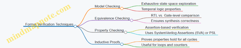
Model Checking
Model checking systematically explores all states of a design to verify if certain properties hold. Properties are expressed in temporal logic, such as “always” or “eventually” conditions. For example, you might check that a reset signal eventually deasserts or that a FIFO never overflows.
Equivalence Checking
Equivalence checking compares two representations of a design, typically RTL and synthesized netlist, to ensure they behave identically. This step catches synthesis bugs or unintended optimizations.
Property Checking
Property checking involves embedding assertions directly into your HDL code. Assertions specify expected behavior, such as “signal X must never be high when signal Y is low.” Formal tools then verify these assertions across all possible inputs.
Inductive Proofs
Inductive proofs verify that if a property holds at one state, it continues to hold in the next. This technique is useful for proving invariants in sequential logic.
Best Practices for Formal Verification
- Start Small: Begin with individual blocks or modules rather than the entire design. This reduces complexity and helps isolate issues.
- Write Clear Properties: Assertions should be straightforward and specific. Avoid vague or overly broad properties that can cause false failures.
- Use Assumptions: Formal tools need constraints to avoid exploring impossible states. Define input assumptions to focus verification on realistic conditions.
- Incremental Verification: Add properties step-by-step. Verify simple properties first, then move to more complex ones.
- Integrate with Simulation: Use formal verification alongside simulation. Formal can prove correctness where simulation tests specific cases.
Example: Verifying a Simple Arbiter
Consider a 2-input arbiter that grants access to one requester at a time. We want to verify that it never grants both requests simultaneously.
Property: “At any clock cycle, grant0 and grant1 are not both high.”
In SystemVerilog Assertions (SVA), this can be written as:
property no_double_grant;
  @(posedge clk) !(grant0 && grant1);
endproperty

assert property (no_double_grant);
The formal tool will check all possible input combinations and state transitions to confirm this property holds. If it finds a scenario where both grants are high, it will provide a counterexample waveform.
Example: Equivalence Checking Between RTL and Synthesized Netlist
Suppose you have an RTL description of a multiplier and a synthesized netlist from your FPGA vendor’s tool. Equivalence checking tools compare these two to ensure the synthesis process did not alter functionality.
If the tool reports equivalence, you gain confidence that your design’s behavior remains intact post-synthesis. If not, you investigate mismatches, which might be due to unsupported constructs or synthesis tool bugs.
Common Challenges and How to Address Them
- State Space Explosion: Large designs can overwhelm formal tools. Mitigate this by verifying smaller modules or applying input constraints.
- Over-Constraining Inputs: Too many assumptions can hide real bugs. Balance constraints carefully.
- Writing Effective Properties: Poorly written assertions can lead to false positives or negatives. Review properties with peers.
Summary
Formal verification tools provide a rigorous way to prove design correctness beyond simulation. By applying model checking, equivalence checking, and property assertions, FPGA developers can catch subtle bugs early. Starting with small modules, writing clear properties, and using assumptions effectively will make formal verification a practical part of your design flow.
9.3 Hardware-in-the-Loop (HIL) Testing and Emulation
Hardware-in-the-Loop (HIL) testing is a technique where a physical hardware component, such as an FPGA, is tested within a simulated environment that mimics real-world conditions. This approach bridges the gap between pure simulation and field testing by allowing the hardware to interact with a virtual model of the system it will operate in. The goal is to validate hardware behavior under controlled, repeatable scenarios before deployment.
Why Use HIL Testing?
- Early detection of design flaws: HIL allows you to test hardware responses to a wide range of inputs and fault conditions that might be difficult to replicate in the field.
- Reduced development time: By integrating hardware with simulation, you can iterate faster without waiting for full system availability.
- Cost efficiency: Testing in a simulated environment reduces the risk of damaging expensive hardware or systems during early testing phases.
Core Components of HIL Testing
Mind Map: HIL Testing Setup
Step-by-Step HIL Testing Process
- Model Creation: Develop a real-time model of the system or environment the FPGA will interact with. This could be a motor controller, communication protocol, or sensor array.
- Interface Setup: Connect the FPGA to the real-time simulator through appropriate I/O hardware, ensuring signal levels and timing align.
- Test Scenario Definition: Define input stimuli and expected outputs, including normal operation and edge cases.
- Execution: Run the FPGA in the loop, feeding it simulated inputs and monitoring outputs.
- Data Collection and Analysis: Capture responses and compare them against expected results to identify discrepancies.
Example: Testing an FPGA-Based Motor Controller
Suppose you have designed an FPGA module that controls a three-phase motor. Instead of connecting the FPGA to an actual motor, you use a real-time simulator that models the motor’s electrical and mechanical behavior.
- The simulator sends sensor signals (e.g., rotor position, current feedback) to the FPGA.
- The FPGA processes these inputs and outputs PWM signals to control the motor.
- The simulator receives these PWM signals and updates the motor model accordingly.
- Fault conditions such as sudden load changes or sensor failures can be injected to observe FPGA response.
This setup allows thorough validation of control algorithms and hardware timing without risking physical hardware.
Mind Map: Motor Controller HIL Example
Best Practices for HIL Testing
- Synchronize clocks: Ensure the FPGA and simulator run on compatible timing domains to avoid data misalignment.
- Use realistic models: The accuracy of your HIL test depends on the fidelity of the system model.
- Automate tests: Script test sequences to enable repeatability and regression testing.
- Monitor latency: Measure and minimize communication delays between FPGA and simulator.
- Incorporate fault scenarios: Test how the FPGA handles unexpected or erroneous inputs.
Emulation vs. HIL Testing
While HIL testing involves real hardware interacting with a simulated environment, emulation often refers to running the FPGA design on a hardware emulator that mimics the FPGA’s behavior before actual fabrication. Emulation is useful for verifying logic correctness and timing at scale, whereas HIL focuses on system-level interaction and real-time response.
Example: Emulating a Network Packet Processor
Before deploying a packet processing FPGA design, you might emulate the design on a hardware emulator that can run at a slower speed but allows detailed debugging. Once the design passes emulation, you move to HIL testing where the FPGA interacts with a simulated network traffic generator to validate throughput and latency under realistic conditions.
Mind Map: Emulation vs HIL
In summary, HIL testing and emulation are complementary techniques that help FPGA developers validate designs from different angles. HIL testing shines when you want to see how your FPGA behaves in a real-time system context, while emulation is better suited for deep design verification before hardware availability.
9.4 Best Practices for Regression Testing and Continuous Integration
Regression testing and continuous integration (CI) form the backbone of reliable FPGA development workflows. They ensure that changes in code or design do not break existing functionality and that integration of components happens smoothly and consistently. Here, we focus on best practices tailored for FPGA projects, where hardware description languages (HDLs), synthesis, place-and-route, and simulation all play roles.
Why Regression Testing Matters in FPGA Design
Regression testing verifies that new changes do not introduce bugs into previously working designs. In FPGA projects, this means re-running simulations, synthesis checks, and possibly hardware tests after each change. Because FPGA designs often involve complex timing and resource constraints, even small code tweaks can have unexpected effects.
Key Elements of Regression Testing for FPGA
- Automated Testbenches: Use scripted testbenches that run a suite of tests covering different modules and corner cases.
- Version Control Integration: Trigger regression tests automatically on code commits or merges.
- Incremental Testing: Focus on affected modules first, then run full regression periodically.
- Result Comparison: Use waveform or log comparison tools to detect deviations.
Continuous Integration in FPGA Development
CI automates the build, test, and verification pipeline. For FPGA, this includes:
- HDL linting and style checks
- Simulation runs (behavioral and timing)
- Synthesis and implementation checks
- Bitstream generation (optional, depending on time constraints)
- Hardware-in-the-loop tests (if available)
Best Practices for Regression Testing and CI
Automate Everything You Can
Manual testing is error-prone and slow. Use scripts to run simulations, synthesis, and checks. Tools like Makefiles, Python scripts, or CI platforms (Jenkins, GitLab CI) can orchestrate these steps.
Keep Testbenches Modular and Reusable
Design testbenches as modular blocks that can be combined or extended. Parameterize inputs and expected outputs to cover a wide range of scenarios without rewriting code.
Prioritize Tests Based on Impact
Not every change requires a full regression run. Use dependency analysis or tagging to run quick smoke tests on affected modules, then schedule full regression overnight or before releases.
Maintain a Baseline for Comparison
Store golden results for simulations and synthesis reports. Automated comparison scripts should flag differences beyond acceptable thresholds.
Integrate Linting and Static Analysis
Catch style violations and common errors early. This reduces the chance of subtle bugs slipping into the regression tests.
Use Incremental Builds Where Possible
Full synthesis and place-and-route can be time-consuming. Incremental builds speed up feedback loops by reusing previous results when possible.
Log and Report Clearly
CI systems should provide clear, concise reports on test outcomes. Highlight failures with links to logs, waveforms, or synthesis reports.
Include Hardware Testing When Feasible
If you have access to FPGA boards, automate flashing and running hardware tests. This closes the loop between simulation and real-world behavior.
Mind Map: Regression Testing Workflow
Mind Map: Continuous Integration Pipeline for FPGA
Example: Setting Up a Simple Regression Test for a FIFO Module
Suppose you have a FIFO module written in Verilog. Your regression test should:
- Include a testbench that writes and reads various data patterns.
- Check for underflow and overflow conditions.
- Run simulations automatically on each commit.
A Python script could automate running the simulator (e.g., ModelSim or QuestaSim), capture output logs, and compare them against expected results. If differences appear, the script flags the test as failed and sends a notification.
Example: CI Pipeline Snippet Using GitLab CI
stages:
  - lint
  - simulate
  - synthesize

lint_hdl:
  stage: lint
  script:
    - hdl_linter fifo.v
  only:
    - master

simulate_fifo:
  stage: simulate
  script:
    - vsim -c -do run_fifo_test.do
    - python compare_results.py
  only:
    - master

synthesize_fifo:
  stage: synthesize
  script:
    - quartus_sh --flow compile fifo_project
  only:
    - master
This pipeline runs linting, simulation, and synthesis sequentially on the master branch. The simulation step includes a script to compare output logs, ensuring regression tests catch any functional deviations.
Wrapping Up
Regression testing and continuous integration are not just about automation but about building confidence in your FPGA designs. By structuring tests thoughtfully, automating processes, and integrating tools effectively, you reduce risk and speed up development cycles. The key is to balance thoroughness with efficiency—running enough tests to catch issues without bogging down your workflow.
9.5 Example: Verifying a Complex DSP Pipeline Using UVM
Verifying a complex DSP (Digital Signal Processing) pipeline using UVM (Universal Verification Methodology) requires a structured approach that balances thoroughness with efficiency. The goal is to ensure the DSP pipeline behaves correctly under all expected conditions, including corner cases, while maintaining manageable verification effort.
Overview of the DSP Pipeline Verification
A typical DSP pipeline might include stages such as filtering, FFT (Fast Fourier Transform), scaling, and accumulation. Each stage transforms data, and errors can propagate downstream. Verification must cover functional correctness, timing, and data integrity.
Key Components of the UVM Testbench for DSP Pipeline
- Driver: Sends stimulus to the DUT (Device Under Test) inputs.
- Monitor: Observes DUT outputs and internal signals.
- Scoreboard: Compares DUT outputs against expected results.
- Sequencer: Controls the sequence of stimulus transactions.
- Agent: Encapsulates driver, monitor, and sequencer.
- Environment: Instantiates and connects agents and scoreboard.
Mind Map: UVM Testbench Structure for DSP Pipeline

Step 1: Define Transactions
Transactions represent data packets flowing through the pipeline. For a DSP pipeline, a transaction might include fields like input samples, control signals, and expected output.
class dsp_transaction extends uvm_sequence_item;
  rand bit [15:0] sample_in;
  rand bit [3:0]  control_flags;
  bit [31:0] expected_out;

  `uvm_object_utils(dsp_transaction)

  function new(string name = "dsp_transaction");
    super.new(name);
  endfunction
endclass
Step 2: Create Sequences
Sequences generate ordered transactions to stimulate the DUT. For example, a filter sequence might generate a set of input samples with varying frequencies.
class filter_sequence extends uvm_sequence #(dsp_transaction);
  `uvm_object_utils(filter_sequence)

  function new(string name = "filter_sequence");
    super.new(name);
  endfunction

  task body();
    dsp_transaction tr;
    foreach (int i [0:99]) begin
      tr = dsp_transaction::type_id::create("tr");
      tr.sample_in = $urandom_range(0, 65535);
      tr.control_flags = 4'b0001; // Filter enable
      start_item(tr);
      finish_item(tr);
    end
  endtask
endclass
Step 3: Implement Driver and Monitor
The driver converts transactions into pin-level signals. The monitor samples outputs and converts them back into transactions for checking.
class dsp_driver extends uvm_driver #(dsp_transaction);
  virtual dsp_if vif;

  function new(string name, uvm_component parent);
    super.new(name, parent);
  endfunction

  task run_phase(uvm_phase phase);
    dsp_transaction tr;
    forever begin
      seq_item_port.get_next_item(tr);
      vif.sample_in <= tr.sample_in;
      vif.control <= tr.control_flags;
      @(posedge vif.clk);
      seq_item_port.item_done();
    end
  endtask
endclass

class dsp_monitor extends uvm_monitor;
  virtual dsp_if vif;
  uvm_analysis_port #(dsp_transaction) analysis_port = new("analysis_port", this);

  function new(string name, uvm_component parent);
    super.new(name, parent);
  endfunction

  task run_phase(uvm_phase phase);
    dsp_transaction tr;
    forever begin
      @(posedge vif.clk);
      tr = dsp_transaction::type_id::create("tr");
      tr.sample_in = vif.sample_in;
      tr.control_flags = vif.control;
      tr.expected_out = vif.output_data;
      analysis_port.write(tr);
    end
  endtask
endclass
Step 4: Scoreboard Implementation
The scoreboard compares observed outputs with expected results. For a DSP pipeline, it might run a software model of the pipeline to generate expected outputs.
class dsp_scoreboard extends uvm_component;
  uvm_analysis_imp #(dsp_transaction, dsp_scoreboard) analysis_export;
  mailbox #(dsp_transaction) expected_mb = new();

  function new(string name, uvm_component parent);
    super.new(name, parent);
    analysis_export = new("analysis_export", this);
  endfunction

  function void write(dsp_transaction tr);
    dsp_transaction expected_tr = expected_mb.get();
    if (tr.expected_out !== expected_tr.expected_out) begin
      `uvm_error("SCOREBOARD", $sformatf("Mismatch: got %0h, expected %0h", tr.expected_out, expected_tr.expected_out))
    end else begin
      `uvm_info("SCOREBOARD", "Output matches expected result", UVM_LOW)
    end
  endfunction
endclass
Step 5: Integrate and Run the Test
The environment instantiates agents and scoreboard, connects analysis ports, and runs sequences.
class dsp_env extends uvm_env;
  dsp_agent agent;
  dsp_scoreboard scoreboard;

  function new(string name, uvm_component parent);
    super.new(name, parent);
  endfunction

  function void build_phase(uvm_phase phase);
    super.build_phase(phase);
    agent = dsp_agent::type_id::create("agent", this);
    scoreboard = dsp_scoreboard::type_id::create("scoreboard", this);
  endfunction

  function void connect_phase(uvm_phase phase);
    super.connect_phase(phase);
    agent.monitor.analysis_port.connect(scoreboard.analysis_export);
  endfunction
endclass

class dsp_test extends uvm_test;
  dsp_env env;

  function new(string name = "dsp_test");
    super.new(name);
  endfunction

  function void build_phase(uvm_phase phase);
    super.build_phase(phase);
    env = dsp_env::type_id::create("env", this);
  endfunction

  task run_phase(uvm_phase phase);
    filter_sequence filter_seq = filter_sequence::type_id::create("filter_seq");
    phase.raise_objection(this);
    filter_seq.start(env.agent.sequencer);
    phase.drop_objection(this);
  endtask
endclass
Summary
Verifying a complex DSP pipeline with UVM involves creating a layered testbench that mimics the data flow through the pipeline. Transactions represent data units, sequences generate stimulus, drivers and monitors handle interface signals, and the scoreboard checks correctness. The modularity of UVM allows you to isolate each pipeline stage and verify it independently or in combination, making debugging and coverage analysis more manageable.
This example demonstrates how to structure verification components and provides a foundation to expand with more detailed stimulus, coverage, and corner case testing.
10. Power Management and Thermal Considerations
10.1 Power Estimation and Analysis Tools
Power estimation and analysis are essential steps in FPGA design, especially when power budgets are tight or thermal constraints are critical. Getting a handle on power consumption early helps avoid costly redesigns and ensures the device runs reliably within its limits.
What is Power Estimation?
Power estimation is the process of predicting how much power your FPGA design will consume before or during implementation. It includes static power (leakage currents when the device is idle) and dynamic power (power used when the device is switching).
Why Estimate Power?
- To verify that the design meets power budgets.
- To identify power-hungry blocks for optimization.
- To plan thermal management strategies.
Types of Power in FPGA Designs
- Static Power: Leakage currents in transistors, largely dependent on device technology and temperature.
- Dynamic Power: Power consumed during signal transitions and clock toggling.
- I/O Power: Power used by input/output buffers, often significant in high-speed designs.
Power Estimation Workflow Mind Map
Tools and Techniques
Most FPGA vendors provide power estimation tools integrated into their design suites. These tools use a combination of analytical models and switching activity data to estimate power.
- Early Estimation: Uses design parameters like resource utilization and clock frequency. It’s fast but less accurate.
- Post-Implementation Estimation: Uses detailed switching activity from simulation or real hardware, providing more precise results.
Example: Estimating Power for a Simple FIR Filter
Suppose you design a 16-tap FIR filter in Verilog targeting a Xilinx Ultrascale+ FPGA.
- Early Estimation: After synthesis, the tool reports resource usage and clock frequency. Using these, the power estimator predicts 1.2 W total power.
- Simulation: Run a testbench with realistic input data and generate a Switching Activity Interchange Format (SAIF) file.
- Post-Implementation Estimation: Import the SAIF file into the power analysis tool. It reports 1.5 W total power, with 60% dynamic power and 40% static power.
- Analysis: The tool highlights that the multiplier blocks consume the most dynamic power.
- Optimization: Introduce clock gating on multiplier blocks when idle, reducing dynamic power by 20% in the next iteration.
Key Parameters Affecting Power Estimation
- Toggle Rate: How often signals change state. Higher toggle rates increase dynamic power.
- Clock Frequency: Higher frequency means more switching events per second.
- Resource Utilization: More logic elements switching means more power.
- Voltage: Power scales roughly with the square of voltage.
Power Estimation Mind Map: Factors Influencing Power
Practical Tips
- Generate switching activity files from realistic workloads to get meaningful estimates.
- Use hierarchical power reports to focus optimization efforts on the most power-hungry blocks.
- Remember static power can be significant in modern FPGAs, especially at high temperatures.
- Consider I/O power separately, especially for designs with many high-speed interfaces.
In summary, power estimation is a multi-step process combining design data, simulation results, and vendor tools. It provides actionable insights that guide design decisions to meet power and thermal targets without guesswork.
10.2 Dynamic Voltage and Frequency Scaling (DVFS) on FPGA
Dynamic Voltage and Frequency Scaling (DVFS) is a technique used to adjust the voltage and clock frequency of an FPGA dynamically, based on workload demands, to optimize power consumption and thermal performance. Unlike fixed-frequency operation, DVFS allows the FPGA to run at the lowest possible power state while still meeting performance requirements.
Why DVFS Matters on FPGAs
FPGAs are often deployed in environments where power efficiency is critical, such as embedded systems, portable devices, or data centers with strict thermal budgets. Since power consumption in CMOS circuits roughly scales with the square of the supply voltage and linearly with frequency, reducing either can significantly cut power usage.
However, lowering voltage reduces the maximum achievable frequency, so DVFS balances these parameters to maintain system performance while saving power.
Core Concepts of DVFS on FPGA
Voltage Scaling
Voltage scaling involves adjusting the FPGA’s core voltage (Vccint) or I/O voltages dynamically. This requires hardware support such as programmable voltage regulators capable of fast transitions. Lowering voltage reduces dynamic power consumption but also slows transistor switching speeds, which limits maximum frequency.
Example:
Suppose an FPGA normally operates at 1.0 V and 200 MHz for a given workload. If the workload decreases, the voltage can be dropped to 0.85 V, but the maximum frequency might then be limited to 150 MHz. The system can reduce frequency accordingly to maintain timing margins.
Frequency Scaling
Frequency scaling adjusts the clock frequency driving the FPGA logic. Modern FPGAs provide clock management resources like PLLs (Phase-Locked Loops) and MMCMs (Mixed-Mode Clock Managers) that can generate multiple clock frequencies and support dynamic reconfiguration.
Dynamic frequency scaling can be achieved by:
- Switching between pre-configured clock frequencies.
- Adjusting PLL/MMCM parameters on the fly.
Example:
An FPGA design uses a PLL to generate a 250 MHz clock. When the workload is low, the PLL is reconfigured to output 125 MHz, halving the frequency and reducing dynamic power.
Control Mechanisms
DVFS requires a control system to decide when and how to adjust voltage and frequency. This can be implemented in hardware, software, or a combination:
- Workload Monitoring: Metrics like utilization counters, temperature sensors, or performance counters inform the control logic.
- Feedback Loops: Closed-loop systems adjust voltage and frequency based on real-time measurements.
- Control Algorithms: Simple threshold-based or more complex PID controllers can be used.
Example:
A hardware monitor counts the number of active processing elements. If utilization drops below 30%, the controller lowers frequency and voltage; if it rises above 70%, it ramps them back up.
Implementation Challenges
- Voltage Transition Latency: Switching voltage levels is not instantaneous and may require careful sequencing to avoid instability.
- Frequency Switching Glitches: Changing clock frequency dynamically can introduce glitches or timing violations if not managed properly.
- Timing Closure: Designs must be verified to meet timing across all voltage and frequency operating points.
Practical Example: Implementing DVFS in a Signal Processing FPGA
- Setup: The FPGA runs a digital filter processing streaming data. Under peak load, it runs at 1.0 V and 200 MHz.
- Monitoring: A utilization counter tracks the filter’s processing load every 10 ms.
- Decision Logic: If utilization < 40%, the controller triggers a frequency reduction to 150 MHz and voltage drop to 0.9 V.
- Transition: The voltage regulator adjusts the core voltage, and the PLL reconfigures to the lower frequency.
- Verification: Timing analysis confirms the design meets timing at 0.9 V and 150 MHz.
- Result: Power consumption drops by approximately 30% during low workload periods without impacting output quality.
Summary
DVFS on FPGA is a balancing act between power savings and performance. It requires coordinated voltage regulators, clock management, and control logic. While it adds complexity, the power and thermal benefits can be substantial, especially in systems with variable workloads. Careful design and validation ensure stable operation across all voltage-frequency points.
10.3 Thermal Management Techniques and Cooling Solutions
Managing heat in FPGA designs is essential to maintain performance, reliability, and longevity. FPGAs can generate significant heat due to high switching activity, dense logic, and embedded blocks like DSPs and memory. Without proper thermal management, devices may throttle, malfunction, or fail prematurely.
Understanding Heat Sources in FPGA
- Dynamic Power Dissipation: Heat generated by switching transistors during operation.
- Static Power Dissipation: Leakage currents even when the device is idle.
- Power Density: Concentration of power in small areas, especially in high-utilization regions.
Key Thermal Management Techniques
Thermal Management Techniques Mind Map
Passive Cooling
-
Heat Sinks: Metal blocks attached to the FPGA package to dissipate heat by conduction and convection. The choice of heat sink depends on size constraints and thermal resistance requirements.
-
Thermal Interface Materials (TIM): Materials like thermal pads or pastes improve heat transfer between the FPGA and heat sink by filling microscopic gaps.
-
PCB Thermal Design: Using thermal vias, copper pours, and multi-layer boards to spread heat away from the FPGA. Placing heat-generating components strategically reduces hotspots.
Active Cooling
-
Fans: Forced airflow over heat sinks or the FPGA package increases convective heat transfer. Fan speed can be adjusted based on temperature readings.
-
Liquid Cooling: Circulates coolant through cold plates attached to the FPGA or system. More complex and costly but effective for high-power designs.
Thermal Monitoring
- On-chip Sensors: Modern FPGAs include temperature sensors that provide real-time data for dynamic thermal management.
- External Sensors: Thermocouples or infrared sensors can monitor board or system temperature.
Thermal Simulation and Analysis
- Computational Fluid Dynamics (CFD) tools model airflow and heat dissipation.
- Thermal modeling during design helps identify hotspots and optimize cooling solutions before hardware fabrication.
Example: Designing Thermal Management for a High-Performance FPGA
Suppose you have an FPGA design consuming 15W in a compact enclosure. The goal is to keep the FPGA junction temperature below 85°C.
-
Estimate Thermal Resistance: Calculate the maximum allowable thermal resistance from junction to ambient \(R_ja\) using:
\[ R_{ja} = \frac{T_{junction_max} - T_{ambient}}{Power} \]
Assuming ambient at 40°C:
\[ R_{ja} = \frac{85 - 40}{15} = 3 °C/W \]
-
Select Heat Sink: Choose a heat sink with thermal resistance less than 3°C/W, considering TIM and PCB contributions.
-
Add Fan: If passive cooling alone doesn’t meet requirements, add a fan to reduce thermal resistance.
-
Use Thermal Vias: Implement thermal vias under the FPGA to spread heat into inner PCB layers.
-
Monitor Temperature: Use on-chip sensors to adjust fan speed dynamically.
Practical Tips
- Always verify thermal solutions with real measurements, not just simulations.
- Avoid placing heat-sensitive components near the FPGA hot spots.
- Consider airflow direction and obstructions in the enclosure.
- Use thermal grease or pads sparingly but effectively to avoid air gaps.
Cooling Solutions Mind Map
Thermal management is a balance between cost, complexity, and performance. Simple passive cooling may suffice for low-power designs, while high-performance or dense FPGA systems often require active or hybrid solutions. Monitoring and iterative testing ensure the cooling approach meets the design’s thermal goals.
10.4 Best Practices for Low-Power FPGA Design
Low-power design in FPGA development is a practical necessity, especially as devices grow more complex and power budgets tighten. The goal is to reduce dynamic and static power consumption without sacrificing performance or functionality. Here’s a structured approach to best practices for low-power FPGA design, supported by examples and mind maps to clarify key concepts.
Key Areas to Target for Low-Power FPGA Design
Clock Management
Clock signals toggle frequently and drive much of the dynamic power consumption. Managing clocks efficiently is one of the most effective ways to reduce power.
-
Clock Gating: Disable the clock to registers or modules when they are not in use. For example, if a processing block is idle during certain cycles, gating its clock prevents unnecessary toggling.
-
Clock Domain Reduction: Consolidate multiple clock domains where possible to reduce the number of active clocks. Fewer clocks mean fewer toggling signals and less power.
Example: In a video processing pipeline, the frame rate might be 30 fps, but some blocks only need to operate at 15 fps. By gating the clock to these blocks during inactive periods, power consumption can be cut significantly.
Logic Optimization
Reducing the amount of switching activity in combinational and sequential logic lowers dynamic power.
-
Resource Sharing: Instead of instantiating multiple identical functional units, share one unit across multiple operations scheduled at different times.
-
Minimizing Switching Activity: Use encoding techniques or redesign logic to reduce bit toggling. For instance, Gray code counters toggle only one bit per increment, reducing switching compared to binary counters.
Example: A design requiring multiple multipliers can use a single multiplier unit with multiplexed inputs and control logic, trading off throughput for lower power.
Power-Aware Synthesis
Synthesis tools offer options to optimize for power.
-
Retiming: Moves registers to reduce critical path delays and can also reduce switching activity by balancing logic.
-
Register Balancing: Ensures that registers toggle only when necessary, avoiding unnecessary transitions.
Example: Enabling power optimization during synthesis in tools like Vivado or Quartus can automatically insert clock gating and optimize logic to reduce power.
Voltage and Frequency Scaling
Adjusting supply voltage and clock frequency directly impacts power consumption.
-
Dynamic Voltage Scaling (DVS): Lowering the voltage reduces power quadratically but requires careful timing margin analysis.
-
Dynamic Frequency Scaling (DFS): Reducing clock frequency lowers dynamic power linearly.
Example: In a sensor data acquisition system, the FPGA can run at full speed only during data bursts and switch to a lower frequency and voltage during idle periods.
Power-Aware Floorplanning
Physical placement of logic affects power by influencing interconnect length and switching capacitance.
-
Grouping High-Activity Logic: Place modules that communicate heavily close to each other to reduce interconnect power.
-
Minimizing Interconnect Length: Shorter routing reduces capacitance and thus dynamic power.
Example: In a multi-core FPGA design, grouping cores that exchange data frequently reduces power spent on long interconnects.
Use of Low-Power IP Cores
Many FPGA vendors provide IP cores optimized for low power. Using these cores instead of custom implementations can save power and design time.
Example: Using vendor-provided DSP blocks or memory controllers that include power-saving features.
Power Analysis and Monitoring
Early and continuous power estimation helps identify hotspots and validate power-saving measures.
-
Early Estimation: Use synthesis and simulation tools to estimate power before implementation.
-
Post-Implementation Analysis: Analyze power reports after place-and-route to confirm savings.
Example: Running power simulations with realistic toggle rates from testbenches to identify modules with unexpectedly high power.
Mind Map: Low-Power FPGA Design Best Practices
Concrete Example: Implementing Clock Gating in a Data Processing Module
Suppose you have a module that processes data only when a valid input signal is high. Instead of letting the clock run continuously, you can gate the clock using the valid signal:
module clock_gated_processor(
  input wire clk,
  input wire reset,
  input wire data_valid,
  input wire [7:0] data_in,
  output reg [7:0] data_out
);

  wire gated_clk;

  // Simple clock gating cell
  assign gated_clk = clk & data_valid;

  always @(posedge gated_clk or posedge reset) begin
    if (reset)
      data_out <= 8'd0;
    else
      data_out <= data_in + 1; // example operation
  end

endmodule
This approach ensures the internal registers toggle only when processing valid data, reducing dynamic power.
Summary
Low-power FPGA design is about making deliberate choices at every stage: from clock management to logic optimization, synthesis settings, and physical layout. Each technique contributes to reducing power consumption without compromising the design’s goals. Applying these practices consistently leads to efficient, power-conscious FPGA implementations.
10.5 Example: Implementing Power Gating in a Multi-Clock Domain Design
Power gating is a technique used to reduce static power consumption by shutting off power to idle blocks of logic. When dealing with multi-clock domain designs, power gating requires careful coordination to avoid data corruption, clock domain crossing issues, and ensure safe power-up and power-down sequences.
Understanding the Challenge
In a multi-clock domain design, different parts of the FPGA logic run on separate clocks, often asynchronous to each other. Power gating a block in one clock domain while others remain active can cause:
- Loss of data if registers are powered down unexpectedly.
- Metastability if signals cross into powered-down domains.
- Difficulty in synchronizing power-up sequences.
The goal is to implement power gating such that each clock domain can be independently powered down and up without causing system instability.
Key Steps in Implementing Power Gating
-
Partition the Design into Power Domains
- Identify logic blocks that can be independently powered down.
- Group registers and combinational logic into these domains.
-
Insert Power Gating Cells
- Use FPGA vendor-specific power gating primitives or emulate gating by clock gating and retention registers.
-
Manage Clock Domains
- Use clock gating or clock enable signals to disable clocks safely before power gating.
- Ensure no active clock edges occur during power-down.
-
Implement Retention Registers
- Preserve critical state across power cycles.
-
Synchronize Power-Up and Power-Down Signals
- Use handshake signals between domains.
- Employ synchronizers to avoid metastability.
-
Verify with Simulation and On-Hardware Testing
- Check timing, data integrity, and power consumption.
Mind Map: Power Gating Implementation Workflow
Example: Power Gating a Processing Block with Two Clock Domains
Consider a design with two clock domains:
- CLK_A: 100 MHz domain running a data processing block.
- CLK_B: 50 MHz domain running control logic.
We want to power gate the processing block (CLK_A domain) when idle, without affecting the control logic (CLK_B domain).
Step 1: Clock Gating
Before power gating, disable the clock to the processing block to prevent clock edges during power-down.
// Clock gating enable signal
reg clk_a_enable;

// Gated clock generation
assign gated_clk_a = clk_a & clk_a_enable;
Step 2: Retention Registers
Use retention registers to save the state of critical registers before power-down.
reg [7:0] data_reg, data_reg_retention;

always @(posedge gated_clk_a or negedge reset_n) begin
  if (!reset_n) begin
    data_reg <= 8'd0;
  end else if (power_down) begin
    data_reg_retention <= data_reg; // Save state
  end else if (power_up) begin
    data_reg <= data_reg_retention; // Restore state
  end else begin
    data_reg <= data_reg + 1;
  end
end
Step 3: Power Gating Control Logic
Control signals coordinate the power gating sequence.
reg power_down, power_up;

// State machine for power gating
always @(posedge clk_b or negedge reset_n) begin
  if (!reset_n) begin
    power_down <= 0;
    power_up <= 0;
    clk_a_enable <= 1;
  end else begin
    if (idle_condition) begin
      power_down <= 1;
      clk_a_enable <= 0; // Disable clock before power gating
    end else if (wake_condition) begin
      power_up <= 1;
      clk_a_enable <= 1; // Enable clock after power-up
      power_down <= 0;
    end
  end
end
Step 4: Synchronization Between Domains
Use synchronizers to safely transfer power gating control signals between CLK_B and CLK_A domains.
// Synchronizer for power_down signal
reg [1:0] power_down_sync;
always @(posedge gated_clk_a or negedge reset_n) begin
  if (!reset_n) power_down_sync <= 2'b00;
  else power_down_sync <= {power_down_sync[0], power_down};
end
wire power_down_clk_a = power_down_sync[1];
Step 5: Verification
- Simulate the power gating sequence ensuring no data corruption.
- Confirm that the clock is disabled before power gating.
- Validate state retention and restoration.
Mind Map: Example Implementation Details
Final Notes
Power gating in multi-clock domain designs is a balancing act between power savings and system stability. Clock gating combined with retention registers provides a practical approach when dedicated power gating cells are unavailable. Synchronization and careful sequencing prevent metastability and data loss. Testing at both simulation and hardware levels is essential to confirm the design’s robustness.
This example provides a foundation that can be expanded for more complex systems with multiple power domains and asynchronous clocks.
11. Security Techniques in FPGA Designs
11.1 Understanding FPGA Security Threats and Vulnerabilities
FPGA security is a critical topic that often gets overlooked until a breach or failure occurs. Unlike fixed-function devices, FPGAs are reprogrammable, which adds flexibility but also opens up unique security challenges. Understanding these threats and vulnerabilities is essential for anyone designing or deploying FPGA-based systems.
Key Security Threats in FPGA Systems
- Bitstream Interception and Tampering: The configuration bitstream is the blueprint that programs the FPGA. If an attacker gains access to it, they can reverse-engineer the design, inject malicious logic, or clone the device.
- Side-Channel Attacks: These attacks exploit physical characteristics such as power consumption, electromagnetic emissions, or timing variations to extract secret information like encryption keys.
- IP Theft and Reverse Engineering: Intellectual property (IP) cores embedded in FPGA designs are valuable. Attackers may attempt to extract or replicate them by analyzing the bitstream or probing the device.
- Fault Injection Attacks: By inducing faults through voltage glitches, clock manipulation, or radiation, attackers can cause the FPGA to behave unpredictably, potentially bypassing security checks.
- Configuration Interface Attacks: Unauthorized access to configuration ports (JTAG, SPI, etc.) can allow an attacker to reprogram or read out the FPGA.
- Malicious Hardware Trojans: Hidden circuits inserted during design or manufacturing can activate under certain conditions to leak data or disrupt operation.
Mind Map: FPGA Security Threats
Examples Illustrating FPGA Security Vulnerabilities
-
Bitstream Interception Example: Suppose an FPGA in a secure communications device loads its bitstream from an external flash memory. If the flash memory is not encrypted or access-controlled, an attacker with physical access could read the bitstream, analyze the design, and create counterfeit devices or find vulnerabilities.
-
Side-Channel Attack Example: An FPGA implementing AES encryption might leak information through power consumption patterns. By measuring the power draw during encryption operations, an attacker can perform differential power analysis to recover the secret key.
-
Fault Injection Example: In a system where the FPGA checks authentication tokens, an attacker might use voltage glitching to skip the token verification logic, granting unauthorized access.
-
Configuration Interface Attack Example: If JTAG access is left enabled and unprotected on a deployed FPGA, an attacker could use it to halt the processor, read internal registers, or reprogram the device with malicious firmware.
Mind Map: Common Attack Vectors
Why These Vulnerabilities Matter
FPGAs often serve as the backbone for critical systems—communications, defense, finance, and industrial control. A breach can lead to data theft, system downtime, or even physical damage. Unlike software vulnerabilities, hardware-level attacks can be harder to detect and mitigate once deployed.
Summary
FPGA security threats cover a broad spectrum from physical attacks on the device to logical attacks on configuration and IP. Each threat requires specific countermeasures, but understanding the attack surface is the first step. Protecting the bitstream, securing configuration interfaces, and guarding against side-channel and fault injection attacks are foundational practices in FPGA security design.
11.2 Bitstream Encryption and Authentication Methods
FPGA bitstream encryption and authentication are essential for protecting intellectual property and preventing unauthorized device configuration. Bitstreams are the binary files that configure the FPGA fabric, and if exposed or altered, they can lead to security breaches or IP theft. This section covers the main methods to secure bitstreams, practical considerations, and examples.
Why Encrypt and Authenticate Bitstreams?
- Confidentiality: Prevents reverse engineering by encrypting the bitstream data.
- Integrity: Ensures the bitstream has not been tampered with.
- Authentication: Confirms the bitstream originates from a trusted source.
Core Concepts
Mind Map: Bitstream Security Methods
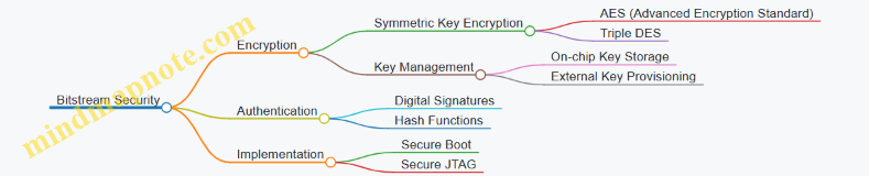
Bitstream Encryption
Encryption scrambles the bitstream data so that only authorized devices can correctly configure the FPGA. Most modern FPGAs support built-in encryption engines.
Common Algorithms:
- AES (Advanced Encryption Standard): The industry standard for symmetric encryption, typically AES-128 or AES-256.
- Triple DES: Older and less common now, but still used in some legacy systems.
How It Works:
- The bitstream is encrypted offline using a secret key.
- The encrypted bitstream is stored or transmitted.
- On power-up or configuration, the FPGA uses an internal key to decrypt the bitstream.
Key Management:
- Keys may be stored in one-time programmable (OTP) memory or battery-backed RAM inside the FPGA.
- Some systems use external secure elements or key provisioning during manufacturing.
Example:
Suppose you have a design bitstream design.bit. Using vendor tools, you encrypt it with AES-128 using a key stored in the FPGA’s OTP memory. When the FPGA powers up, it automatically decrypts the bitstream before configuration.
Bitstream Authentication
Encryption alone does not guarantee the bitstream is genuine. Authentication methods verify the source and integrity.
Digital Signatures:
- A cryptographic hash of the bitstream is created.
- The hash is signed with a private key.
- The FPGA or a secure bootloader verifies the signature using the corresponding public key.
Hash Functions:
- Common hashes include SHA-256.
- Used to detect any modification in the bitstream.
Example:
Before encryption, the bitstream is hashed and signed by the vendor’s private key. The FPGA verifies the signature at configuration time, rejecting the bitstream if verification fails.
Mind Map: Bitstream Authentication Process
Practical Considerations
- Key Security: Protecting keys is critical. Exposure can compromise all devices using the same key.
- Performance Impact: Decryption and authentication add latency during configuration but are usually negligible compared to overall system operation.
- Tool Support: Most FPGA vendors provide integrated support for encryption and authentication in their toolchains.
- Partial Reconfiguration: Encryption and authentication can be applied to partial bitstreams, but care must be taken to manage keys and regions properly.
Example Walkthrough: AES Encryption with Authentication
- Generate a 128-bit AES key and program it into the FPGA’s OTP memory.
- Use vendor tools to hash the bitstream with SHA-256.
- Sign the hash with a private RSA key.
- Append the signature to the bitstream.
- Encrypt the combined bitstream and signature using AES-128.
- Load the encrypted bitstream onto the device.
- On configuration, the FPGA decrypts the bitstream, verifies the signature, and configures only if verification passes.
This approach ensures confidentiality, integrity, and authenticity in one flow.
In summary, bitstream encryption and authentication form the backbone of FPGA security. They protect designs from unauthorized use and modification, preserving both IP and system reliability. Implementing these methods requires careful key management and understanding of the vendor’s security features, but the effort pays off in robust, secure FPGA deployments.
11.3 Secure Boot and Runtime Protection
Secure boot and runtime protection are essential components in FPGA security, ensuring that only trusted code runs on the device from power-up and throughout operation. Secure boot verifies the authenticity and integrity of the FPGA configuration bitstream and any embedded software before execution. Runtime protection maintains the system’s security posture by detecting and mitigating unauthorized changes or attacks while the FPGA is active.
Secure Boot
Secure boot starts with a root of trust, typically a small, immutable piece of code or hardware logic that cannot be altered after manufacturing. This root of trust verifies the digital signature of the FPGA bitstream or embedded processor firmware before allowing it to load. The verification process involves cryptographic checks such as RSA or ECC signatures and hash comparisons.
Key steps in secure boot:
- Root of Trust Initialization: A hardware block or immutable code segment that initiates the boot process.
- Bitstream Authentication: The FPGA bitstream is signed by the vendor or developer using a private key.
- Signature Verification: The FPGA or embedded processor uses a stored public key to verify the signature.
- Integrity Check: Hashes or checksums confirm the bitstream has not been altered.
- Conditional Loading: Only if verification passes does the FPGA configure itself.
Example: On Xilinx Zynq devices, the Platform Management Unit (PMU) acts as the root of trust. It verifies the bitstream signature stored in external flash before loading the FPGA fabric and the ARM processor’s boot image.
Runtime Protection
Once the FPGA is configured and running, runtime protection mechanisms monitor for unauthorized changes or suspicious activity. This includes detecting bitstream tampering, unauthorized reconfiguration attempts, or software exploits targeting embedded processors.
Common runtime protection techniques:
- Bitstream Scrubbing: Periodic reloading or checking of the bitstream to correct soft errors or tampering.
- Watchdog Timers: Hardware timers reset the system if abnormal behavior is detected.
- Access Control: Restricting who or what can trigger reconfiguration or access sensitive registers.
- Secure Debugging: Limiting debug access to prevent leakage of sensitive information.
Example: Intel Stratix 10 FPGAs support runtime reconfiguration with authentication checks, preventing unauthorized partial reconfiguration. Additionally, embedded processors can run security monitors that watch for abnormal memory accesses or code injections.
Mind Map: Secure Boot Process
Mind Map: Runtime Protection Techniques
Practical Example: Secure Boot on a Zynq FPGA
- Preparation: The developer signs the bitstream using a private key.
- Storage: The signed bitstream is stored in external QSPI flash.
- Boot: On power-up, the PMU reads the bitstream header and verifies the signature using the stored public key.
- Configuration: If verification passes, the FPGA fabric is configured with the bitstream.
- Failure Handling: If verification fails, the PMU halts configuration and can trigger a fallback or alert.
Practical Example: Runtime Protection via Bitstream Scrubbing
- The FPGA continuously monitors its configuration memory.
- If a single-event upset (SEU) or tampering is detected, the FPGA reloads the affected configuration frames.
- This process runs transparently without interrupting the application.
Secure boot and runtime protection form a layered defense. Secure boot stops unauthorized code from running at startup, while runtime protection guards against attacks during operation. Together, they help maintain the integrity and trustworthiness of FPGA-based systems.
11.4 Best Practices for Designing Secure FPGA Systems
Designing secure FPGA systems requires a layered approach that addresses vulnerabilities at multiple levels: design, implementation, and deployment. Below is a structured overview of best practices, accompanied by mind maps and examples to clarify key points.
Secure Design Principles
- Least Privilege: Limit access rights for components and users to the minimum necessary.
- Defense in Depth: Use multiple security layers so that if one fails, others still protect the system.
- Fail-Safe Defaults: Default configurations should be secure, requiring explicit action to reduce security.
Secure Design Principles Mind Map
Example: When designing an FPGA system with multiple IP blocks, restrict communication paths so that only authorized blocks can exchange data. For instance, an encryption module should not be accessible by debugging interfaces.
Bitstream Protection
- Encryption: Encrypt the bitstream to prevent unauthorized copying or reverse engineering.
- Authentication: Use cryptographic signatures to verify bitstream integrity before configuration.
- Key Management: Store keys securely, preferably in tamper-resistant hardware or secure enclaves.
Bitstream Protection Mind Map
Example: On Xilinx devices, enable AES-256 bitstream encryption and use the device’s secure key storage to prevent extraction. This ensures that even if the bitstream is intercepted, it cannot be loaded onto another device.
Secure Boot and Configuration
- Chain of Trust: Establish a verified boot process starting from immutable hardware roots.
- Configuration Integrity: Verify bitstream authenticity at each configuration stage.
- Rollback Protection: Prevent loading older, potentially vulnerable bitstreams.
Secure Boot and Configuration Mind Map
Example: Implement a bootloader that verifies the FPGA bitstream signature before programming. If verification fails, the system halts or reverts to a known good configuration.
Side-Channel Attack Mitigation
- Power Analysis Resistance: Balance power consumption or add noise to obscure cryptographic operations.
- Timing Attack Prevention: Ensure operations execute in constant time regardless of input.
- Physical Shielding: Use packaging and layout techniques to reduce electromagnetic leakage.
Side-Channel Attack Mitigation Mind Map
Example: In a cryptographic accelerator, insert random delays and balance logic paths to prevent attackers from deducing keys through power consumption patterns.
Access Control and Debug Interface Security
- Disable Unused Interfaces: Turn off JTAG or other debug ports when not in use.
- Authentication for Debug Access: Require secure authentication before enabling debug features.
- Monitor Access Attempts: Log and respond to unauthorized access attempts.
Access Control and Debug Interface Security Mind Map
Example: Configure the FPGA to disable JTAG after production programming, or protect it with a password. This prevents attackers from reading internal states or injecting faults.
Secure IP Integration
- IP Source Verification: Use IP from trusted vendors and verify signatures.
- Isolation: Separate third-party IP from critical logic using hardware boundaries.
- Regular Updates: Patch IP cores to fix known vulnerabilities.
Secure IP Integration Mind Map
Example: When integrating a third-party communication IP, place it in a dedicated region with controlled interfaces to prevent it from accessing sensitive data paths.
Runtime Monitoring and Response
- Anomaly Detection: Implement monitors to detect unusual behavior or faults.
- Fault Injection Resistance: Design logic to detect and handle faults gracefully.
- Secure Logging: Record security events for audit without exposing sensitive data.
Runtime Monitoring and Response Mind Map
Example: Add watchdog timers and error detection codes that trigger system resets or alerts if unexpected states occur, preventing prolonged exploitation.
Summary Table of Best Practices
| Practice Area | Key Actions | Example Application |
|---|---|---|
| Secure Design Principles | Least privilege, defense in depth | Restrict IP communication paths |
| Bitstream Protection | Encryption, authentication, key management | AES-256 encrypted bitstream on Xilinx |
| Secure Boot | Chain of trust, integrity checks, rollback | Verified bootloader for bitstream loading |
| Side-Channel Mitigation | Power balancing, timing consistency, shielding | Random delays in crypto accelerator |
| Debug Interface Security | Disable unused ports, authentication, logging | Password-protected JTAG |
| Secure IP Integration | Source verification, isolation, updates | Isolated third-party communication IP |
| Runtime Monitoring | Anomaly detection, fault resistance, logging | Watchdog timers and error detection codes |
Applying these practices consistently helps build FPGA systems that resist a wide range of attacks. Each layer adds complexity for an attacker, increasing the overall security posture without sacrificing performance or flexibility.
11.5 Example: Implementing a Secure Key Storage Module
Storing cryptographic keys securely on an FPGA requires careful design to protect against both physical and logical attacks. This example walks through a practical approach to implementing a secure key storage module, focusing on confidentiality, integrity, and controlled access.
Key Design Objectives
- Confidentiality: Keys must be stored in a way that prevents unauthorized reading.
- Integrity: The stored key should not be altered without detection.
- Access Control: Only authorized modules or processes can retrieve or use the key.
- Tamper Resistance: The design should detect or resist attempts to extract keys via side channels or physical probing.
High-Level Architecture Mind Map
Step 1: Selecting Storage Medium
FPGA internal Block RAM (BRAM) is a common choice for key storage, but it is volatile and readable if the design is not protected. To enhance security:
- Store keys in encrypted form inside BRAM.
- Use device-specific one-time programmable (OTP) memory or eFuses if available for storing root keys.
Example: Use a root key stored in OTP to decrypt the actual key stored in BRAM at runtime.
Step 2: Encryption and Decryption Engine
Implement a lightweight AES-128 core to encrypt keys before storage and decrypt on access. This engine uses the root key from OTP to unwrap the stored key.
Example Verilog snippet for AES key unwrapping interface:
module key_unwrapper(
  input wire clk,
  input wire rst_n,
  input wire [127:0] wrapped_key,
  input wire start,
  output reg [127:0] unwrapped_key,
  output reg done
);
  // AES decryption logic here
endmodule
Best practice: Ensure the AES core is protected against side-channel leakage by balancing logic and avoiding data-dependent timing.
Step 3: Access Control Logic
Access to the key should be gated by an authentication mechanism. This can be a simple password check, challenge-response protocol, or integration with a secure boot process.
Mind map for access control:
Example: Upon receiving a valid access request, the module triggers the AES decryption engine and then outputs the decrypted key only for the authorized requester.
Step 4: Tamper Detection and Response
Incorporate sensors and logic to detect abnormal conditions such as voltage glitches or temperature spikes that could indicate tampering.
Mind map:
Example: If a voltage drop below threshold is detected, the module erases the decrypted key from registers and disables further access.
Step 5: Interface and Integration
Provide a secure interface for other modules or processors to request the key. This interface should:
- Require authentication tokens.
- Provide status signals indicating success or failure.
- Avoid exposing key material on debug ports or JTAG.
Example interface signals:
input wire request_key,
input wire [31:0] auth_token,
output reg [127:0] key_out,
output reg valid,
output reg error
Complete Example Flow
- On power-up, the root key is read from OTP memory.
- The wrapped key stored in BRAM is decrypted using the AES core.
- Access requests are authenticated via the access control logic.
- Upon successful authentication, the decrypted key is output.
- Tamper detection logic continuously monitors environmental parameters.
- If tampering is detected, keys are zeroized and access is locked.
Summary Mind Map
This example balances practicality and security by leveraging FPGA resources and standard cryptographic techniques. Implementing such a module requires careful attention to detail, especially in protecting keys from side-channel attacks and ensuring that the access control logic cannot be bypassed. The modular approach also allows for incremental improvements, such as adding more sophisticated tamper detection or integrating with system-wide security frameworks.
12. Case Studies and Real-World Applications
12.1 High-Performance Computing with FPGA Accelerators
High-performance computing (HPC) often demands massive parallelism and low-latency data processing. FPGAs fit well here because they allow tailored hardware pipelines that can run tasks concurrently and efficiently. Unlike CPUs or GPUs, FPGAs provide fine-grained control over data paths and memory access, enabling optimizations specific to the workload.
Why Use FPGAs for HPC?
- Custom parallelism: You can design exactly the number and type of parallel units needed.
- Deterministic latency: FPGA pipelines have predictable timing, which is critical for many HPC tasks.
- Energy efficiency: Tailored hardware often consumes less power for the same throughput compared to general-purpose processors.
Key Considerations When Designing FPGA Accelerators for HPC
- Data movement: Minimizing memory bottlenecks is crucial.
- Pipeline depth and initiation interval: Balancing throughput and latency.
- Resource allocation: Efficient use of LUTs, DSP slices, and BRAM.
- Integration with host systems: PCIe or other high-speed interfaces for data exchange.
Mind Map: Core Components of FPGA HPC Accelerator Design
Example: FPGA-Accelerated Matrix Multiplication
Matrix multiplication is a common HPC kernel. The goal is to compute C = A × B efficiently.
Design approach:
- Use a systolic array architecture, where each processing element (PE) performs multiply-accumulate operations.
- Pipeline data through the array to keep all PEs busy.
- Store input matrices in on-chip BRAM to reduce external memory access.
Best practices:
- Partition matrices into blocks that fit BRAM.
- Use double buffering to overlap computation with data transfer.
- Optimize initiation interval to 1 clock cycle for maximum throughput.
Concrete example:
- A 4x4 systolic array with 16 PEs.
- Each PE uses one DSP slice for multiply-accumulate.
- Input matrices are streamed in row-wise and column-wise.
- Results accumulate in registers before writing back to memory.
This design achieves high throughput by exploiting parallelism and pipelining, while minimizing memory latency.
Mind Map: Matrix Multiplication Accelerator Structure
Example: Accelerating FFT Computations
Fast Fourier Transform (FFT) is another HPC staple.
Design approach:
- Implement pipelined radix-2 or radix-4 butterfly units.
- Use streaming data interfaces to feed samples continuously.
- Employ fixed-point arithmetic to save resources while maintaining precision.
Best practices:
- Balance pipeline stages to avoid stalls.
- Use on-chip memory for twiddle factors.
- Optimize bit-widths to reduce DSP usage.
Concrete example:
- A 1024-point FFT engine with 10 pipeline stages.
- Butterfly units arranged in a pipeline, each stage performing part of the FFT.
- Twiddle factors stored in ROM implemented with BRAM.
This design achieves continuous throughput with minimal latency and resource usage.
Mind Map: FFT Accelerator Components

Integration and Host Communication
FPGA accelerators rarely operate standalone in HPC environments. They usually connect to a host CPU via PCIe or similar interfaces.
Best practices:
- Use DMA to transfer large data blocks efficiently.
- Implement scatter-gather lists to handle non-contiguous memory.
- Overlap data transfers with computation using double buffering.
- Provide status registers and interrupt mechanisms for synchronization.
Example:
- An accelerator receives matrix data via PCIe DMA.
- While computing one block, the next block is transferred in parallel.
- Upon completion, the accelerator signals the host via an interrupt.
This approach maximizes utilization of both FPGA and host resources.
In summary, FPGA accelerators in HPC deliver performance by tailoring hardware pipelines to specific computations, optimizing data movement, and integrating tightly with host systems. Concrete examples like systolic arrays for matrix multiplication and pipelined FFT engines illustrate how design choices translate into efficient implementations.
12.2 FPGA-Based Signal Processing in Communications Systems
Signal processing is at the heart of modern communication systems. FPGAs offer a flexible and efficient platform for implementing these signal processing functions, balancing performance, latency, and power consumption. This section covers key signal processing blocks, their FPGA implementation considerations, and practical examples.
Core Signal Processing Blocks in Communication Systems
- Filtering: Removing unwanted frequency components or noise.
- Modulation/Demodulation: Translating data into signals suitable for transmission and back.
- FFT/IFFT: Transforming signals between time and frequency domains.
- Channel Coding/Decoding: Adding redundancy for error detection and correction.
- Equalization: Compensating for channel distortions.
- Synchronization: Aligning timing and frequency between transmitter and receiver.
Mind Map: Signal Processing Functions in FPGA-Based Communication Systems
Best Practices for FPGA Implementation
-
Parallelism and Pipelining: Exploit FPGA’s parallel fabric to implement multiple processing elements and pipeline stages. For example, a pipelined FIR filter can process one sample per clock cycle, improving throughput.
-
Fixed-Point Arithmetic: Use fixed-point rather than floating-point to save resources and improve speed. Carefully choose word lengths to balance precision and resource usage.
-
Resource Sharing: When throughput requirements allow, share multipliers or adders across multiple operations to reduce resource consumption.
-
Latency vs Throughput Trade-offs: Design with clear goals—low latency for real-time applications or high throughput for batch processing.
-
Clock Domain Management: Communication systems often interface with multiple clock domains; use proper synchronization techniques to avoid metastability.
Example 1: Implementing a Pipelined FIR Filter
A Finite Impulse Response (FIR) filter is a staple in communication signal processing. Consider a 16-tap FIR filter designed to remove noise from a baseband signal.
- Design Approach: Use a multiply-accumulate (MAC) pipeline where each tap corresponds to a multiplier and an adder stage.
- FPGA Implementation: Instantiate 16 DSP slices for parallel multiplication, with registers between stages to pipeline.
- Best Practice: Use symmetric coefficients to halve the number of multipliers by exploiting filter symmetry.
This approach achieves one output sample per clock cycle after pipeline latency, suitable for high-speed data streams.
Example 2: FFT Accelerator for OFDM Systems
Orthogonal Frequency Division Multiplexing (OFDM) relies on FFT and IFFT blocks to modulate and demodulate signals.
- Design Approach: Implement a Radix-2 or Radix-4 FFT core using a streaming architecture.
- FPGA Implementation: Use block RAMs for storing intermediate results and DSP slices for butterfly computations.
- Best Practice: Pipeline the FFT stages and use fixed-point arithmetic with scaling to prevent overflow.
The FFT core processes input samples continuously, supporting real-time OFDM symbol processing.
Mind Map: FPGA Implementation Considerations for Signal Processing
Example 3: Adaptive Equalizer Using LMS Algorithm
Adaptive equalizers compensate for channel impairments by adjusting filter coefficients in real time.
- Design Approach: Implement an LMS (Least Mean Squares) adaptive filter.
- FPGA Implementation: Use a FIR filter structure with coefficient update logic driven by error calculation.
- Best Practice: Separate the coefficient update path from the data path to maintain throughput.
This design allows the system to track channel changes dynamically, improving signal quality.
Summary
FPGA-based signal processing in communication systems requires careful design to meet performance and resource constraints. By leveraging parallelism, pipelining, and fixed-point arithmetic, developers can implement efficient filters, modulators, FFTs, and adaptive algorithms. Real-world examples like pipelined FIR filters, FFT accelerators, and adaptive equalizers illustrate these principles in action.
12.3 Embedded Vision Systems Using FPGA
Embedded vision systems combine image capture, processing, and analysis within a compact hardware platform. FPGAs are well suited for these systems due to their parallel processing capabilities, low latency, and configurability. This section covers the key components, design considerations, and practical examples to illustrate how FPGAs can be leveraged in embedded vision.
Core Components of an FPGA-Based Embedded Vision System
- Image Sensor Interface: Connects the FPGA to cameras or image sensors, often using MIPI CSI-2, LVDS, or parallel interfaces.
- Preprocessing Blocks: Tasks like color space conversion, noise filtering, and image scaling.
- Feature Extraction: Edge detection, corner detection, or other algorithms to reduce data complexity.
- Object Detection and Classification: Implemented using hardware-accelerated algorithms or neural network inference.
- Memory Management: Efficient buffering and storage of image frames using BRAM or external memory.
- Control and Communication: Interfaces for system control and data output, such as Ethernet or PCIe.
Mind Map: Embedded Vision System Architecture
Design Considerations
-
Latency: Vision systems often require real-time processing. FPGA pipelines can be deeply pipelined to minimize latency.
-
Throughput: High frame rates demand parallelism. FPGAs allow multiple processing units to operate concurrently.
-
Resource Utilization: Balancing logic, DSP blocks, and memory usage is critical to fit complex vision algorithms.
-
Power Consumption: Embedded systems usually have power constraints; efficient design and clock gating help reduce consumption.
-
Scalability: Modular design enables upgrading or changing vision algorithms without redesigning the entire system.
Example 1: Real-Time Edge Detection
A common preprocessing step is edge detection using the Sobel operator. Implementing this on FPGA involves:
- Streaming pixel data through line buffers to access neighboring pixels.
- Applying convolution kernels in parallel using DSP slices.
- Thresholding the gradient magnitude to detect edges.
This design can process 1080p video at 60 fps with latency under a few microseconds.
Example 2: FPGA-Accelerated Object Classification
For embedded vision requiring classification, such as identifying objects in a frame, a lightweight convolutional neural network (CNN) can be implemented on FPGA. Key points include:
- Using fixed-point arithmetic to reduce resource usage.
- Mapping convolution layers to parallel DSP blocks.
- Employing on-chip memory for weights and intermediate data.
- Pipelining layers to maintain throughput.
This approach can classify objects in real-time on video streams with modest FPGA resources.
Best Practices
-
Use Streaming Architectures: Avoid frame buffering when possible to reduce latency and memory requirements.
-
Leverage FPGA DSP Blocks: Map arithmetic-heavy operations like convolutions to DSP slices for efficiency.
-
Pipeline Deeply: Break down complex operations into stages to maximize clock frequency.
-
Optimize Memory Access: Use dual-port BRAMs and carefully plan data flow to avoid bottlenecks.
-
Parameterize Designs: Make modules configurable for different resolutions or algorithm parameters.
-
Simulate with Real Data: Validate designs with actual image data to catch corner cases early.
Summary
Embedded vision systems on FPGA combine sensor interfacing, image processing, and algorithm acceleration in a flexible platform. By carefully balancing latency, throughput, and resource use, designers can build efficient systems for applications ranging from industrial inspection to robotics. The examples of edge detection and CNN classification illustrate practical implementations that can be adapted and expanded based on specific project needs.
12.4 Industrial Automation and Control Applications
Industrial automation relies heavily on precise, reliable, and real-time control systems. FPGAs fit naturally into this environment because they offer deterministic timing, parallel processing capabilities, and flexibility for custom protocols and interfaces. This section covers how FPGAs are applied in industrial automation and control, with clear examples and mind maps to organize the concepts.
Key Roles of FPGAs in Industrial Automation
- Real-time control loops with low latency
- Custom communication protocols for industrial fieldbuses
- Signal conditioning and sensor data preprocessing
- Motor control and drive systems
- Safety and fault detection mechanisms
Mind Map: FPGA Functions in Industrial Automation
Example 1: FPGA-Based PID Controller for Temperature Regulation
A common industrial task is maintaining temperature within tight limits. A PID controller implemented on an FPGA can process sensor inputs, compute control signals, and output PWM signals to a heater element with minimal latency.
Key points:
- The FPGA reads temperature sensor data via an ADC interface.
- PID algorithm is implemented in fixed-point arithmetic for resource efficiency.
- PWM output frequency and duty cycle are adjustable in real time.
- The design includes a watchdog timer to reset the controller if it becomes unresponsive.
This approach allows faster response times than microcontroller-based solutions and supports multiple PID loops running in parallel.
Mind Map: FPGA PID Controller Architecture
Example 2: Implementing EtherCAT Slave on FPGA
EtherCAT is a widely used industrial Ethernet protocol for real-time communication. Implementing an EtherCAT slave on FPGA enables direct hardware-level handling of protocol timing and packet processing.
Highlights:
- The FPGA handles frame reception and transmission with minimal CPU intervention.
- Custom logic decodes EtherCAT frames and updates process data in real time.
- Supports synchronization features like Distributed Clocks for precise timing.
- Offloads protocol stack from embedded processor, freeing CPU for application tasks.
This example demonstrates how FPGAs can be central to communication-heavy automation systems.
Mind Map: FPGA EtherCAT Slave Implementation
Example 3: Motor Control Using FPGA-Based PWM and Encoder Interface
Precise motor control is essential in automation. FPGAs can generate PWM signals for motor drives and decode encoder feedback for position and speed control.
Design aspects:
- PWM modules generate multiple channels with configurable frequency and duty cycle.
- Quadrature encoder interface counts pulses and determines rotation direction.
- Closed-loop control implemented with feedback from encoder data.
- Fault detection logic monitors current and voltage signals to trigger protective actions.
This setup supports high-speed, low-latency control loops necessary for robotics and conveyor systems.
Mind Map: FPGA Motor Control System
Best Practices for FPGA in Industrial Automation
- Deterministic Timing: Design control loops and communication protocols with fixed latency to meet real-time requirements.
- Modular Design: Use reusable IP blocks for common functions like PID controllers, communication interfaces, and signal conditioning.
- Robust Interfaces: Implement error detection and correction on communication links to handle noisy industrial environments.
- Safety Features: Integrate watchdog timers, fault detection, and fail-safe states directly in FPGA logic.
- Resource Optimization: Balance resource usage between logic, memory, and DSP blocks to maintain performance without overutilization.
Summary
FPGAs offer a compelling platform for industrial automation and control by combining real-time deterministic processing, flexible interface support, and the ability to implement complex control algorithms in hardware. The examples above illustrate practical implementations of PID control, industrial Ethernet communication, and motor control, all of which benefit from FPGA capabilities. Mind maps help organize these concepts, making it easier to visualize the roles and interactions of FPGA components in automation systems.
12.5 Example: End-to-End Design of an FPGA-Based AI Inference Engine
Designing an AI inference engine on an FPGA involves multiple stages, from model selection and data preprocessing to hardware implementation and optimization. This example walks through a practical approach to building a convolutional neural network (CNN) inference engine tailored for FPGA deployment.
Step 1: Define the AI Model and Target Application
Start by selecting a CNN model suitable for the target task—say, image classification on a small dataset. A common choice is a simplified version of LeNet or a small ResNet variant. The model should balance accuracy and resource usage.
Mind map for Model Selection:
Example: Choose a LeNet-5 variant with reduced layers and quantized weights to fit resource constraints.
Step 2: Quantization and Model Optimization
FPGA resources are limited, so quantizing weights and activations to fixed-point representations (e.g., 8-bit) reduces memory footprint and simplifies arithmetic units.
Mind map for Quantization:
Example: Apply post-training quantization to convert floating-point weights to 8-bit fixed-point, then validate accuracy on test data.
Step 3: Hardware Architecture Design
Design the inference engine architecture considering parallelism, memory hierarchy, and data flow.
Key components:
- Input buffer for image data
- Convolution engine using DSP slices
- Activation function units (e.g., ReLU)
- Pooling units
- Fully connected layers
- Output buffer
Mind map for Hardware Architecture:
Example: Implement a systolic array for convolution to maximize DSP utilization and throughput.
Step 4: Dataflow and Memory Management
Efficient data movement is critical. Use double buffering to overlap data transfer and computation. Store weights in BRAM or external memory depending on size.
Mind map for Dataflow:
Example: Use weight stationary dataflow to keep weights in on-chip memory while streaming input activations.
Step 5: HDL Implementation and Optimization
Translate the architecture into synthesizable HDL. Use parameterized modules for flexibility. Pipeline stages to meet timing and increase throughput.
Best practices:
- Use fixed-point arithmetic modules
- Pipeline convolution units
- Implement clock domain crossing if needed
- Apply resource sharing where possible
Example: Create a parameterized convolution module with configurable kernel size and stride.
Step 6: Integration and Testing
Integrate modules into a top-level design. Develop testbenches to verify functionality with test vectors from the quantized model.
Mind map for Testing:
Example: Simulate convolution output against software model results to confirm correctness.
Step 7: Deployment and Performance Evaluation
Deploy the design on the FPGA board. Measure inference latency, throughput, and resource utilization. Adjust parameters to meet application requirements.
Example: Achieve inference latency of under 10 ms per image with 80% DSP utilization.
Summary Mind Map
This example demonstrates a structured approach to building an FPGA AI inference engine. Each step balances design constraints with performance goals, using concrete techniques and examples to guide implementation.