THz Radar and Phased Array RF Engineering
1. Fundamentals of THz Radar Signals and System Requirements
1.1 Radar Signal Definitions for THz and mmWave Bands
Radar signals are defined by what they transmit (waveform and spectrum), how they are timed (timing and coherence), and how the receiver interprets them (mixing, filtering, and correlation). In THz and mmWave, these definitions matter because small changes in phase noise, bandwidth, and filtering quickly show up as range errors, Doppler smearing, or angle bias.
Core Signal Types and What They Mean
Continuous Wave with Frequency Modulation
A common mmWave/THz radar approach uses a chirp: the transmit frequency sweeps linearly over a duration. The receiver mixes the received signal with a copy of the transmit signal (or a derived LO), producing an intermediate-frequency beat signal. The beat frequency maps to target range, while phase evolution across chirps maps to Doppler.
Easy example: Suppose you sweep 1 GHz over 1 ms. A target at some range produces a beat frequency proportional to the time delay. If the beat frequency shifts by 10 kHz between two targets, you can separate them in range after FFT processing.
Pulsed Radar
Pulsed radar transmits short bursts and measures the time-of-flight. The receiver uses matched filtering or correlation to improve sensitivity.
Easy example: If your pulse width is 1 ns, the ideal range resolution is about 0.15 m (since resolution scales with c·pulse_width/2). In practice, bandwidth and windowing dominate, but the intuition holds.
Coherent Versus Noncoherent Definitions
Coherent radar assumes stable phase relationships between transmit and receive references across processing intervals. Noncoherent radar uses energy detection and loses phase information.
Easy example: If phase noise causes the chirp-to-chirp phase to wander, coherent Doppler processing becomes less reliable, and the Doppler peak broadens.
Frequency Bands and Practical Implications
THz and mmWave are often grouped by frequency rather than by a single “radar rule.” What changes with frequency is how hardware behaves: path loss increases, component tolerances tighten, and phase noise often becomes more noticeable.
Bandwidth and Range Resolution
For chirped or wideband signals, range resolution is primarily tied to effective bandwidth \(B\):
- Approximate rule: \(\Delta R \approx \frac{c}{2B}\)
Easy example: If you can use 10 GHz of effective bandwidth, \(\Delta R \approx 15\) mm. If you only achieve 5 GHz after filtering and nonidealities, resolution degrades to about 30 mm.
Doppler and Coherent Processing Time
Doppler resolution depends on the coherent processing interval (CPI). Longer CPI improves Doppler bin sharpness, but it requires phase stability.
Easy example: If you process 128 chirps with a chirp repetition interval of 50 µs, the CPI is 6.4 ms. Doppler bins become narrower than with 64 chirps, but phase noise and timing skew have more time to accumulate.
Signal Model Used in Engineering
A practical radar signal definition for coherent processing can be written as:
- Transmit: \(s_{tx}(t)\)
- Received: \(s_{rx}(t)=\alpha,s_{tx}(t-\tau),e^{j2\pi f_d t}+n(t)\)
Here \(\tau\) is delay (range), \(f_d\) is Doppler shift, \(\alpha\) is complex reflectivity, and \(n(t)\) is noise.
Easy example: If \(\tau\) increases by 1 ns, the range increases by about 0.15 m. If \(f_d\) is nonzero, the phase rotates across chirps, shifting the Doppler FFT peak.
Mind Map: Radar Signal Definitions for THz and mmWave
Worked Micro-Example: Defining a Chirp Radar Signal
Assume a chirped radar where each chirp sweeps bandwidth \(B=8\) GHz over \(T=1\) ms, and you transmit \(N=64\) chirps.
- Range resolution: \(\Delta R \approx c/(2B)\approx 3\times10^8/(16\times10^9)\approx 18.75\) mm.
- Doppler resolution: If chirp repetition interval is \(T_r=1.2\) ms, CPI is \(N T_r=76.8\) ms, giving Doppler bin width about \(1/0.0768\approx 13\) Hz in Doppler frequency.
- Coherence requirement: If phase noise causes significant phase drift over 76.8 ms, the Doppler peak spreads, reducing detectability even if range processing is fine.
This is why signal definitions are not just math: they directly specify what your hardware must preserve—bandwidth for range, timing for Doppler, and phase stability for coherent integration.
1.2 Link Budget Construction for Range and Sensitivity Planning
A link budget is a disciplined way to translate RF hardware limits into radar performance numbers. For range and sensitivity planning, you start with what the receiver must detect, then work backward through losses, gains, and noise to see what transmit power and antenna gain are required. The result is a set of constraints you can actually design to, rather than hoping everything works out.
Step 1: Define the Detection Requirement
Begin with the minimum detectable signal at the receiver input. For coherent radar, you typically express this as a required signal-to-noise ratio (SNR) at the point where detection happens.
A practical starting equation is:
- Required received power: \(P_{rx,min} = N \cdot kT \cdot B \cdot NF \cdot \text{SNR}_{req}\)
Where:
- \(k\) is Boltzmann’s constant
- \(T\) is system noise temperature (often near 290 K unless you have a reason to change it)
- \(B\) is the effective noise bandwidth after filtering and coherent processing
- \(NF\) is the receiver noise factor
- \(N\) is a factor capturing processing gain or coherent integration effects depending on how you define \(B\) and where detection occurs
Easy example: Suppose you have \(B = 1,\text{MHz}\), \(NF = 5,\text{dB}\) (linear \(\approx 3.16\)), \(T=290,\text{K}\), and you need \(\text{SNR}*{req}=10,\text{dB}\) (linear 10). If you treat \(N=1\) for a first pass, then \(P*{rx,min}\) is on the order of \(-110\) to \(-100,\text{dBm}\) depending on exact bandwidth and SNR definition. That rough magnitude is useful because it tells you whether your receiver chain is even in the right ballpark.
Step 2: Choose the Radar Range Model
For radar, received power depends on target radar cross section (RCS) and propagation. A common far-field monostatic form is:
\(P_{rx} = \dfrac{P_{tx} \cdot G_t \cdot G_r \cdot \lambda^2 \cdot \sigma}{(4\pi)^3 \cdot R^4 \cdot L_{path}}\)
Where:
- \(P_{tx}\) is transmit power at the antenna input
- \(G_t\) and \(G_r\) are antenna gains (often equal in monostatic)
- \(\lambda\) is wavelength
- \(\sigma\) is target RCS
- \(R\) is range
- \(L_{path}\) captures additional propagation losses beyond the \(R^4\) term (for THz, this can include absorption)
Key nuance: the \(R^4\) dependence assumes far-field and point-target behavior. If your geometry is near-field or the target is extended, you must use a model consistent with your measurement setup, or your budget will be confidently wrong.
Step 3: Convert to a Solvable Form
Set \(P_{rx} \ge P_{rx,min}\) and solve for the unknown you care about, usually maximum range \(R_{max}\) or required \(P_{tx}\).
In dB form, the same equation becomes additive, which is where link budgets shine. You compute:
- Transmit EIRP: \(\text{EIRP} = P_{tx} + G_t - L_{tx}\)
- Receiver effective gain: \(G_r - L_{rx}\)
- Noise-limited threshold: \(P_{rx,min}\)
- Then enforce the radar equation in dB with \(20\log_{10}(R)\) terms.
Easy example: If you increase antenna gain by 3 dB (doubling gain), the range improves by about 1.19× for an \(R^4\) model because \(R\) scales with the fourth root of power. That’s the kind of relationship you want early, before you start laying out boards.
Step 4: Include Losses That Actually Matter
A link budget is only as good as its loss accounting. Typical contributors:
- RF front-end insertion loss (switches, couplers, filters)
- Cable and interconnect loss
- Beamforming losses from quantized phase and amplitude taper
- Implementation losses from calibration errors and imperfect coherency
- Propagation losses such as atmospheric absorption at THz
Practical rule: treat each loss as a number you can measure or estimate with a tolerance. If you can’t bound it, you can’t design around it.
Step 5: Validate Bandwidth and Coherent Processing Definitions
Bandwidth \(B\) is where many budgets quietly go wrong. If you define \(B\) as the post-matched-filter noise bandwidth, then coherent integration gain should be handled separately. If you fold integration into \(B\), don’t double-count it.
A simple consistency check: if you narrow the effective bandwidth by 10×, noise power drops by 10× (10 dB). Your SNR should improve by the same amount if signal power is unchanged. If your numbers don’t follow that logic, revisit where \(B\) and processing gain are applied.
Mind Map: Link Budget Flow for Range and Sensitivity
Example: From Receiver Threshold to Maximum Range
Assume:
- \(P_{rx,min} = -105,\text{dBm}\)
- \(f = 300,\text{GHz}\) so \(\lambda \approx 1,\text{mm}\)
- Monostatic with \(G_t = G_r = 30,\text{dBi}\)
- Target RCS \(\sigma = 1,\text{m}^2\)
- Total additional path loss \(L_{path} = 3,\text{dB}\)
- Transmit power at antenna input \(P_{tx} = 20,\text{dBm}\)
You compute received power using the radar equation, then solve for \(R\) where \(P_{rx} = P_{rx,min}\). If the result lands in a range regime where far-field assumptions break (or where your THz absorption model is invalid), you adjust the model and repeat. The budget is not a one-shot calculation; it’s a controlled loop between assumptions and constraints.
Step 6: Turn the Budget into Design Constraints
Once you have \(R_{max}\) and/or required \(P_{tx}\), you translate it into actionable constraints:
- Minimum antenna gain or aperture
- Maximum allowable front-end insertion loss
- Required receiver noise figure target
- Maximum tolerable beamforming loss and phase error budget
The best budgets end with a short list of “must-haves” that map directly to RF design decisions, so the next steps are engineering, not guesswork.
1.3 Range Resolution and Velocity Resolution Relationships
Range resolution tells you how closely spaced targets can be distinguished in distance. Velocity resolution tells you how finely you can separate target speeds. In coherent radar, both are tied to waveform bandwidth and observation time, but they show up in different parts of the processing chain.
Range Resolution from Bandwidth
For many radar waveforms, the fundamental range resolution is set by the effective transmitted bandwidth \(B\). A common approximation is:
\[\Delta R \approx \frac{c}{2B}\]
where \(c\) is the speed of light. The factor of 2 appears because the signal travels to the target and back.
Concrete example. Suppose you have an effective bandwidth of \(B = 4,\text{GHz}\). Then \[\Delta R \approx \frac{3\times 10^8}{2\cdot 4\times 10^9} = 0.0375,\text{m}\] So you can separate targets about 3.8 cm apart in ideal conditions.
What “effective bandwidth” really means. If your waveform is not perfectly flat across frequency, or your matched filter is not ideal, the usable bandwidth is smaller than the nominal sweep or channel bandwidth. In practice, you treat \(B\) as the bandwidth that actually shapes the correlation peak in your range processing.
Velocity Resolution from Coherent Processing Time
Velocity resolution is governed by how long you observe the target coherently. In Doppler processing, the key quantity is the coherent processing interval (CPI), often denoted \(T_{\text{CPI}}\). A standard approximation is:
\[\Delta v \approx \frac{\lambda}{2T_{\text{CPI}}}\]
where \(\lambda\) is the wavelength.
Concrete example. Consider a carrier at 77 GHz, so \(\lambda \approx c/f \approx 3\times 10^8 / 77\times 10^9 \approx 3.90,\text{mm}\). If \(T_{\text{CPI}} = 20,\text{ms}\), then \[\Delta v \approx \frac{3.90\times 10^{-3}}{2\cdot 20\times 10^{-3}} = 0.0975,\text{m/s}\] So you can separate velocities about 0.10 m/s apart, assuming coherent integration and appropriate windowing.
Why CPI matters. Doppler frequency resolution is roughly \(1/T_{\text{CPI}}\). Converting Doppler frequency to radial velocity introduces the factor of \(\lambda/2\).
The Relationship Between Range and Velocity Processing
Range processing and Doppler processing are usually separable in implementation: you first form range bins, then estimate Doppler per bin. That separation is what makes the relationships feel independent, but the independence is not absolute.
- Range binning uses bandwidth. The matched filter (or dechirp plus FFT) produces a range profile whose main-lobe width is tied to \(B\).
- Doppler binning uses time. The slow-time FFT across pulses uses \(T_{\text{CPI}}\).
- Coupling happens through sampling and coherence. If phase coherence degrades across pulses, the effective CPI shrinks, worsening velocity resolution even if your pulse repetition rate is unchanged.
Practical rule of thumb. If you improve range resolution by increasing bandwidth, you often increase ADC sampling rate and data volume. If you improve velocity resolution by increasing CPI, you often increase the number of pulses and sensitivity to phase noise and timing errors.
Mind Map: Range and Velocity Resolution Relationships
Example Workflow with Numbers
Assume a radar at 60 GHz (\(\lambda \approx 5,\text{mm}\)). You choose:
- Effective bandwidth \(B = 2,\text{GHz}\) → \(\Delta R \approx 3\times 10^8 /(2\cdot 2\times 10^9) = 0.075,\text{m}\).
- CPI \(T_{\text{CPI}} = 50,\text{ms}\) → \(\Delta v \approx 5\times 10^{-3}/(2\cdot 50\times 10^{-3}) = 0.05,\text{m/s}\).
Now check the processing reality: if your phase coherence across the 50 ms is worse than expected, the “effective CPI” becomes smaller, and the velocity bins widen. Meanwhile, if your waveform’s usable bandwidth is less than 2 GHz due to filtering or spectral roll-off, the range peak broadens beyond 7.5 cm.
Summary Relationship Map
Range resolution is primarily a bandwidth story, while velocity resolution is primarily a coherent time story. In a real phased-array radar, the formulas are the starting point; the actual performance depends on how accurately your system preserves coherence and how faithfully your waveform’s effective bandwidth shapes the correlation peak.
1.4 Noise, Dynamic Range, and Spurious Requirements for RF Front Ends
Noise and spurious signals are the two ways your radar receiver can lie to you: noise hides weak echoes, and spurs create fake ones. Dynamic range is the budget that balances both while keeping the front end linear enough to avoid turning strong signals into distortion products.
Noise Requirements from System Targets
Start with the radar’s minimum detectable signal at the receiver input, then work backward to a noise figure target.
- Define sensitivity target: choose the minimum received power \( P_{min} \) that still yields the required detection probability after coherent processing.
- Convert to noise floor: thermal noise is (N = kTB). Here (B) is the effective noise bandwidth after filtering and processing.
- Use noise figure: the receiver noise at its input is \( N_{rx} = kTB \cdot F \), where \(F\) is the linear noise factor.
- Account for implementation loss: cables, switches, and matching networks add loss that behaves like extra noise.
Example: Suppose the effective bandwidth is 200 MHz and you need \( P_{min} = -95,\text{dBm} \). Thermal noise is about
- \(kTB \approx -174,\text{dBm/Hz} + 10\log_{10}(200,\text{MHz}) \approx -174 + 83 = -91,\text{dBm}\). To keep the receiver from dominating, you want \(F\) such that \(N_{rx}\) is comfortably below -95 dBm, say by 3 dB. That implies \(F \lesssim 0.5\) (about -3 dB noise factor), which is \(NF \lesssim 3,\text{dB}\). If your front end has 6 dB NF, you must compensate elsewhere (more coherent gain, larger aperture, or narrower effective bandwidth).
Dynamic Range Requirements from Signal Strength Spread
Dynamic range is not one number; it’s the relationship between the strongest expected input and the weakest detectable one, under linear operation.
- Strong-signal sources: leakage from transmit to receive, nearby clutter, reflections from packaging, and LO feedthrough.
- Linearity constraints: strong inputs can drive mixers, LNAs, and IF amplifiers into compression or generate intermodulation.
- ADC constraints: even if the analog chain is linear, the ADC can saturate or lose bits due to quantization noise.
A practical way to set dynamic range is to compute three limits and take the tightest:
- Sensitivity limit: set by noise figure and bandwidth.
- Compression limit: set by the 1 dB compression point or gain compression behavior.
- Intermodulation limit: set by the third-order intercept point (or measured spurious-free performance).
Example: If the strongest expected leakage at the receiver input is -30 dBm and the weakest detectable echo is -95 dBm, the raw span is 65 dB. If your receiver chain has 20 dB of gain, then the ADC sees a 20 dB higher span. If the ADC full-scale corresponds to -10 dBm at its input, you must ensure the analog gain and filtering keep the strongest case below full-scale while maintaining enough gain for the weak case.
Spurious Requirements from Coherent and Noncoherent Coupling
Spurs include LO leakage, harmonic mixing, switching artifacts, and intermodulation products. In radar, spurs are especially dangerous because they can land at the same frequency bins as real targets.
- Define spurious categories
- In-band spurs: fall within the signal processing bandwidth.
- Out-of-band spurs: may alias into baseband depending on sampling and filtering.
- Coherent spurs: repeat with LO phase and can add constructively across coherent integration.
- Noncoherent spurs: average down more like noise.
- Set spurious masks: specify maximum allowed spur levels relative to the desired signal or relative to the noise floor.
- Trace spurs to mechanisms: mixer LO leakage, PA harmonics, reference spur in the synthesizer, and board-level coupling.
Example: If your radar uses coherent processing over many chirps, a coherent spur at a fixed IF bin does not average down like random noise. If the spur is only 10 dB below the noise floor, it can dominate detection thresholds in that bin. Therefore, you often need spurs well below the noise floor in the bins that matter.
Mind Map: Requirements and How They Connect
Practical Measurement and Budgeting Workflow
- Build a noise budget: start at the receiver input, include every loss element, and compute the resulting noise at the ADC input.
- Build a linearity budget: estimate maximum input power at each stage, then check compression and intermodulation using measured or vendor data.
- Build a spur budget: identify dominant spur mechanisms, then set allowable levels at the receiver input so that after gain and filtering they remain below the noise floor in critical bins.
- Validate with targeted tests: measure noise figure, then measure spurs with the same LO and waveform conditions used in operation.
Example: If you find that a particular spur is 6 dB above the noise floor at the IF bin used for detection, reduce it by addressing the dominant mechanism: improve LO isolation, add filtering before the mixer, or reduce gain in the stage where the spur is generated. The key is to change the mechanism, not just the symptom.
Quick Reference Rules of Thumb
- If you can’t meet sensitivity with your noise figure, narrow effective bandwidth or increase coherent gain; don’t rely on “more averaging” to fix a front-end that already dominates noise.
- Treat dynamic range as a chain of limits; the tightest one wins.
- For spurs, think in frequency bins and coherence behavior, not just in total power.
1.5 Target Models and Measurement Geometry for Practical Design
A practical THz radar design starts with two linked questions: what the target does, and how your measurement setup represents that behavior. A good target model is not a perfect physics simulation; it is a set of assumptions you can measure, repeat, and map into your radar equations.
Target Models That Connect to Radar Observables
Target Types and What You Actually Need
You typically care about three measurable effects: received power versus range, phase coherence versus time, and Doppler behavior. Choose a model that provides those outputs directly.
- Point-like reflector: Useful when the target dimensions are small compared to range and the radar beam footprint. Model as a single complex scattering coefficient with magnitude and phase.
- Extended target: Useful when the target spans multiple wavelengths or beamwidth. Model as a sum of scatterers, each with its own delay and complex amplitude.
- Specular plus diffuse: Useful for surfaces like panels or vehicles. Use one dominant specular term plus a weaker diffuse term to capture fluctuations.
Scattering Coefficient as a Design Handle
Represent the target by a complex coefficient \(\sigma = |\sigma|e^{j\phi}\) (or multiple \(\sigma_k\) for extended targets). In design, \(|\sigma|\) drives link budget and \(\phi\) drives coherent processing. For measurements, \(\phi\) is where geometry matters most.
Motion Model for Doppler Consistency
For coherent radar, Doppler comes from time-varying path length. Use a motion model that matches your measurement: constant radial velocity, small-angle motion, or known trajectories from a motion stage. If your target moves with lateral components, include the projection into radial range.
Measurement Geometry That Preserves Phase
Define the Coordinate System Early
Pick a coordinate system and stick to it. A simple setup uses:
- Radar phase center location
- Target reference point (often the closest point on the target)
- Beam steering angles (azimuth and elevation)
Then define the range as the distance from radar phase center to the target reference point along the line of sight. If you measure to a different point than your model assumes, you will see systematic phase offsets and apparent range errors.
Range Gate Geometry
Your radar processing uses a range gate centered at some delay. In measurement, ensure the target stays within the gate during coherent integration. If the target crosses the gate, you will observe broadened peaks and reduced coherent gain.
Angle Geometry and Beam Footprint
Angle affects both received power and phase because the path length to different parts of an extended target changes. For a first-order model, treat the target as a set of scatterers at known positions. For a measurement, verify that the target occupies a stable portion of the beam footprint; otherwise, the measured phase becomes a mixture of changing illumination.
A Systematic Workflow from Model to Measurement
- Choose target representation: point, multi-scatterer, or specular+diffuse.
- Map target to radar observables: decide whether you need \(|\sigma|\), \(\phi\), Doppler, or all three.
- Set geometry variables: range, steering angles, and target reference point.
- Plan measurement repeatability: lock mechanical positions and record metadata (angles, distances, stage settings).
- Measure complex response: capture amplitude and phase across range bins and steering angles.
- Fit model parameters: adjust \(|\sigma|\) and phase offsets to match measured complex returns.
Example: Point Reflector with Phase Verification
Place a small metal reflector at a fixed range and steer the beam to maximize return. Measure the complex response at the expected range bin. If the phase changes with steering angle even when the reflector position is unchanged, you likely have a phase center mismatch or an unmodeled path in the RF chain. Fix the reference point in the model or de-embed the known internal delays.
Example: Extended Target with Multi-Scatterer Fit
Use a planar target with a known geometry. Represent it as several scatterers along the dominant illuminated region. Measure complex returns while stepping steering angle. Fit the relative phases of the scatterers so that the model reproduces the measured angle-dependent phase slope.
Mind Map: Target Models and Measurement Geometry
Practical Measurement Notes That Prevent Confusing Results
- Record the target reference point: a small shift in where you measure-to can look like a phase ramp.
- Keep motion radial when testing Doppler: lateral motion changes apparent phase behavior through changing projection.
- Use consistent steering definitions: azimuth and elevation conventions must match the model’s line-of-sight vector.
- Treat phase offsets as calibration parameters: internal delays and phase center offsets are usually easier to fit than to guess.
A well-chosen target model plus a geometry definition you can repeat turns measurements into design inputs. The goal is not perfect realism; it is a model that predicts the same complex behaviors you measure, so your RF front-end choices stay grounded in what the radar will actually see.
2. THz Propagation Effects and Channel Modeling for RF Design
2.1 Atmospheric Absorption and Frequency Selectivity in THz Links
THz links don’t just lose power with distance; the atmosphere also “edits” the spectrum. Two effects matter for RF front-end design: (1) molecular absorption that converts electromagnetic energy into heat at specific frequencies, and (2) frequency selectivity that makes the channel behave differently across the band, even when the geometry is fixed.
Core Concepts for THz Link Budgets
Start with a simple received power model:
- Path loss grows with distance.
- Absorption adds an extra, frequency-dependent loss term.
- Scattering and reflections add multipath, but absorption is the part that is strongly tied to frequency.
A practical way to write the absorption term is as an attenuation coefficient, \(\alpha_{abs}(f)\) in dB per kilometer, so the additional loss over distance \(d\) is \(L_{abs}(f)=\alpha_{abs}(f),d\). The key is that \(\alpha_{abs}(f)\) is not smooth; it has peaks where molecules absorb.
Why Absorption Peaks Appear
At THz frequencies, rotational and vibrational transitions of atmospheric molecules can line up with the signal frequency. Water vapor is usually the dominant contributor in many terrestrial scenarios, while other species can matter depending on the band and environment. The result is a set of narrow or moderately wide absorption lines.
For engineering, you don’t need the quantum details; you need the consequence: the channel transfer function becomes frequency selective, so different parts of your waveform experience different attenuation and phase behavior.
Frequency Selectivity and Its RF Consequences
Frequency selectivity means the channel is not “flat” across your bandwidth. That affects:
- Amplitude across the band: some subcarriers or frequency components are attenuated more than others.
- Coherent processing: if you do coherent detection, the effective channel phase and amplitude vary with frequency, which can reduce coherent integration gain.
- Waveform design: wideband waveforms can suffer uneven SNR across frequency, which complicates equalization and detection.
A useful mental model is to treat the link as a filter whose passband is carved by absorption. Your job is to ensure your signal energy lands where the channel is least hostile.
Systematic Design Workflow
- Pick the operating band and bandwidth. Decide your center frequency \(f_c\) and bandwidth \(B\) based on antenna and RF constraints.
- Estimate absorption loss over the band. Compute \(L_{abs}(f)\) at representative frequencies across \([f_c-B/2,,f_c+B/2]\).
- Convert to an effective channel response. Combine absorption with free-space loss and any other frequency-dependent terms you already model.
- Check waveform impact. For OFDM-like thinking, compare per-subband SNR. For chirps, think in terms of how much of the sweep overlaps absorption peaks.
- Decide mitigation. Options include narrowing the band, shifting \(f_c\), using adaptive weighting across frequency, or designing detection to tolerate nonuniform SNR.
Example: Comparing Two Center Frequencies
Assume a 300 m link and a bandwidth of 20 GHz. Suppose absorption loss varies across the band such that:
- At \(f_c=300,\text{GHz}\), the absorption coefficient averages \(\alpha_{abs}\approx 0.8,\text{dB/km}\).
- At \(f_c=320,\text{GHz}\), the average is \(\alpha_{abs}\approx 2.0,\text{dB/km}\), because the band overlaps a stronger absorption line.
Then the absorption loss is:
- \(L_{abs}\approx 0.8\times 0.3=0.24,\text{dB}\)
- \(L_{abs}\approx 2.0\times 0.3=0.60,\text{dB}\)
The difference is only 0.36 dB here, which might look small. But if your bandwidth is wide enough to straddle the peak, the worst-case subband can be several dB worse than the average, and that’s what typically hurts coherent processing and detection margins.
Example: Uneven SNR Across a Band
Consider a 20 GHz band split into four 5 GHz subbands. If absorption creates a “valley” in two subbands and a “ridge” in the other two, you might see:
- Subbands 1–2: +0 dB relative to baseline
- Subbands 3–4: −3 dB relative to baseline
If you use equal weighting across the full band, the average SNR drops. If you instead weight subbands 1–2 more heavily (or exclude the worst subbands), you recover some performance without changing the RF hardware.
Mind Map: Atmospheric Absorption and Frequency Selectivity
Practical Takeaway
Treat atmospheric absorption as a frequency-dependent loss filter, not a single “extra dB.” Once you sample \(\alpha_{abs}(f)\) across your actual bandwidth, the rest of the design becomes straightforward: you either place your signal where the channel is kinder, or you design the receiver to handle the unevenness you can’t avoid.
2.2 Path Loss and Near Field Versus Far Field Considerations
Path loss is the part of the link budget that quietly decides whether your radar sees anything at all. At THz and mmWave, it is not just “distance loss”; it also depends on whether the antenna is operating in the near field or the far field, and on how the phase fronts behave across the array.
Foundational Distance Regimes
Start with the idea that an antenna does not radiate a perfect plane wave immediately. Close to the antenna, the field curvature matters; farther away, the wavefront becomes approximately planar and the usual far-field formulas work.
A common rule of thumb for the boundary is the Fraunhofer distance:
\[ R_{FF} \approx \frac{2D^2}{\lambda} \]
Here, \(D\) is the largest antenna dimension and \(\lambda\) is the wavelength. If your target range is less than \(R_{FF}\), you are in the near field (or at least not safely in the far field). If it is greater, far-field assumptions are usually acceptable.
Example: Suppose \(f=300,\text{GHz}\) so \(\lambda\approx 1,\text{mm}\). For an antenna aperture with \(D=20,\text{mm}\), \(R_{FF}\approx 2\cdot(0.02)^2/0.001=0.8,\text{m}\). A 0.5 m target is not in the far field; a 2 m target likely is.
Far-Field Path Loss and Its Practical Meaning
In the far field, the received power from a single transmit antenna is often modeled as free-space path loss (FSPL):
\[ \text{FSPL}(dB)=20\log_{10}(4\pi R/\lambda) \]
This model assumes isotropic spreading and that the antenna gains can be applied cleanly. In radar, you typically use a radar equation form that includes transmit gain, receive gain, and the target radar cross section (RCS). The key engineering takeaway is that in the far field, path loss scales predictably with \(R^2\) in power terms.
Concrete example: If you double range in the far field, received power drops by about 6 dB (ignoring other effects). That 6 dB rule is useful for sanity checks on measurements.
Near-Field Behavior That Breaks Simple Intuition
In the near field, the wavefront curvature and coupling between antenna and target do not match the far-field “spherical spreading” picture. Two practical consequences show up:
- Distance scaling changes. Power may not follow the clean \(1/R^2\) trend over the ranges you care about.
- Phase and amplitude across the aperture matter more. For arrays, the target “sees” different phase relationships than a far-field plane wave would create.
A helpful mental model: in the far field, the target direction defines a plane-wave phase slope across the array. In the near field, the target location defines a spherical-wave phase pattern, so the same steering weights that work for far-field angles can be mismatched.
How Near Field Affects Beamforming and Link Budget
Beamforming weights are usually designed assuming far-field steering vectors. When the target is close, the steering vector should reflect the correct propagation distances from each element to the target.
A simple example with two elements separated by distance \(d\):
- Far field: phase difference is \(\Delta\phi \approx 2\pi d\sin\theta/\lambda\).
- Near field: phase difference depends on the actual distances \(R_1\) and \(R_2\): \(\Delta\phi \approx 2\pi(R_2-R_1)/\lambda\).
If you ignore this and use the far-field formula, you can get a beam that is “aimed” but not actually focused at the target location. The result looks like extra path loss even though the physical attenuation may not have changed as much.
Mind Map: Path Loss and Near Field Versus Far Field
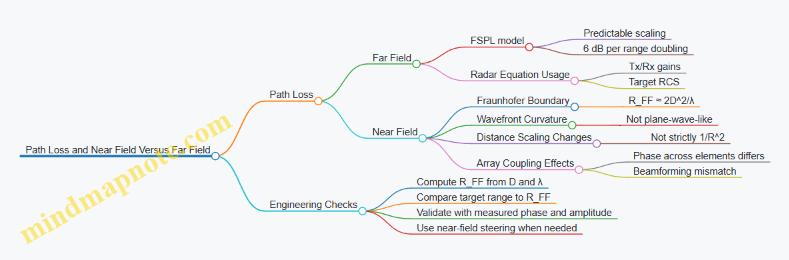
Example: Choosing the Correct Model in a Design Review
Assume a phased array with largest dimension \(D=15,\text{mm}\) at \(f=240,\text{GHz}\) (\(\lambda\approx 1.25,\text{mm}\)). Then \(R_{FF}\approx 2\cdot(0.015)^2/0.00125\approx 0.36,\text{m}\). If your radar must detect targets at 0.25 m, you should not rely on far-field steering vectors or expect FSPL-only scaling to match measurements.
A practical workflow is to:
- compute \(R_{FF}\),
- mark the near-field region for your operating ranges,
- and, for link budget sanity, treat near-field operation as a “model mismatch risk” that must be validated with phase-consistent measurements or a near-field propagation model.
Summary of What to Remember
Far-field path loss gives you clean, checkable scaling and a straightforward link budget. Near-field operation changes the geometry of phase and amplitude across the aperture, so the effective loss can look worse or behave differently than FSPL predicts. The fastest way to avoid surprises is to compute \(R_{FF}\) early and align your beamforming and path loss assumptions with the actual operating regime.
2.3 Multipath, Scattering, and Polarization Effects in Real Environments
Real THz and mmWave radar rarely see a clean line-of-sight (LOS) return. Instead, the receiver sees a sum of delayed, attenuated, and phase-shifted replicas created by reflections, scattering, and polarization changes. The practical goal is to predict how these effects reshape range cells, Doppler bins, and angle estimates—then design the RF front end and calibration so the damage is measurable and manageable.
Multipath Foundations and How It Shows Up in Radar
Multipath means multiple propagation paths arrive with different delays and phases. In a coherent radar, each path contributes a complex phasor to the same range bin if its delay falls within the waveform’s range resolution cell. If delays differ by more than the resolution, energy spreads across adjacent range bins.
A concrete example: suppose a target at 10.0 m produces a strong LOS echo, and a nearby wall produces a reflection that is effectively 0.3 m longer. With a 1.0 m range resolution, both echoes land in the same range cell and interfere. If the relative phase happens to be near 180°, the measured amplitude drops even though the target is present. If it is near 0°, the amplitude increases. This is why “range detection” can look inconsistent across repeated runs.
Scattering Mechanisms and Their RF Signatures
Scattering is the conversion of incident electromagnetic energy into many directions. In real environments, scattering strength depends on surface roughness relative to wavelength, object geometry, and material properties.
At THz, small geometric features can become electrically large, so scattering can be stronger and more directionally complex than at lower microwave bands. A metal edge can act like a specular reflector for some angles and like a diffuse scatterer for others. A rough surface can produce a cluster of weak returns with a wide angular spread.
Practical implication: scattering changes not only amplitude but also angular distribution. In a phased array, this can widen the apparent point spread function, raising sidelobe levels and increasing false alarms near strong reflectors.
Polarization Effects and Cross-Polar Returns
Polarization mismatch occurs when the transmitted polarization does not match the polarization of the received field after reflection or scattering. Even if the antenna polarization is fixed, reflections can rotate polarization depending on incidence angle and surface properties.
A simple example: transmit with vertical polarization. A reflection from a surface at a certain angle may return a component that is partially horizontal. If your receiver chain is sensitive primarily to vertical, the cross-polar component reduces measured power. In a dual-polar system, you would observe energy in both channels; in a single-polar system, it looks like fading.
Polarization also affects phase. The received complex field includes polarization-dependent phase shifts, so cross-polar components can interfere differently than co-polar components. That interference can shift the apparent phase center across channels, which matters for coherent beamforming.
Coherence, Phase Noise, and Multipath Interference
Multipath interference is coherent within the radar’s coherent processing interval. If the channel phase evolves due to motion, the interference pattern changes over time, producing fluctuations in detected amplitude and estimated Doppler.
Phase noise in the LO and oscillator distribution can compound this. When multiple paths arrive, each path’s contribution is multiplied by the same LO phase error, but the relative delay-to-phase mapping still differs across paths. The result is that multipath can make phase noise effects appear worse in angle and velocity estimation, because the effective signal is a mixture of phasors rather than a single tone.
Mind Map: Multipath, Scattering, and Polarization Effects
Example: Interpreting a “Good Range, Weird Angle” Return
Imagine a radar with a strong target at a known range, but the estimated angle drifts between frames. One explanation is multipath: a strong reflector near the array creates a secondary path with a different angle of arrival. If that secondary path is within the same range cell, it can pull the beamformed peak away from the true target direction.
Now add polarization: if the secondary reflector produces more cross-polar energy, the effective weighting across receive channels changes. That changes the relative phasor contributions across the array, so the beam peak can shift even when the target’s physical location is constant.
Example: A Simple Measurement Workflow for Real Environments
- Place a static target at a fixed position and record multiple coherent frames.
- Observe range cell amplitude stability; large fluctuations suggest multipath interference within the resolution cell.
- Compare angle estimates across frames; consistent range with varying angle points to angularly distinct multipath.
- If available, compare co-polar and cross-polar channels; a strong cross-polar component indicates polarization rotation that can bias coherent combining.
This section’s takeaway is practical: multipath, scattering, and polarization are not separate problems. They combine into a complex received field whose amplitude, phase, and angular content must be treated together when designing and validating THz/mmWave radar front ends.
2.4 Phase Noise Impact on Coherent Processing and Range Cells
Coherent radar processing assumes that the transmitted waveform and the receiver’s local oscillator (LO) maintain a stable phase relationship over the integration time. Phase noise breaks that assumption by turning a single “ideal” carrier into a cluster of nearby frequencies. In range processing, that frequency spreading shows up as range-cell smearing and elevated sidelobes; in Doppler processing, it can blur velocity estimates.
Phase Noise Basics That Matter for Range Cells
Phase noise is usually modeled as random phase fluctuations ϕ(t) added to the LO phase. If the LO is used to mix the received signal down, the residual phase error becomes part of the baseband signal. For coherent processing, the key quantity is how much the phase error changes during the time span that contributes to a range bin.
A practical way to connect phase noise to range cells is to look at the effective time-domain correlation. If the phase error is small and slowly varying, the coherent sum across samples stays constructive. If the phase error rotates significantly within the coherent integration window, the sum loses magnitude and spreads energy.
Where Range Processing Gets Hit
Range processing depends on the waveform type, but the mechanism is consistent: phase noise introduces an additional time-varying term that is not aligned with the assumed signal model.
For FMCW or chirp-based processing, the receiver beat frequency is mapped to range. Phase noise on the LO (and on the transmit chain, if it is not perfectly tracked) perturbs the instantaneous frequency, which perturbs the beat frequency. The result is a broadened peak in the range spectrum and a higher noise floor in adjacent cells.
For pulsed coherent processing with matched filtering, phase noise effectively reduces the matched-filter gain. The matched filter expects a specific phase evolution; phase noise adds mismatch, so the correlation peak drops and the sidelobe structure becomes less controlled.
Coherent Integration Loss in One Equation
A useful mental model is that coherent integration multiplies the ideal signal by a “coherence factor” that depends on phase error statistics. If the phase error over the integration time has variance σ², the expected coherent amplitude scales roughly like exp(-σ²/2). That single factor explains two common observations: (1) the main peak shrinks, and (2) the relative contribution of sidelobes and noise grows.
To make this concrete, suppose your system integrates for a time T and the LO phase noise produces a phase variance of σ² = 0.2 rad² over that interval. The coherence factor is exp(-0.1) ≈ 0.90, so you lose about 1 dB of coherent gain. If σ² rises to 1.0 rad², exp(-0.5) ≈ 0.61, which is about 4.3 dB loss. That loss directly reduces detection margin and makes range peaks less distinct.
Range Cell Smearing and Sidelobe Growth
Phase noise does not only reduce peak height; it redistributes energy. In frequency terms, phase noise broadens the carrier, which means the matched filter or FFT bin no longer captures all energy in one cell. In range terms, this appears as:
- Wider main lobes in the range profile.
- Higher sidelobes near the target cell.
- Increased apparent noise floor, especially when the processing uses narrow bins.
A simple example: imagine a target that would produce a clean single-cell peak with an ideal LO. With phase noise, the peak spreads across multiple bins. If your detection threshold is set based on noise-only cells, the smeared energy can push neighboring cells above threshold, increasing false alarms.
Practical Design Levers
- Reduce phase noise at the LO source: Lower phase noise reduces σ² over the integration window. The payoff is immediate in both peak height and sidelobe behavior.
- Shorten the coherent integration window when appropriate: If you can tolerate less integration gain, you reduce phase error accumulation. This is a trade with sensitivity.
- Use consistent phase tracking across channels: In arrays, channel-to-channel phase noise differences can create angle-dependent artifacts that look like range anomalies after beamforming.
- Choose processing windows that manage sidelobes: Windowing can’t fix coherence loss, but it can control how redistributed energy manifests across range bins.
Mind Map: Phase Noise to Range Cell Effects
Example: Estimating Coherent Gain Loss from Phase Variance
Assume a coherent integration time T where the LO phase noise leads to phase variance σ² = 0.5 rad². The expected coherent amplitude factor is exp(-0.25) ≈ 0.78. In dB, that is 20·log10(0.78) ≈ -2.1 dB. If your link budget had 6 dB margin, you now have about 3.9 dB margin before considering other non-idealities like gain compression or calibration errors.
Next, consider range sidelobes. If the peak drops by 2.1 dB while the noise floor rises due to energy spreading, the contrast between the target cell and nearby cells shrinks. That makes thresholding more sensitive to processing details such as window choice and bin width.
Example: Array Coherency and Range Artifacts
In a phased array, each channel’s LO phase noise may be correlated or uncorrelated depending on the architecture. If uncorrelated, beamforming weights that assume a stable phase relationship can partially cancel the desired signal in some directions. After range FFT or matched filtering, that cancellation can look like reduced peak amplitude and uneven sidelobe patterns across range cells. The fix is not “better range processing” but better coherency: common reference distribution, careful calibration, and phase noise-aware channel matching.
Summary of the Mechanism
Phase noise reduces coherent processing gain by breaking phase alignment over the integration window. It also redistributes energy across range bins by broadening the effective carrier spectrum and perturbing the signal model used by range processing. The combined result is lower peak amplitude, wider main lobes, and higher sidelobes or adjacent-cell energy, which directly affects detection thresholds and false alarm behavior.
2.5 Practical Calibration Strategies for Channel Measurement and Verification
Channel calibration is the part where you stop trusting “typical” and start trusting your actual hardware. In a phased array radar, you want each channel’s gain and phase to be known well enough that beamforming weights do what you think they do. The goal is not perfect truth; it’s repeatable truth under the same operating conditions.
Calibration Objectives and What “Good” Means
Start by separating two error sources:
- Channel-to-channel mismatch: one element’s phase is consistently offset from another, or one has slightly different gain.
- Time-varying drift: phase and gain change with temperature, LO behavior, or supply noise.
A practical target is to reduce residual phase error to a level that does not dominate your beamforming sidelobe and pointing accuracy. For example, if your array needs stable coherent summation, a few degrees of uncorrected phase error can noticeably smear the beam. Gain mismatch matters too, especially when you rely on coherent integration across many pulses.
Measurement Setup Foundations
Before any calibration run, lock down these basics:
- Define the reference plane: decide whether calibration values apply at the beamformer IC input, at the antenna feed, or at the RF connector. Your de-embedding choices follow this.
- Control the operating point: keep PA bias, LNA gain mode, and LO frequency settings fixed during the measurement series.
- Use consistent waveform conditions: if you calibrate with one chirp slope or modulation depth, don’t expect the same correction to hold for a different waveform unless you re-run the calibration.
A simple sanity check is to measure a single channel repeatedly. If its phase and gain wander more than your expected correction resolution, you are calibrating noise.
Gain and Phase Extraction from Channel Measurements
You typically estimate complex channel response as a function of frequency bin (for wideband) or as a single value (for narrowband). A common approach is to inject a known signal and measure the received complex response per channel.
- Narrowband example: inject a CW tone near the operating frequency. Measure I/Q at the receiver for each channel. Compute complex gain as \(H_k = I_k + jQ_k\). Normalize all channels to a chosen reference channel.
- Wideband example: transmit a known chirp or stepped tone set. For each frequency bin, compute the complex response per channel and derive correction weights \(C_k(f)\) so that \(H_k(f),C_k(f)\) matches the reference.
In both cases, you must handle phase wrapping and ensure the reference channel is stable. If the reference channel has its own drift, your “corrections” will chase a moving target.
Calibration Workflow That Actually Works
Use a repeatable sequence:
- Warm-up and settle: power the system and wait until temperature and bias conditions stabilize. Record the time you start calibration so you can repeat it later.
- Coarse alignment: run a quick measurement to estimate large offsets. This catches swapped cables, wrong channel mapping, or gross LO routing mistakes.
- Fine estimation: compute complex corrections per channel. For wideband, fit a smooth model across frequency if the hardware response is smooth; otherwise store per-bin corrections.
- Verification run: apply corrections and re-measure. Verification is where you prove the correction reduces mismatch, not just where you compute it.
A practical trick: do verification with a different signal condition than the one used for estimation. For instance, if you estimated using one tone frequency, verify using a nearby tone. This catches frequency-dependent errors you might otherwise miss.
Mind Map: Channel Calibration Strategy
Example: Two-Stage Calibration with a Simple CW Tone
Assume four channels. Pick channel 1 as reference.
- Measure complex responses \(H_1, H_2, H_3, H_4\) at the CW tone.
- Compute corrections \(C_k = H_1 / H_k\).
- Apply \(C_k\) in your beamforming weight computation.
- Verify by re-measuring \(H_k,C_k\). You should see the corrected channels align in phase and amplitude.
If channel 3 aligns in phase but not amplitude, your correction model is missing gain behavior (for example, you measured at one receiver gain setting and will run at another). If multiple channels show a common phase shift, your reference plane or LO distribution assumption is off.
Example: Wideband Calibration with Frequency Bins
For a chirp-based system, compute \(H_k(f_i)\) per bin \(f_i\). Then store \(C_k(f_i) = H_{ref}(f_i)/H_k(f_i)\).
Verification should check two things:
- Bin-to-bin consistency: corrected responses should track across frequency, not just at one bin.
- Beamforming impact: form a beam with corrected weights and compare pointing and sidelobe behavior against the uncorrected case.
If corrected beams still smear, the issue may be timing alignment rather than pure gain/phase. In that case, channel calibration values alone won’t fix the problem.
Practical Notes for Reliable Results
- Metadata matters: store calibration with the LO setting, receiver gain mode, and any bias configuration used.
- Don’t mix measurement modes: if you calibrate in one mode (e.g., different LNA gain or different IF filtering), re-calibrate for the other mode.
- Check channel mapping early: a swapped channel looks like a phase error until you compare physical routing.
A good calibration is one you can re-run and get the same correction behavior under the same conditions. That’s the difference between “we measured something” and “we can trust the array.”
3. Phased Array Architecture for Radar Beamforming IC Integration
3.1 Array Element Signal Chain Overview and Partitioning
An array element signal chain is the path from the radar’s coherent reference to the radiated wave, plus the return path from echoes back to the same coherent reference. Partitioning means you decide which functions live in the beamforming IC, which live in the RF front end, and which live in the baseband or digital domain. Done well, it keeps phase relationships stable, simplifies calibration, and prevents “mystery” gain or phase shifts from creeping in.
Core Partitioning Idea
Start by naming three reference points per channel:
- Reference clock and LO phase: the source of coherence.
- RF interface boundaries: where signals cross between ICs/modules.
- Digital sampling boundary: where ADC samples become coherent data.
A practical partitioning rule is to keep the number of boundaries small and make each boundary measurable. If you can’t measure it, you can’t calibrate it, and you’ll end up compensating with guesswork.
Transmit Path Signal Chain
A typical transmit chain per element looks like this:
- Beamforming IC baseband control generates the per-channel complex weights (amplitude and phase) and drives the waveform generation interface.
- DAC or modulator interface produces the transmit modulation signal.
- Upconversion shifts the signal to the desired radar band using mixers and local oscillators.
- PA drive and amplification boosts power while preserving phase as much as the device allows.
- Output filtering and matching shapes the spectrum and ensures the PA sees a stable load.
- Antenna feed and radiating element convert guided RF energy into free-space fields.
A concrete example: suppose you need a 77 GHz FMCW radar. The beamforming IC sets per-element phase so the array steers correctly. The LO at 77 GHz must be phase-coherent across channels; otherwise, steering errors show up as angle bias. The PA may add AM-to-PM conversion, so amplitude weights can subtly change phase. That’s why amplitude and phase calibration must be treated as linked, not independent.
Receive Path Signal Chain
The receive chain per element mirrors the transmit chain but with different constraints:
- Antenna and LNA input capture weak echoes with low added noise.
- Front-end filtering limits out-of-band interference and protects mixers.
- Mixer downconversion converts RF to an IF or baseband frequency.
- IF gain and filtering set the signal level for ADC without clipping.
- ADC sampling produces coherent samples aligned to the same reference.
Example: if one channel’s LNA gain drifts by 1 dB, the beamformer weights no longer match the assumed channel responses. Even if phase is perfect, the array’s effective pattern changes because coherent summation depends on both amplitude and phase. That’s why receive partitioning should include a plan for gain monitoring or periodic calibration.
Partitioning Boundaries That Matter
Not all boundaries are equal. Prioritize these:
- LO distribution boundary: phase noise and skew here directly affect coherent processing.
- Beamforming IC to RF boundary: any additional phase shift with temperature or supply variation must be characterized.
- RF to IF/baseband boundary: conversion gain variation changes dynamic range and affects detection thresholds.
A useful mental model is to treat each boundary as a “transfer function” that you can measure: (H(f, T, V)). Your job is to keep it stable or to measure it often enough that calibration stays valid.
Mind Map: Array Element Partitioning
Practical Example: One Channel from Weights to Radiated Beam
Imagine a single element channel in a 16-element array.
- The beamforming IC computes a complex weight \(w = a e^{j\phi}\) for the desired steering angle.
- The transmit modulation signal is generated and upconverted to the radar band.
- The PA amplifies the signal; if the PA’s phase shifts with output power, then changing \(a\) changes the effective phase.
- The antenna radiates the resulting field.
- On receive, the same element’s echo is amplified and downconverted.
- The ADC samples the result, and the beamformer applies the same \(w\) logic to coherently sum across elements.
If you partition the PA control and the beamforming weights without accounting for AM-to-PM behavior, the array will steer correctly at one power level and slightly miss at another. The fix is not magic; it’s measurement and calibration that ties amplitude control to phase correction.
Summary of What “Good Partitioning” Looks Like
Good partitioning makes coherence manageable, keeps boundaries measurable, and ensures that calibration targets the real transfer functions. When you can point to where phase and gain are set, where they drift, and where you can measure them, the rest of the system design becomes straightforward rather than mysterious.
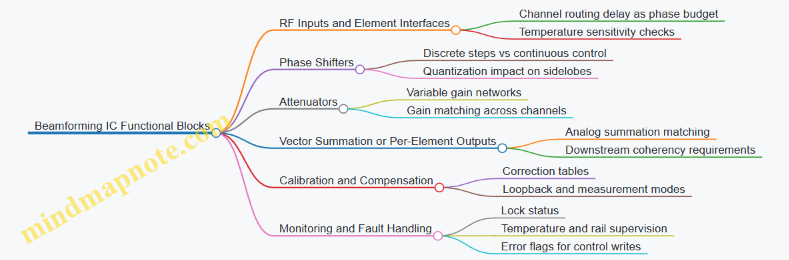
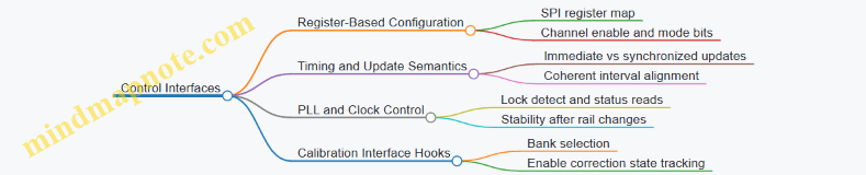
3.2 Beamforming IC Functional Blocks and Control Interfaces
A beamforming IC is the “traffic controller” between your RF front end and your digital radar processing. It decides how much each antenna element contributes, then applies phase and amplitude weights in a way that stays coherent across channels. To design and debug effectively, it helps to map the IC into functional blocks and then connect those blocks to the control interfaces you will actually use.
Functional Blocks from Signals to Weights
RF Inputs and Element Interfaces
Most beamforming ICs accept one RF input per channel (or per subarray), then route that signal through a controlled network. The key practical detail is that the IC must preserve phase relationships: any internal routing delay becomes part of your phase budget. A simple check is to measure relative phase between two channels at a fixed frequency before you start beamforming; if the phase offset changes with temperature, you will need calibration hooks.
Phase Shifters and Attenuators
Beamforming weights are typically implemented as a combination of phase shifting and amplitude control. Phase shifters may be implemented with switched transmission paths, vector modulators, or continuous-time control elements. Attenuators may be variable resistive networks or digitally controlled gain stages. The important engineering nuance is quantization: if phase steps are discrete, your beam sidelobes and null depth will reflect that. A concrete example: with 6-bit phase resolution over 360°, the step is 360/64 = 5.625°. If you instead have 3-bit resolution, the step becomes 45°. That difference shows up immediately in pattern measurements.
Vector Summation and Output Routing
Some ICs provide a summed output per beam, while others keep outputs per element and let the digital side do summation. If the IC sums analog signals, you must consider gain/phase matching across the summation network and the impact of output impedance on the next stage. If the IC outputs per element, you focus more on channel-to-channel coherency and the downstream ADC driver and clocking.
Calibration and Compensation Support
Many beamforming ICs include calibration memory, correction tables, or built-in loopback modes. Even when calibration is “optional,” you should treat it as required for repeatable results. A practical approach is to store per-channel phase and gain correction values derived from a measurement sweep, then apply them through the same control interface used for beam steering.
Status, Monitoring, and Fault Handling
Monitoring blocks may report lock status for internal PLLs, temperature sensors, supply rails, or error flags for control writes. These signals matter because beamforming errors often look like “mysterious” pattern distortion. For example, if one channel’s control register fails to update, you may see a lopsided beam that still roughly points correctly.
Control Interfaces and Their Practical Meaning
Register-Based Configuration
Most beamforming ICs are configured through a register map accessed via SPI or similar serial buses. The register map usually includes: channel enable bits, phase and gain settings, calibration memory selection, and mode control. A good habit is to write a known test pattern: set all channels to the same phase and amplitude, then verify that the RF outputs match expected relative levels.
Timing and Update Semantics
Control interfaces often support either immediate updates or synchronized updates. Synchronized updates are crucial when you change beam weights during a coherent processing interval. If updates are asynchronous, different channels may switch at slightly different times, creating transient phase errors. A simple example: if your radar updates weights every 10 µs, but the IC applies per-channel writes as they arrive over the bus, the last channel might lag by microseconds, which can smear coherent integration.
PLL and Clock Control Interfaces
If the IC contains internal frequency generation or phase-locked loops, it may expose lock detect pins or status registers. Even if you do not use internal generation, you still need to ensure that any internal timing references are stable. A practical check is to read lock status after power-up and after any supply rail changes, then correlate lock transitions with any observed pattern changes.
Calibration Interface Hooks
Calibration may be controlled by selecting a calibration bank, enabling correction, or triggering a measurement mode. The key is to keep calibration state explicit in your system software. If you switch between “raw” and “corrected” modes without tracking it, you will waste time chasing a pattern that looks like a hardware issue but is actually a configuration mismatch.
Mind Maps: Beamforming IC Functional Blocks and Control Interfaces
Example: A Systematic Bring-Up Sequence
- Set a baseline weight: program all channels to the same phase and amplitude. Confirm relative phase stability by measuring two channels at a fixed frequency.
- Verify quantization behavior: step phase through a small set of codes and record the resulting phase shift. If the phase steps are not monotonic, you likely have a control update timing issue.
- Test synchronized updates: change weights using the IC’s update mechanism (if available). Compare beam pointing stability with and without synchronized updates.
- Enable calibration corrections: switch to a corrected calibration bank and re-measure beam symmetry. If symmetry improves, your correction path is wired correctly; if it worsens, you may have channel indexing swapped.
- Check monitoring signals: during the same tests, log lock status and fault flags. If a channel shows a persistent fault, treat it as a configuration or power integrity problem before touching RF tuning.
This block-and-interface view keeps the design grounded: you know where phase and gain are created, how they are controlled, and what signals tell you whether the IC is behaving like the registers say it should.
3.3 Beam Steering, Beam Squint, and Quantized Phase Effects
Beam steering in a phased array is mostly about controlling relative phase across elements. In an ideal world, you pick a steering angle, compute the phase for each element, and the beam points there for every frequency in your waveform. In the real world, the beam can drift with frequency (beam squint) and the phase you request can’t always be set continuously (quantized phase). Both effects are predictable, measurable, and manageable.
Beam Steering Basics with a Frequency Reference
Assume a linear array with element spacing d and element index n. For a chosen steering angle \(\theta_0\), the required phase progression across elements at a reference frequency \(f_0\) is
\[\Delta\phi_0 = -2\pi,\frac{d}{\lambda_0},\sin(\theta_0)\]
where \(\lambda_0 = c/f_0\). A practical implementation uses a beamforming IC that applies per-channel phase weights. A simple mental check: if \(\theta_0 = 0\), then \(\sin(\theta_0)=0\) and all elements get the same phase, so the beam is broadside.
Example: A 16-element array with d = 0.5\(\lambda_0\) steers to \(\theta_0 = 30^\circ\). Then \(\Delta\phi_0 = -2\pi\cdot 0.5\cdot \sin(30^\circ)= -\pi/2\) per element. Element n uses phase \(\phi_n = n\Delta\phi_0\) (mod 2\(\pi\)).
Beam Squint from Frequency-Dependent Phase Progression
A steering phase set for \(f_0\) is proportional to \(d/\lambda\), so it changes with frequency. When the array transmits or receives a wideband signal, each frequency component experiences a different effective steering angle.
At frequency f, the phase progression becomes
\[\Delta\phi(f) = -2\pi,\frac{d}{\lambda(f)},\sin(\theta_0) = -2\pi,\frac{d f}{c},\sin(\theta_0)\]
But the beamforming hardware still applies the phase pattern computed for \(f_0\). The result is an effective steering angle \(\theta(f)\) that satisfies
\[\sin(\theta(f)) = \frac{f_0}{f},\sin(\theta_0)\]
So higher frequencies steer closer to broadside (smaller \(\sin\) term), and lower frequencies steer farther.
Example: Let \(\theta_0=30^\circ\) so \(\sin(\theta_0)=0.5\). If the signal spans \(f=f_0\pm 10\%\):
- At \(f=1.1f_0\): \(\sin(\theta)=0.5/1.1\approx 0.455\Rightarrow \theta\approx 27.1^\circ\)
- At \(f=0.9f_0\): \(\sin(\theta)=0.5/0.9\approx 0.556\Rightarrow \theta\approx 33.8^\circ\)
That spread matters because radar angle estimation often assumes a single steering direction per processing bin.
Quantized Phase Effects from Discrete Tuning Steps
Beamforming ICs typically implement phase weights with finite resolution, such as Q bits. The phase step is \(\Delta\phi_q = 2\pi/2^Q\). Instead of applying the ideal \(\phi_n\), the system rounds to the nearest quantized value, creating phase error \(e_n\).
A useful way to reason is to treat quantization as adding a bounded error per element. If the errors are roughly uncorrelated across elements, the main lobe remains near the intended angle but sidelobes rise and the peak gain drops slightly.
Example: With Q = 6 bits, \(\Delta\phi_q = 2\pi/64\approx 5.625^\circ\). If the ideal per-element phase progression is \(-90^\circ\), the programmed value might be \(-90\pm 2.8^\circ\) depending on rounding. Across 16 elements, this can measurably reduce coherent addition at the beam peak.
Quantization also interacts with beam squint: at off-center frequencies, the ideal phase progression is already “wrong,” and quantization adds another layer of mismatch.
Mind Map: Beam Steering, Beam Squint, and Quantized Phase
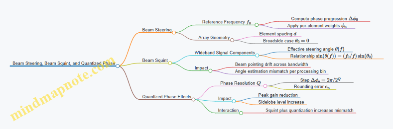
Practical Design Practices with Concrete Checks
-
Compute squint over your actual bandwidth. Use \(\sin(\theta(f)) = (f_0/f)\sin(\theta_0)\) at the band edges and compare the angle spread to your system’s angular resolution. If the spread is larger than the resolution, expect peak loss or biased angle estimates.
-
Choose element spacing with squint in mind. Larger d increases phase sensitivity to frequency, which typically worsens squint. A quick check is to keep d near the conventional fraction of \(\lambda_0\) unless you have a deliberate reason.
-
Quantization budgeting. If your beamforming IC has Q bits, estimate the maximum phase error as \(\pm\Delta\phi_q/2\). Then verify with a simple array factor simulation or measurement sweep: look for main-lobe peak reduction and sidelobe rise at the steering angle.
-
Validate with a two-step measurement. First, measure beam pointing at a narrowband tone near \(f_0\) to confirm steering correctness. Second, repeat at band-edge tones to quantify squint directly. Finally, compare results between adjacent quantized settings if the IC supports it.
Example: Putting It Together for a Small Radar Array
Suppose you steer to \(30^\circ\) with a 16-element array at \(f_0\), your waveform spans \(\pm 10\%\), and your phase resolution is Q = 6 bits. From the squint calculation, the beam peak moves roughly from \(27.1^\circ\) to \(33.8^\circ\). From quantization, you expect bounded phase errors of about \(\pm 2.8^\circ\) in phase terms per element. Together, you should anticipate a noticeable drop in coherent gain at the intended angle when processing the full band, and a sidelobe pattern that is slightly less controlled than the ideal continuous-phase case. The fix is not magic: it’s either narrower bandwidth, better phase resolution, or a processing approach that accounts for frequency-dependent pointing.
3.4 Beam Pattern Measurement and Verification Methods
Beam pattern measurement is where theory meets reality: you can compute array factors all day, but the hardware decides the actual phase, amplitude, and sidelobes. This section lays out a systematic path from basic definitions to repeatable verification workflows for phased array radar front ends.
Beam Pattern Basics and What You Actually Measure
A phased array beam pattern describes how radiated (or received) power varies with angle. In practice you measure either:
- Transmit pattern: how much power leaves the array versus angle.
- Receive pattern: how much signal the array captures versus angle.
- Monostatic radar pattern: the combined effect of transmit and receive chains, often treated as a product of both.
A useful starting point is the array factor idea: ideal steering sets relative phases across elements, producing a main lobe at the commanded angle and sidelobes elsewhere. Real measurements add errors from element gain variation, phase quantization, mutual coupling, and frequency-dependent behavior.
Concrete example: if you command 30° steering on a 16-element array, the ideal main lobe might land exactly at 30°. In measurement you might see the peak at 29.2° because the effective phase slope across the array is slightly off.
Measurement Setups and Their Tradeoffs
You have three common measurement approaches, each with different sources of error.
-
Over-the-air (OTA) angle sweep
- Place a known RF source or reflector at varying angles.
- Measure received power (or transmitted power) at each angle.
- Best for end-to-end verification of beamforming weights and RF chain behavior.
-
Near-field scanning with planar transforms
- Scan the field close to the array.
- Use near-to-far field transformation to infer far-field pattern.
- Useful when far-field ranges are impractical.
-
Channel-based pattern reconstruction
- Measure per-channel gain and phase using calibration tones.
- Reconstruct the expected pattern numerically.
- Fast and repeatable, but it assumes the model captures coupling and element radiation correctly.
A practical rule: use OTA to validate the reconstruction model, then rely on reconstruction for routine checks.
Instrumentation and Signal Conditioning
To compare measurements across runs, control the signal chain.
- Use coherent excitation when possible. For receive pattern, coherent tones help separate phase-related effects from noise.
- Set a stable reference level. Record absolute power only if your calibration supports it; otherwise focus on normalized patterns (main-lobe and sidelobe levels).
- Control polarization. If your array is linearly polarized, rotate the test source polarization to match; otherwise you measure polarization mismatch instead of beamforming.
Concrete example: if you normalize each angle sweep to the peak, you can compare sidelobe levels even when absolute power drifts due to temperature.
Step-by-Step OTA Angle Sweep Workflow
A repeatable workflow reduces “mystery differences” between labs.
-
Select a test frequency or narrow band
- For phased arrays, beam direction can shift with frequency (beam squint). Keep the sweep narrow if you want a single-angle result.
-
Choose steering angles and step size
- Use a step small enough to capture the main lobe shape. A common starting point is 0.2–0.5° for narrow beams, larger for wider beams.
-
Apply beamforming weights and verify channel settings
- Confirm phase register values, gain modes, and any calibration offsets are loaded correctly.
-
Perform the angle sweep
- Record received power versus angle for each steering command.
-
Normalize and extract metrics
- Compute main-lobe peak angle, 3 dB beamwidth, peak sidelobe level (PSL), and integrated sidelobe level (ISL) if needed.
-
Repeat for multiple runs
- Repeat at least twice to estimate repeatability. If results shift, suspect mechanical alignment, temperature, or LO coherence.
Near-Field Scanning and Transformation Checks
Near-field methods require careful geometry.
- Ensure correct scan plane relative to the array phase center.
- Use sufficient spatial sampling so the transform does not alias the field.
- Verify transformation sanity by checking that the reconstructed pattern matches a known steering case.
Concrete example: if the reconstructed main lobe appears consistently shifted by the same angle for every steering command, the phase center reference or scan plane alignment is likely off.
Channel-Based Reconstruction Verification
Reconstruction is powerful when you can measure the array’s effective element responses.
-
Measure complex channel responses
- For each element, estimate gain and phase at the test frequency.
-
Build the steering model
- Combine measured element responses with commanded weights.
-
Compute the expected pattern
- Use the array geometry and element radiation model (even a simple model can work for first-pass checks).
-
Compare to OTA
- Match peak angle and sidelobe structure. If sidelobes disagree but peak angle matches, suspect amplitude taper errors or coupling.
Error Sources and How to Diagnose Them
When patterns don’t match, the mismatch usually points to a specific class of error.
- Peak angle error: often phase slope error, timing skew, or LO distribution phase offsets.
- Sidelobe level error: often amplitude imbalance, quantized phase, or incorrect taper weights.
- Pattern asymmetry: often element-to-element phase errors that are not linear with index, or mechanical misalignment.
- Frequency-dependent beam shift: beam squint from phase-to-frequency scaling.
A quick diagnostic: if you re-run the same steering command at a second frequency and the peak shifts more than expected, focus on frequency-dependent phase behavior in the RF chain.
Mind Map: Beam Pattern Measurement and Verification
Example: Verifying a 16-Element Steered Beam
Command steering to 0°, 15°, and 30° at a single test frequency. For each command, run an OTA angle sweep and normalize each curve to its own peak. Extract peak angle and PSL.
- If 0° peak lands at 0.3° but 15° and 30° are similarly shifted, the phase slope is consistently biased.
- If peak angles match but PSL is higher than expected, the amplitude taper or gain calibration likely differs from the model.
- If asymmetry appears only at off-boresight angles, check mechanical alignment and polarization matching before chasing deeper RF causes.
This workflow turns “the pattern looks off” into a small set of measurable hypotheses you can test quickly.
3.5 Practical System Partitioning Between RF, IF, and Digital Processing
A good partitioning plan answers three questions early: what must be coherent across channels, what must be linear enough to preserve modulation and phase, and what can tolerate latency or quantization. In a THz/mmWave phased-array radar, the RF, IF, and digital domains each have different “failure modes,” so you want boundaries that match those modes.
RF Domain Responsibilities
The RF domain owns everything that touches the carrier: generation, distribution, switching, amplification, and the analog phase relationships that beamforming depends on. In practice, RF should handle:
- Coherent frequency generation and distribution so all channels share a stable phase reference.
- Transmit shaping at the analog level such as filtering, image rejection, and power control.
- Receive front-end gain and filtering that set the noise figure and protect later stages from overload.
- Phase-critical analog paths where component tolerances and routing matter.
A practical rule: if a signal’s phase must be consistent across elements for coherent processing, treat that path as RF even if it feels “almost digital.” For example, a variable phase shifter implemented with an analog control voltage belongs to RF because its settling time and nonlinearity can create phase errors that look like target motion.
IF Domain Responsibilities
The IF domain is the analog “middle ground” where you translate the problem into something the ADC can handle. IF typically owns:
- Downconversion and anti-alias filtering with predictable group delay.
- IF gain staging to use ADC dynamic range efficiently.
- Analog calibration hooks such as controllable attenuators or test tones.
A useful way to think about IF is “make the ADC boring.” If the IF chain produces stable amplitude and phase over temperature and time, digital can focus on coherent integration and detection.
Concrete example: suppose your ADC full-scale is 0 dBFS and your strongest expected return is 20 dB below it. You can set IF gain so typical signals sit around -10 to -6 dBFS, leaving headroom for clutter and interference. If you instead rely on digital scaling, you risk clipping during bursts and you lose phase linearity when the analog chain saturates.
Digital Domain Responsibilities
Digital processing owns everything that benefits from repeatability and algorithmic flexibility:
- Beamforming weights application and coherent summation.
- Range-Doppler processing such as FFTs and windowing.
- Detection logic including thresholding and clutter suppression.
- Calibration application for per-channel gain and phase corrections.
A practical boundary: digital should correct for slow mismatches (gain/phase offsets, static delays), while RF/IF should prevent fast distortions (clipping, excessive phase noise, unstable group delay). If you try to fix fast analog distortion digitally, you often end up correcting the wrong thing.
Mind Map: Partitioning Logic
Example: Choosing Where a Function Lives
Consider a per-channel phase calibration step. If you implement it by adjusting an analog phase shifter, you must ensure the phase shifter’s control path is stable and repeatable; otherwise, you inject additional uncertainty. If you implement it digitally by applying a complex weight, you assume the analog chain preserves phase linearly over the measurement window.
A practical approach is hybrid: use RF/IF to keep the chain within linear operation and stable group delay, then use digital to apply per-channel complex correction. This keeps the calibration from fighting analog non-idealities.
Example: Gain Staging and Anti-Alias Filtering
Assume a receive chain where the LNA output can vary by 30 dB depending on scene reflectivity. If you set IF gain once and never revisit it, you either waste ADC range on quiet scenes or clip on strong returns. A practical partitioning is to keep the IF gain strategy simple and bounded—use analog gain control or switched gain steps with known settling—then let digital handle fine scaling for display and detection.
In the same spirit, anti-alias filtering should be designed so its passband ripple and group delay are stable across the operating temperature range. If the filter’s delay varies unpredictably, coherent summation across channels suffers even when amplitude looks fine.
Verification Checklist for the Boundaries
- RF coherence check: measure relative phase across channels under the same LO conditions.
- IF linearity check: confirm no clipping in the ADC for the expected strongest returns.
- IF timing check: verify group delay stability so coherent processing doesn’t smear.
- Digital calibration check: apply gain/phase correction and confirm improvement in beam peak sharpness.
- End-to-end sanity check: run a loopback or controlled test signal and verify that the partitioning assumptions match reality.
4. RF Front-End Design for mmWave and THz Transmitters
4.1 Transmit Chain Topologies for Radar Waveforms
A radar transmit chain is easiest to reason about when you separate three jobs: (1) create a coherent carrier or LO, (2) generate the radar modulation waveform, and (3) deliver that waveform to the antenna with the right power, phase stability, and spectral cleanliness. Different transmit chain topologies mainly trade off where modulation happens, how coherence is preserved, and how much filtering and linearization you must do.
Foundational Building Blocks
Most radar transmitters can be mapped to these blocks:
- Coherent frequency source: a synthesizer or reference-driven oscillator that defines the carrier and timing.
- Modulation stage: produces the radar waveform (FM, phase-coded, chirped, pulse-shaped, or OFDM-like) by controlling phase, frequency, or amplitude.
- Upconversion: moves the waveform to the desired RF/THz band.
- Power amplification: raises power to the antenna level, often with GaN PAs.
- Filtering and spurious control: suppresses unwanted products from mixers, harmonics, and PA nonlinearity.
A practical rule: if your waveform requires tight phase coherence across pulses or channels, you want modulation to be as close as possible to the coherent source, or you must compensate phase changes introduced later.
Topology 1: Direct RF Modulation with Coherent Source
In this topology, the coherent source is modulated directly (or via a small-signal modulator) before power amplification. The chain looks like: coherent synthesizer → modulation control → driver amplifier → PA → output filtering.
When it fits well: phase-coded or frequency-stepped waveforms where you can tolerate the modulator’s bandwidth limits.
Easy example: Suppose you need 1 µs pulses with phase codes that change every pulse. You can generate the carrier at the radar center frequency, apply phase changes through the synthesizer control path, then amplify. Because the phase changes occur before the PA, the PA mainly adds amplitude gain and some phase shift that you can calibrate once per operating point.
Key design checks:
- Modulator control latency must be stable relative to pulse timing.
- PA gain compression must be managed so amplitude variations do not corrupt coherent processing.
- Output filtering must handle the modulator’s spurious sidebands.
Topology 2: IQ Modulation Upconversion Then PA
Here, you generate the waveform as an I/Q baseband (or low IF) signal, then upconvert using an IQ mixer to RF, followed by amplification. Chain: coherent reference → I/Q generation → IQ upconversion → driver → PA → filtering.
When it fits well: waveforms with controlled amplitude and phase, including pulse shaping and complex modulation.
Easy example: For a chirp-like waveform, you can synthesize the instantaneous frequency by controlling the I/Q phase trajectory. The IQ path lets you shape the envelope to reduce spectral splatter, which can ease filtering requirements after the PA.
Key design checks:
- IQ imbalance creates image leakage; you must ensure sufficient image rejection via calibration or careful mixer matching.
- LO feedthrough and DC offsets can create spurs; you need filtering and bias control.
- The PA sees a modulated RF signal; linearization may be required if you demand strict sidelobe limits.
Topology 3: IF Modulation with Later Upconversion
This topology performs modulation at an intermediate frequency, then upconverts once to the final RF/THz band. Chain: coherent LO → IF modulation generator → IF-to-RF upconversion → PA → filtering.
When it fits well: when baseband generation is inconvenient at very high frequencies, but you still want more control than direct RF modulation.
Easy example: If your radar needs a wideband chirp but your direct RF modulator bandwidth is limited, you can generate the chirp at IF, then translate it up. The translation preserves the chirp’s phase evolution if the LO is coherent and stable.
Key design checks:
- The upconversion stage adds phase noise from the LO; you must budget it against coherent integration needs.
- Image and mirror products depend on IF frequency placement; filtering must be designed accordingly.
Topology 4: Pulse Modulation at the PA Stage
Instead of shaping the waveform early, you keep the carrier mostly continuous and gate or modulate the PA drive to create pulses. Chain: coherent carrier → PA with envelope/pulse control → output filtering.
When it fits well: simple pulsed radars where phase coding is minimal or where timing is the dominant requirement.
Easy example: For a basic pulsed radar, you can switch the PA on for a fixed pulse width. The waveform is then mostly determined by the PA’s turn-on/off dynamics.
Key design checks:
- PA switching transients create spectral splatter; you may need a controlled ramp rather than a hard gate.
- Phase during the first part of the pulse can drift due to bias settling; you may need to discard early samples or calibrate.
Mind Map: Transmit Chain Topologies
Practical Selection Workflow
- Start with waveform type: phase-coded, chirped, or amplitude-shaped signals determine whether you need IQ control, IF modulation, or simple gating.
- Place modulation to match your coherence needs: if coherent processing is sensitive, prefer modulation earlier in the chain or ensure later stages are calibrated.
- Budget linearity where it matters: if the PA must handle complex modulation with tight sidelobe limits, plan for linearization and verify with the actual modulation, not a sine wave.
- Design filtering around real spurs: mixers and switching create predictable products; PA nonlinearity creates harmonics and intermodulation that your filters must suppress.
Integrated Example: Choosing Between Two Options
If you need a chirp with controlled sidelobes, IQ upconversion often helps because you can shape the envelope and manage spectral regrowth before the PA. If your system can only generate the chirp at IF due to hardware constraints, IF modulation with later upconversion preserves the chirp’s phase evolution as long as the LO is coherent and you include image rejection in the RF stage. In both cases, the final confirmation is the same: measure the transmitted spectrum and phase behavior using the exact waveform you intend to transmit, then verify that the PA operates in a region where your sidelobe and coherence targets remain satisfied.
4.2 Frequency Generation and Distribution for Coherent Operation
Coherent radar depends on having a stable, well-defined phase relationship between the transmit waveform and every receive channel. Frequency generation provides the “what frequency,” while distribution provides the “how consistently that frequency is delivered.” The goal is not just low phase noise at one point, but controlled phase noise, deterministic delay, and manageable spurs across the whole RF front end.
Coherent Requirements That Drive the Architecture
Start with three practical requirements:
- Phase continuity across chirps or pulses. If the radar uses coherent processing, the local oscillator (LO) must not introduce random phase jumps between coherent intervals.
- Channel-to-channel phase alignment. Beamforming needs relative phase accuracy between array elements; absolute phase can be calibrated out, but relative phase cannot be left to chance.
- Spur and leakage control. Any unwanted tones from synthesizers, dividers, or distribution paths can mix into the receiver band and create false detections.
A simple way to reason about this is to treat the LO path as a chain of phase contributions: synthesizer phase noise + distribution phase noise + conversion chain noise. Coherence fails when the combined phase error becomes large compared to the phase tolerance implied by your angle resolution and integration time.
Frequency Generation Options and Their Tradeoffs
A typical coherent chain begins with a reference oscillator, then uses a phase-locked loop (PLL) or direct digital synthesis (DDS) to create the radar carrier.
- Reference and synthesizer. A low-noise reference (often crystal-based) feeds a PLL. The PLL multiplies frequency, shaping phase noise and adding reference spurs at predictable offsets.
- Direct generation versus LO multiplication. Generating the exact carrier frequency directly can reduce multiplication stages, but may require higher loop bandwidth or more complex tuning. Multiplication is common because it keeps the PLL operating in a comfortable range.
- Common LO versus per-channel synthesis. For coherent arrays, a single common LO distributed to all channels usually beats independent synthesizers. Independent sources add uncorrelated phase noise and complicate calibration.
Distribution Topologies for Coherent Arrays
Distribution is where many designs accidentally lose coherence.
1. Central LO with fan-out. One LO source drives a power splitter network feeding each channel.
- Best for coherence because all channels share the same source.
- Requires careful equalization of path lengths and control of splitter-induced amplitude/phase differences.
2. Central LO with per-channel phase trimming. After fan-out, each channel includes a controllable phase element.
- Useful when routing lengths differ or when packaging introduces fixed phase offsets.
- Keep the trimming range and resolution consistent with the calibration strategy.
3. Local regeneration. Each module regenerates the LO using a local PLL locked to the common reference.
- This can reduce distribution loss and improve robustness.
- Coherence depends on how well the regenerated LOs preserve relative phase; you still need a calibration plan.
Phase Noise and Delay: What Actually Matters
Two different “imperfections” show up in coherent radar:
- Random phase noise. This broadens the effective tone and reduces coherent integration gain. It is often specified as phase noise in dBc/Hz at offsets from the carrier.
- Deterministic delay mismatch. If channel paths differ by a fixed time delay, the phase offset is constant and calibratable. If delays vary with temperature or motion, the offset becomes time-varying and degrades beamforming.
A practical design habit is to separate these in your thinking: treat fixed mismatch as calibration data, and treat variable mismatch as a stability problem.
Practical Distribution Design Steps
- Define the LO frequency plan. Decide whether the LO is used directly at the carrier or as an intermediate LO for mixing. The frequency plan determines which spurs can land in-band.
- Equalize electrical lengths. Match trace lengths, cable lengths, and connector types across channels. If perfect matching is impossible, measure and calibrate the residual.
- Control distribution loss. Use amplifiers or low-loss components so that receiver mixers see consistent LO power. Unequal LO power can change conversion gain and effective phase response.
- Manage reflections and isolation. Fan-out networks can create standing waves that convert small impedance changes into phase ripple. Terminate properly and isolate sensitive nodes.
- Keep the LO clean at the receiver. Place filtering or limiting where appropriate to prevent distribution spurs from propagating into the mixer.
Example: Coherent LO for a Four-Channel mmWave Receiver
Assume a common LO at 60 GHz distributed to four receiver channels.
- Use a central splitter network so all channels share the same source.
- Route each channel with matched lengths; if channel C is 2 mm longer than channel A, the fixed phase offset at 60 GHz is approximately:
- wavelength λ ≈ c/f ≈ 5 mm
- phase offset ≈ 360° × (2 mm / 5 mm) ≈ 144°
- That offset is constant, so you can calibrate it during system bring-up. The real risk is if the 2 mm effective difference changes with temperature due to different materials or mechanical stress.
Now consider phase noise: if the LO phase noise causes an rms phase error that grows with integration time, coherent summation loses gain. Your job is to ensure the LO phase noise level is low enough that the coherent processing gain meets the radar requirement.
Mind Map: Frequency Generation and Distribution for Coherent Operation
Example: A Simple Coherence Check Using Measured Phase
During bring-up, measure relative phase between channels using a tone at the receiver IF or baseband after downconversion. If the relative phase drifts significantly with temperature while LO power remains stable, the issue is likely distribution variability (cables, connectors, or unequal thermal paths). If relative phase is stable but beamforming performance is still off, the problem is more likely in calibration mapping or in channel-specific conversion chain phase behavior.
4.3 Upconversion, Filtering, and Image Rejection Techniques
Upconversion moves a radar waveform from an easier-to-generate frequency (often baseband or an IF) to the transmit RF band. In a coherent radar, the upconversion chain must preserve phase relationships across channels, because beamforming and coherent processing care about small timing and phase errors. The practical goal is simple: generate the desired sideband with enough suppression of the unwanted image, while keeping gain, phase, and distortion predictable.
Foundational Signal Paths from Baseband to RF
A common architecture starts with a complex baseband signal I(t) + jQ(t). Ideally, the modulator maps I and Q to a single RF sideband around a local oscillator (LO) frequency f_LO. If you instead use a real-only path, you effectively create both sidebands, and the “image” becomes a real problem rather than a theoretical nuisance.
A useful mental model is:
- Desired RF component sits at f_LO + f_IF (upper sideband) or f_LO − f_IF (lower sideband).
- Image component sits at the opposite side of the LO, at f_LO ∓ f_IF.
If the image falls into a region where your antenna, filters, or subsequent stages respond, it can mix back into the receiver or radiate directly, degrading range sidelobes and clutter rejection.
Upconversion Methods and Their Sideband Behavior
Single-sideband (SSB) generation is the cleanest approach when you can implement it. IQ modulation with proper amplitude and phase balance can produce near-SSB output, but it is only as good as the I/Q mismatch.
Double-sideband (DSB) generation is simpler but relies on filtering to suppress the unwanted sideband. In many radar transmitters, you accept some DSB and then use bandpass filtering plus system-level isolation.
A practical rule: if you can afford an IQ modulator and you can calibrate I/Q imbalance, you usually get better image suppression than “filter-only” approaches at the same cost.
Filtering Strategy from IF to RF
Filtering has two jobs: remove spectral images created by modulation and limit out-of-band emissions. The chain typically uses:
- Pre-filtering at IF or baseband to constrain the spectrum before modulation.
- Reconstruction or bandpass filtering at RF to select the desired sideband.
- Optional post-filtering for spurious cleanup and to protect later stages.
At THz and mmWave, filter selectivity is limited by component Q and packaging parasitics, so you design with realistic stopband attenuation. A good engineering habit is to treat filter attenuation as a budget item, not a guarantee.
Image Rejection with IQ Modulation and Calibration
Image rejection in an IQ upconverter depends on matching:
- Gain match between I and Q paths
- Phase match between I and Q paths
- LO feedthrough symmetry
When I and Q are mismatched, the “suppressed” sideband leaks back in. The leakage level can be estimated from mismatch. For example, a small phase error θ and gain error g produce finite image rejection; even a few degrees can matter when you need tens of dB of suppression.
A systematic calibration approach is:
- Inject a known tone at the IF (complex baseband).
- Measure the RF spectrum around f_LO.
- Adjust I/Q gain and phase to minimize the unwanted sideband.
- Repeat across the operating temperature range if the system is sensitive.
This is not magic; it’s just turning mismatch into a measurable parameter.
Practical Example: Choosing Between SSB and DSB + Filters
Suppose you transmit an IF-centered waveform at f_IF = 1.5 GHz with f_LO = 90 GHz. The desired sideband is at 91.5 GHz and the image is at 88.5 GHz.
- If your RF bandpass filter has only 25 dB stopband attenuation at 88.5 GHz, then the image level may still be significant, especially if your modulator is not near-ideal.
- If you implement IQ modulation targeting SSB and calibrate I/Q mismatch to achieve, say, 35–40 dB image suppression, the filter can be less aggressive while still meeting spectral mask.
The best choice depends on what you can control: modulator mismatch, filter stopband, and how much image energy the antenna and system can tolerate.
Mind Map: Upconversion, Filtering, and Image Rejection
Example: Quick Image-Rejection Check Using a Tone Sweep
Generate a single complex tone at the IF and sweep its frequency across the intended IF bandwidth. For each tone, measure the RF spectrum at both sidebands around f_LO. A good system shows:
- The desired sideband amplitude follows the expected modulation response.
- The image sideband stays suppressed with a relatively flat leakage trend across the IF range.
If the image suppression degrades at the band edges, it often points to frequency-dependent I/Q imbalance or imperfect filtering before the modulator. Fixing it usually means adjusting calibration frequency points or improving the IF filtering and matching networks.
4.4 Power Amplifier Drive Requirements and Gain Control Loops
A radar transmitter PA rarely behaves like an ideal gain block. Drive requirements and gain control loops exist to keep output power stable while the rest of the system stays coherent. The key is to treat “gain control” as a closed-loop system with measurable signals, defined bandwidth, and explicit limits.
Drive Requirements from Waveform to Output Power
Start with the waveform you must transmit: duty cycle, modulation type, and peak-to-average ratio. Convert that into a required PA output power profile, then work backwards to the drive level.
-
Define output power targets
- Pick a minimum output power at the worst-case operating point (temperature, supply tolerance, aging).
- Add headroom for calibration error and component tolerances.
- Example: If the radar needs 20 dBm average at the antenna port and your PA efficiency drops at high temperature, you may target 21–22 dBm at the PA output before losses.
-
Account for RF path losses
- Include losses from beamforming IC output, interconnects, filters, and matching networks.
- Example: If the PA input is 1 dB lower than the beamformer output due to a filter plus routing loss, you must raise the drive by that 1 dB to hit the same PA input power.
-
Translate output power to required input drive
- Use measured PA gain curves: output power vs input power at representative conditions.
- Identify the region you will operate in: linear region for modulation fidelity, or saturated region for efficiency.
- Example: If 0 dBm drive yields 25 dBm output at room temperature but only 23 dBm at high temperature, your gain control must compensate by raising drive by ~2 dB under those conditions.
-
Respect maximum drive and linearity constraints
- Ensure the drive does not exceed limits that cause excessive distortion, compression, or reliability stress.
- Example: If the PA’s input network begins to reflect strongly above a certain drive level, the loop may “work” but the output spectrum may fail mask requirements.
Gain Control Loop Architecture
A practical gain control loop needs three things: a sensing path, an actuator, and a control law that doesn’t fight the radar waveform.
- Sensing path: detect output power (or a proxy) with a detector diode, directional coupler, or internal monitor.
- Actuator: adjust PA drive via a variable gain stage, DAC-controlled attenuator, or bias control that changes gain.
- Control law: typically PI or PID with anti-windup and rate limiting.
Mind Map: Gain Control Loop Building Blocks
Choosing Loop Bandwidth Without Breaking the Modulation
If the loop reacts too quickly, it will treat waveform variations as “error” and modulate the gain, creating amplitude ripple and spectral artifacts. If it reacts too slowly, it will miss thermal drift and output power will wander.
A good starting point is to separate timescales:
- Fast timescale: waveform envelope and detector ripple.
- Slow timescale: temperature and supply drift.
Example workflow:
- Measure detector output during a representative transmit burst with the loop open.
- Identify the dominant ripple frequency from the envelope and detector dynamics.
- Set loop bandwidth well below that ripple so the loop averages over it.
Actuator Options and Their Tradeoffs
-
Variable attenuation or VGA gain
- Pros: typically preserves PA bias and can keep distortion behavior consistent.
- Cons: adds control range limits and may affect noise figure at the PA input.
-
Bias control
- Pros: can correct gain changes due to temperature and supply.
- Cons: changes operating point and can alter linearity and efficiency.
-
Two-loop approach
- Use a fast loop for drive amplitude (attenuator/VGA) and a slow loop for bias trimming.
- Example: During a burst, the fast loop holds output power; between bursts, the slow loop nudges bias to keep the PA in its preferred operating region.
Practical Control Law Details That Matter
- Anti-windup: when the actuator hits max/min, the integrator must stop accumulating.
- Rate limiting: constrain how quickly drive changes to avoid abrupt spectral changes.
- Deadband: ignore tiny detector noise to prevent limit-cycle oscillations.
- Feedforward: if you know the expected gain change from temperature or supply, pre-compensate and reduce loop effort.
Example: Suppose the detector has ±0.3 dB noise. If your loop tries to correct every 0.05 dB fluctuation, it will chatter. Adding a deadband of ~0.5 dB around the target keeps the loop quiet while still correcting meaningful drift.
Example: End-to-End Drive Control Calculation
Assume:
- Required antenna port average power: 20 dBm
- Antenna path loss from PA output to antenna: 2 dB
- Therefore required PA output average: 22 dBm
- Measured PA gain curve at current bias: 22 dBm output occurs at 3 dBm input drive at nominal temperature
- At high temperature, the PA drops by 1.5 dB in output for the same input
Control implication:
- The loop must increase input drive by about 1.5 dB to restore 22 dBm output.
- If your actuator range is 0–10 dB attenuation reduction, you must ensure the required correction stays within that range across all conditions.
Verification Checklist for Drive and Gain Control
- Open-loop: confirm detector slope and offset mapping from drive to measured power.
- Closed-loop step response: verify settling time is shorter than thermal drift but longer than waveform ripple.
- Spectral compliance: confirm gain control does not introduce amplitude modulation artifacts.
- Saturation behavior: test near actuator limits and confirm anti-windup prevents overshoot.
- Channel consistency: if multiple PAs exist, verify identical control targets and calibration offsets so beamforming weights remain meaningful.
4.5 Transmit Sideband Suppression and Spurious Management
In coherent radar transmitters, “sideband” and “spurious” are two different problems that share the same root cause: frequency conversion and non-ideal hardware. Sidebands are predictable copies of your intended spectrum created by mixers and LO phase relationships. Spurious tones are unwanted lines caused by leakage, harmonics, switching artifacts, and imperfect filtering. The goal is to keep both below the radar’s detection threshold and below any regulatory or system spectral masks.
Start with the Frequency Plan and Conversion Paths
A clean frequency plan makes suppression measurable instead of mysterious. Write down every conversion step from the reference to the transmit RF: reference → synthesizer → LO → mixer → IF/BB → RF output. For each step, note whether you use single-sideband (SSB) modulation, I/Q modulation, or direct upconversion.
Easy example: Suppose you generate an LO at fLO and mix an IF at fIF to produce RF at fRF = fLO + fIF. In an ideal mixer, you also get an image at fLO − fIF. If your IF is real-valued (single path), the image often becomes a sideband. If your IF is complex I/Q with correct amplitude and quadrature, you can cancel one sideband by design.
Suppress Sidebands with I Q Balance and Image Rejection
For I/Q upconversion, sideband suppression depends on amplitude balance and quadrature error. Let the I and Q paths have gain mismatch ΔG and phase error Δφ from the ideal 90°. The residual image power grows roughly with these errors. Practically, you tune for maximum image rejection by sweeping a calibration phase and gain.
Easy example: If your phase error is 3° and gain mismatch is 0.5 dB, you will not get “infinite” rejection; you’ll get a finite sideband level that may still matter if your radar uses coherent integration. Treat sideband suppression as a budget item, not a one-time setting.
Practical steps:
- Calibrate I/Q amplitude and phase at the operating frequency, not at DC.
- Use a spectrum measurement at the RF output while varying the digital or analog correction.
- Confirm rejection at multiple IF offsets, because the cancellation can degrade away from the calibration point.
Filter the Predictable, Then Hunt the Unpredictable
Sidebands are predictable, so filtering can target them directly. Use bandpass filtering after upconversion to attenuate the image and any LO-related mirror components. Then address spurs that filtering alone cannot remove.
Easy example: If your image sits 2×fIF away from the desired tone, a well-chosen bandpass can provide strong attenuation at the image frequency while passing the main band. If a spur is caused by LO leakage at fLO or by a harmonic at 2fLO, the filter must suppress those discrete lines too.
Identify Spur Sources by Category
Spurs usually fall into a few repeatable categories:
- LO leakage and direct coupling: shows up near the LO frequency and its offsets.
- Synthesizer phase noise converted to discrete lines: appears as skirts around tones.
- Mixer and PA nonlinearity: creates harmonics and intermodulation products.
- Clocking and digital feedthrough: produces spurs at clock multiples.
- Package and interconnect resonances: narrowband peaks that move with routing.
Use a Systematic Measurement Workflow
A good workflow prevents “fixing” the wrong thing.
- Measure the RF output spectrum with the PA disabled or in a low-power mode to reduce nonlinear masking.
- Enable only the LO and upconversion chain, then add IF/IQ modulation. Note which spurs appear at each step.
- Add the PA last. New spurs after PA enablement usually indicate nonlinearity or leakage into the output network.
- Repeat with different beamforming weights if applicable; some spurs scale with drive amplitude.
Easy example: If a spur appears even when the PA is disabled, it likely originates in the mixer/LO path or in output coupling. If it appears only with PA enabled, suspect intermodulation or harmonic generation.
Manage Spurious with Gain Control and Linearity Discipline
Even if your sideband cancellation is excellent, spurs can rise when the PA is driven too hard. Keep an eye on the operating point relative to compression and on the modulation envelope.
Practical tactics:
- Use output power control that maintains consistent modulation conditions, not just average power.
- Ensure the driver chain does not clip; clipping often creates broadband splatter that hides discrete spurs.
- Choose filtering and matching so that the PA sees a stable load across the modulation bandwidth.
Example: From Symptoms to Root Cause
Symptom: A discrete line appears at fLO − fIF, while the desired band is clean.
- Likely cause: image not cancelled due to I/Q imbalance.
- Action: sweep I/Q phase correction to maximize image rejection, then re-check at the same IF offset.
Symptom: A spur at 2fLO grows with transmit power.
- Likely cause: harmonic generation in mixer or PA plus insufficient suppression.
- Action: verify with PA disabled; if it persists, adjust mixer drive levels and improve filtering at 2fLO. If it appears only with PA enabled, focus on PA linearity and output filtering.
Verification Against System Requirements
Finally, compare measured spur and sideband levels to the system’s detection sensitivity and any spectral mask constraints. The key is to consider how spurs behave under coherent processing: a stable tone can integrate coherently, while broadband noise averages down. Your measurement should therefore include both discrete-line levels and the noise floor around them.
A simple rule of thumb: if a spur sits within the same range-Doppler bins as your target returns, treat it like an interfering signal, not like harmless clutter.
5. GaN Power Amplifier Engineering for High Efficiency Radar Transmitters
5.1 GaN Device Characteristics and Implications for Radar Use
GaN power devices are chosen for radar transmitters because they can deliver high RF power with good efficiency at high frequencies. For radar engineering, the key is not just “power capability,” but how device physics shows up as gain flatness, phase behavior, linearity, and thermal stability across the exact waveform you plan to transmit.
Core Device Traits That Matter
High breakdown voltage and strong electric field handling mean GaN can tolerate large voltage swings, which helps when your radar waveform needs fast amplitude changes. A practical implication: when you design a transmitter with automatic gain control, the PA can stay in a safe operating region even as the envelope varies, reducing the chance of abrupt gain collapse.
Wide bandgap operation reduces leakage currents at elevated temperatures compared with many silicon devices. In radar terms, this helps maintain output power during long bursts. Example: if your duty cycle is 10% with 1 ms bursts, the device still warms between bursts; GaN’s lower leakage makes the gain drift slower, which helps coherent processing that depends on stable phase.
High electron mobility and current density support compact power density. The tradeoff is that the same compactness makes thermal gradients sharper. Example: two identical PAs on different heatsinks can show different phase drift versus time, even if their small-signal gain looks similar at room temperature.
Nonlinear Behavior and Radar Waveforms
Radar transmit signals often have amplitude modulation (pulses) and sometimes phase modulation. GaN PAs are nonlinear, so the output spectrum and phase response depend on operating point.
AM to AM conversion describes how output amplitude changes with input amplitude. In a radar chain, this becomes a gain-control problem: if AM to AM compresses, your intended transmit power steps won’t match the commanded steps.
AM to PM conversion is the phase change caused by amplitude variation. This is especially important for coherent radar because amplitude modulation from pulse shaping can create phase modulation that looks like a target Doppler artifact.
Example: Suppose you use a pulse with a raised-cosine envelope. If the PA’s AM to PM slope is steep near your operating power, the phase will “wiggle” across the pulse. Even if the spectrum looks acceptable, the coherent receiver may see extra phase noise in the range-Doppler map.
Output Power, Efficiency, and Load Sensitivity
GaN PAs are commonly optimized for efficiency near a target output power. Efficiency is not constant across the operating range; it changes with bias and drive level.
A practical way to handle this is to define three operating points: burst peak, burst average, and inter-burst idle. Then measure gain, output power, and phase at each point. Example: if your burst average is 6 dB below peak, the PA may move to a region with different AM to AM and AM to PM behavior, so calibration must cover both.
Load sensitivity also matters. The device sees an effective impedance through the matching network, and mismatch changes both gain and phase. Example: if your antenna or feed network presents a different impedance at different scan angles, the PA output phase can shift even when input drive is constant. That shift can be mistaken for beamforming error unless you calibrate the RF path.
Thermal and Reliability Implications
GaN devices can handle high power, but thermal management still governs performance. Two effects show up in radar use:
- Gain and phase drift with junction temperature: even small phase drift can degrade coherent integration.
- Bias and operating point changes with temperature: the same gate voltage can produce different drain current at higher temperature.
Example: During a long burst train, the junction temperature rises. If your system assumes a fixed PA phase, the beamformed angle estimate can slowly drift across the train. The fix is not magic; it’s to measure phase versus temperature or to implement a calibration strategy that ties phase to a temperature proxy.
Mind Map: GaN Characteristics to Radar Implications
Example Workflow: From Device Data to Radar Constraints
- Pick your intended transmit waveform and define peak and average envelope levels.
- Measure or obtain PA data for gain, output power, and phase at those levels.
- Identify the operating region where AM to PM is small enough that pulse envelope does not create unacceptable phase modulation.
- Repeat at the expected temperature range for your burst train.
- Validate with a coherent test: transmit a known waveform, capture the IF/baseband, and confirm that the phase behavior matches your calibration model.
This approach turns “GaN can handle power” into a concrete engineering requirement: stable amplitude-to-phase behavior, predictable gain control, and phase drift that your radar processing can tolerate.
5.2 Load Line Design and Efficiency Optimization Under Modulation
A GaN power amplifier (PA) rarely sees a steady DC operating point in radar. Modulation—whether amplitude, phase, or both—moves the instantaneous voltage and current around the device. Load line design is the practical way to translate that motion into efficiency you can actually measure.
Core Idea of the Load Line
Start with the simplest model: the PA output stage behaves like a switchable device driving a load through an RF transformer or matching network. For a given supply voltage \(V_{DD}\), the device current \(I_D\) and the RF voltage across the drain \(V_{DS}\) satisfy approximately
\[ V_{DS} \approx V_{DD} - v_{out}(t) \]
and the instantaneous power delivered to the load is
\[ p_{out}(t)=v_{out}(t),i_{out}(t) \]
The “load line” is the relationship between \(V_{DS}\) and \(I_D\) implied by the external impedance seen at the drain. In practice, you don’t draw it from thin air: you derive it from the target fundamental load impedance \(Z_L\) at the operating frequency and from the expected RF swing.
Choosing the Fundamental Load Impedance
For a class-AB or class-B style conduction pattern, the fundamental load impedance sets the peak current and peak voltage swing. A common starting point is to target a drain voltage swing that stays within safe limits while using as much of \(V_{DD}\) as possible.
A useful engineering workflow:
- Pick \(V_{DD}\) and the maximum allowable drain voltage (including overshoot margin).
- Choose a target output power \(P_{out}\) at the radar waveform’s required operating point.
- Convert \(P_{out}\) into a required fundamental load resistance \(R_L\) using \(P_{out} \approx \frac{V_{1}^2}{2R_L}\) for a sinusoidal fundamental with amplitude \(V_1\).
- Use the matching network to realize \(Z_L = R_L + jX\) at the fundamental frequency.
Example: Suppose \(V_{DD}=28,\text{V}\) and you want \(P_{out}=30,\text{dBm}=1,\text{W}\) at the fundamental. If you approximate a sinusoidal fundamental and assume \(R_L\approx 50,\Omega\) after matching, the required fundamental voltage amplitude is \(V_1\approx \sqrt{2P_{out}R_L}=\sqrt{2\cdot1\cdot50}=10,\text{V}\). That implies a drain voltage swing that must fit inside the device’s safe operating area when combined with the DC bias and any harmonic effects.
Efficiency Under Modulation: What Changes
Under modulation, the PA sees varying envelope power and sometimes varying phase relationships between voltage and current. Two effects matter most for efficiency:
- Envelope variation: the instantaneous output power changes, so the device spends more time away from the ideal conduction point.
- Harmonic content: nonlinearities generate harmonics; the matching network is tuned for the fundamental, so harmonic power can be absorbed, reflected, or dissipated.
A practical way to quantify this is to compare efficiency at a few operating points: peak, average, and a mid-level that corresponds to the radar’s typical duty cycle or modulation depth.
Designing the Load Line for the Expected Swing
Instead of optimizing only for peak output, design the load line so that the device remains in a “useful” region during modulation.
Key steps:
- Set the bias current \(I_{DQ}\) to control conduction angle. Higher bias increases linearity but reduces peak efficiency.
- Set the target RF swing so that the drain voltage doesn’t collapse too early (which would waste voltage headroom) and doesn’t exceed limits (which would stress the device).
- Tune the matching network for the fundamental while checking how it behaves for the expected range of output power.
A quick mental model: if your load line is too “light” (too high effective impedance), current peaks become large and voltage may not swing efficiently. If it’s too “heavy” (too low impedance), voltage swing collapses and current becomes less useful. Modulation makes both problems show up as efficiency droop across the envelope.
Mind Map: Load Line and Efficiency Optimization
Example: Bias and Matching Co-Optimization for Efficiency Droop
Assume the radar waveform has a duty cycle that makes the PA spend 60% of the time near 6 dB below peak. If you only optimize the load line for peak, the device may operate closer to cutoff during the lower-power portion, increasing conduction losses and reducing average PAE.
A co-optimization approach:
- Start with a bias that yields the desired conduction angle at peak (from device characterization).
- Simulate or measure PAE at three points: \(P_{out,peak}\), \(P_{out,mid}\), and \(P_{out,avg}\).
- Adjust bias slightly upward if efficiency droops at mid-levels, then re-check peak efficiency and spectral regrowth.
- If efficiency droops mainly due to voltage swing limits, retune the matching network to shift the effective load seen by the drain.
The “win” is not maximizing a single number; it’s shaping the load line so that modulation moves the operating point along a path where neither voltage headroom nor current capability is wasted.
Practical Checks That Prevent Costly Surprises
- PAE vs output power under the real waveform: measure with the same modulation format and bandwidth you will use in the radar.
- Drain voltage and current waveforms: confirm that the intended swing matches what the device actually experiences.
- Thermal stability: efficiency changes with temperature because device \(R_{on}\), gain, and breakdown margins shift.
When these checks agree with the load line assumptions, the efficiency optimization stops being a guessing game and becomes a controlled design variable.
5.3 Thermal Design and Reliability Constraints for Continuous Operation
Continuous radar transmitters live under a simple rule: heat is inevitable, but damage is optional. Thermal design starts with mapping where power turns into temperature rise, then constraining temperatures so the RF performance stays stable and the hardware survives repeated duty cycles.
Start with Power Dissipation You Can Trust
Thermal work fails when the electrical power numbers are hand-wavy. For a GaN PA, compute dissipation per operating point:
- Output power: from the radar waveform and gain setting.
- Drain efficiency: from measured PA curves at the same bias and drive conditions.
- Dissipation: \(P_{diss}=P_{out}\times(\frac{1}{\eta}-1)\).
Example: If the PA delivers 20 W at 55% efficiency, then \(P_{diss}=20\times(1/0.55-1)\approx 16.4\) W. That 16.4 W becomes the heat source for the thermal network.
Build a Thermal Resistance Chain
Use a compact thermal model that mirrors the physical stack:
- Junction to case (\(\theta_{JC}\)) for the die or package.
- Case to board (\(\theta_{CB}\)) through solder, TIM, and mounting.
- Board to ambient (\(\theta_{BA}\)) via PCB copper, heatsink, airflow, and enclosure.
Temperature rise is then \(\Delta T = P_{diss}\times \theta\). For continuous operation, use steady-state temperatures, not just peak.
Example: Suppose \(\theta_{JC}=1.5,°C/W\), \(\theta_{CB}=0.8,°C/W\), and \(\theta_{BA}=6.0,°C/W\). With 16.4 W dissipation, total rise is \(16.4\times(1.5+0.8+6.0)=16.4\times 8.3\approx 136°C\). If ambient is 40°C, junction is about 176°C. That is already in the “stop and redesign” zone for many GaN processes.
Translate Temperature Limits into Reliability Constraints
Reliability is about keeping the hottest spots below thresholds that accelerate degradation. Practical constraints include:
- Maximum junction temperature for safe operation.
- Maximum case or heatsink temperature to protect solder joints and TIM.
- Limits on temperature gradients to reduce mechanical stress.
A useful engineering approach is to define three limits: electrical stability, reliability, and mechanical integrity. Electrical stability often cares about gain and phase drift with temperature; reliability cares about long-term stress; mechanical integrity cares about solder fatigue and delamination.
Manage Transient Thermal Behavior for Duty Cycles
Even “continuous operation” can include bursts of higher power. Use an RC thermal model conceptually:
- Thermal capacitance slows temperature rise.
- Thermal resistance sets the steady-state rise.
If the radar waveform has short high-power segments, the junction may not reach steady-state during each segment, but repeated cycles can still accumulate heat. The design goal is to ensure that the worst-case average and worst-case sustained conditions both meet limits.
Design the Heat Path Like It’s Part of the RF
Thermal and RF are not separate worlds. Copper thickness and via placement affect both heat spreading and RF impedance. Keep the heat path low-loss where it matters:
- Use wide copper pours under the PA and connect them with dense thermal vias.
- Ensure the heatsink mounting pressure is consistent across units.
- Place TIM with controlled thickness; too thin increases void risk, too thick increases thermal resistance.
Example: A board that meets thermal targets in simulation can still fail in production if the TIM thickness varies by 2×. Treat TIM thickness as a controlled parameter, not a “best effort” variable.
Validate with Measurements That Match the Model
Thermal validation should confirm both magnitude and location of hot spots.
- Measure heatsink temperature and infer junction using a calibrated \(\theta_{JC}\) method.
- Use IR imaging carefully: emissivity differences can mislead unless calibrated.
- Confirm that the thermal model uses the same mounting stack and airflow conditions.
Example: If measured heatsink temperature is 10°C higher than predicted, revisit \(\theta_{BA}\) first. Airflow assumptions and enclosure leakage often explain the mismatch faster than die-level parameters.
Reliability-Oriented Design Checks
Before freezing the design, run a checklist that ties thermal results to failure mechanisms:
- Junction temperature margin under the highest realistic ambient.
- Case temperature margin under worst mounting and worst TIM condition.
- Temperature cycling stress risk from expected duty patterns.
- Mechanical robustness of the heatsink interface and solder joints.
A small margin can be acceptable if it is consistent and verified across units; an optimistic margin that depends on perfect assembly is not.
Mind Map: Thermal Design and Reliability Constraints
Example: Closing the Loop from Electrical Settings to Junction Temperature
Assume a radar mode sets PA output to 18 W with efficiency 50% at the required bias. Dissipation is \(18\times(1/0.5-1)=18\) W. With \(\theta_{JC}=1.4,°C/W\), \(\theta_{CB}=0.7,°C/W\), and \(\theta_{BA}=5.0,°C/W\), total rise is \(18\times(1.4+0.7+5.0)=18\times 7.1=128°C\). If ambient is 45°C, junction is about 173°C. If the junction limit is 160°C, you must reduce \(P_{diss}\) (lower output or duty), reduce \(\theta\) (improve heat spreading, heatsink, airflow, TIM), or both. The key is that every action changes either dissipation or thermal resistance, and the math tells you which lever is doing the work.
5.4 Linearization Methods for Modulated Radar Waveforms
Radar transmitters often need modulation (chirps, OFDM-like structures, or phase-coded sequences) while still meeting tight spectral masks and predictable phase behavior for coherent processing. Linearization is the set of techniques that reduce distortion from the power amplifier (PA) and the rest of the transmit chain so that the waveform’s amplitude and phase remain faithful to the intended signal.
Foundational Distortion Sources
Start by separating distortion into three practical buckets:
- Amplitude-to-amplitude distortion: gain compression changes envelope shape, which can corrupt range sidelobes and detection thresholds.
- Amplitude-to-phase distortion: AM-to-PM conversion shifts instantaneous phase, which can smear coherent integration.
- Memory effects: bias networks, thermal dynamics, and device capacitances cause distortion that depends on recent signal history, not just the current sample.
A useful rule of thumb: if your modulation has fast envelope changes, you care more about AM-AM and memory; if your radar relies on precise phase evolution, you care more about AM-PM.
Linearization Targets and Metrics
Linearization is not just “make it linear.” Define what “good” means:
- Spectral mask compliance: reduce adjacent-channel leakage and out-of-band emissions.
- EVM-like error: for constellations or phase-coded signals, quantify how far the transmitted symbols deviate.
- Range and Doppler impact: check how distortion changes sidelobe levels and peak locations after matched filtering.
A concrete workflow is to measure the PA output spectrum and the phase error of a known reference waveform, then compare matched-filter outputs before and after linearization.
Predistortion Strategy Overview
Most radar transmit linearization uses predistortion: you apply an inverse of the PA’s nonlinear behavior so that the cascade behaves more linearly. The predistorter can be:
- Memoryless (simpler, works when memory effects are small)
- Memory polynomial or memory-based Volterra (handles memory)
- Feedback-based (uses measured output to correct errors)
The predistorter can run in the digital baseband, then drive the RF chain with IQ modulation.
Memoryless Predistortion with Practical Examples
A memoryless approach models the PA as a nonlinear function of the instantaneous input. One common structure is a polynomial mapping for the complex envelope:
- Input: \(x\)
- Predistorted output: \(y = \sum_k a_k x |x|^{k-1}\)
Example: Suppose your PA shows mild gain compression near your operating point. You can fit coefficients using measured AM-AM and AM-PM curves derived from swept input power at a fixed frequency and bias. Then you apply the predistorter to your modulated waveform and verify that the output envelope tracks the intended one.
This works best when the radar waveform has a relatively steady envelope or when the PA is biased so memory effects are limited.
Memory Polynomial Predistortion for Chirps
Chirps and other signals with time-varying instantaneous frequency often expose memory effects because the PA’s internal state evolves with the signal. A memory polynomial adds delayed terms:
- \(y[n] = \sum_{m=0}^{M} \sum_{k} a_{k,m} x[n-m] |x[n-m]|^{k-1}\)
Here, \(M\) is the memory depth. Increasing \(M\) improves modeling but increases computation and the risk of overfitting.
Example: For a linear FM chirp, measure the PA output for several input power levels and use the same chirp structure for identification. Choose \(M\) by starting small (e.g., a few samples) and increasing until the residual error stops improving.
Verification should include not only spectrum but also matched-filter peak shape, because phase distortion can be subtle in frequency plots yet obvious in time-domain correlation.
Feedback Linearization with Envelope Sensing
Predistortion needs a stable model. Feedback methods reduce reliance on perfect modeling by measuring the PA output and correcting errors.
A practical feedback loop uses:
- A directional coupler or sampling path
- An envelope or IQ detector
- A control law that adjusts predistorter parameters or drive amplitude
Example: If your radar duty cycle changes, the PA’s bias point may drift. A feedback loop can track output power and adjust gain so that the predistorter remains valid. Keep the loop bandwidth slower than the modulation rate to avoid chasing the waveform itself.
Feedback is especially useful when you cannot easily maintain constant temperature or bias during operation.
Digital Implementation Details That Matter
Linearization quality depends on implementation choices:
- IQ imbalance correction first: if the IQ modulator is skewed, predistortion will waste effort correcting a problem that should be fixed earlier.
- Accurate baseband scaling: predistortion coefficients assume correct amplitude scaling; a gain mismatch between measurement and deployment will reduce effectiveness.
- Latency alignment: predistortion and feedback paths must be time-aligned with the RF output measurement.
A simple sanity check: inject a low-amplitude test tone and confirm that the measured output phase and gain match the expected linear region before enabling predistortion.
Choosing Between Methods
Use this decision logic:
- If memory effects are small and your waveform envelope is tame, start with memoryless predistortion.
- If matched-filter performance degrades or you see distortion that depends on signal history, move to memory polynomial.
- If operating conditions vary (bias drift, temperature swings, duty cycle changes), add feedback or use feedback-assisted predistortion.
Mind Map: Linearization Methods for Modulated Radar Waveforms
Example: A Systematic Linearization Test Flow
- Measure PA behavior with a swept tone to obtain AM-AM and AM-PM curves.
- Transmit a representative modulated waveform at a conservative power level.
- Capture output IQ (or envelope plus phase) and compute residual error.
- Fit predistortion coefficients using the same waveform class.
- Re-test at the target operating power and compare matched-filter outputs.
- If performance degrades with duty cycle or temperature, enable feedback on output power and re-run coefficient adaptation.
This flow keeps the loop tight: you identify the distortion you actually care about, then correct it with a model that matches the waveform and operating conditions.
5.5 Practical PA Characterization Using S-Parameters and Time Domain Tests
A GaN power amplifier (PA) is easiest to characterize when you treat it like two coupled problems: how it behaves as a linear network at small signal (S-parameters), and how it behaves under real drive waveforms (time-domain tests). The trick is to use S-parameters to build a trustworthy baseline, then use time-domain measurements to expose what the baseline cannot capture: memory effects, nonlinearities, and dynamic gain compression.
Mind Map: Measurement Strategy and What Each Test Reveals
S-Parameters That Actually Mean Something
Start with a careful calibration and fixed bias. Perform S-parameter measurements at the same drain voltage and gate bias you will use in the radar system. If you measure at one bias and operate at another, you will get a model that looks confident and behaves incorrectly.
Measure S11 and S22 to understand matching. A simple example: if S11 is -10 dB at your center frequency, the input reflection coefficient magnitude is about 0.32. That reflection can bounce between the PA and the beamforming IC output, changing effective gain and phase across channels. If you also see S12 not far below -20 dB, reverse coupling can create oscillation risk when multiple stages or array elements interact.
Check stability using a standard approach (for example, Rollet’s K and mu). Even if the PA is stable alone, the system can become unstable when the load seen at the output changes with packaging, routing, or switch states. A practical workflow is to measure S-parameters, compute stability margins, then verify with a low-power swept-frequency load-pull style sanity check.
Use S21 magnitude and phase as your small-signal baseline. Record group delay behavior too; a PA that has a clean magnitude response but a phase slope that changes rapidly with frequency can still produce waveform distortion when you use wideband radar chirps.
Time Domain Tests with Representative Drive
S-parameters do not tell you how the PA distorts a chirp or a modulated burst. For that, use time-domain tests with the same waveform family you will transmit. If full radar waveforms are too complex at first, use a representative modulation that stresses the same nonlinear mechanisms: amplitude variation for AM-AM and phase variation for AM-PM.
Measure output power versus input power to build a gain compression curve. A concrete example: sweep input power in small steps around the expected operating point and record output power. Identify the 1 dB compression point (P1dB) and also note where the gain starts to deviate smoothly rather than abruptly. That “soft knee” region often matters more than P1dB because radar waveforms spend time across amplitude levels.
Capture AM-AM and AM-PM. A practical method is to use a vector signal analyzer or a coherent receiver setup to extract instantaneous amplitude and phase of the fundamental component. Plot output phase shift versus output amplitude. If phase changes strongly with amplitude, you will see range sidelobe degradation or spectral regrowth depending on the radar processing chain.
Look for memory effects. Memory effects show up when the phase at a given amplitude depends on recent waveform history, not just the instantaneous level. One easy test is to compare two waveforms with the same amplitude distribution but different ordering or symbol timing. If the measured phase response differs, you have evidence of memory effects that a memoryless model cannot capture.
Bridging the Two Worlds with a Consistency Check
After you finish both test types, do a consistency check in the linear region. Compare the small-signal gain from S21 to the measured gain from time-domain tests at low drive. If they disagree, the likely causes are reference plane mismatch, bias drift, or measurement chain gain errors.
Then compare phase behavior. In the linear region, the phase slope from S21 should roughly match the effective group delay observed in the time-domain measurement. If the match is poor, you may be seeing frequency-dependent phase distortion that becomes visible only when the waveform occupies a wider bandwidth.
Example Workflow for a Single Operating Point
- Fix bias and temperature conditions, then measure S11, S21, and S12 across the radar band.
- Compute stability margins and note any frequency regions with weak isolation or poor match.
- Choose a low-power time-domain sweep to confirm linear gain and phase consistency with S21.
- Increase drive to map gain compression and extract AM-AM and AM-PM.
- Run two waveform variants that share amplitude statistics but differ in ordering to test memory effects.
- Select a drive scaling that keeps the PA in the region where gain and phase variation are controlled for your radar waveform.
This workflow keeps the characterization grounded: S-parameters tell you what the PA looks like as a network, and time-domain tests tell you what it does when the waveform actually hits it. When both agree in the linear region, your model becomes useful instead of just detailed.
6. Receiver Front-End Design for Low Noise and High Linearity
6.1 Receiver Sensitivity Targets and Noise Figure Budgeting
Receiver sensitivity is the minimum input signal power that still produces a usable detection output. In coherent radar, “usable” usually means the signal rises above noise after all processing steps, not just at the first amplifier. Noise figure budgeting turns that requirement into concrete targets for each RF block.
Step 1: Define the Detection Threshold
Start with a signal-to-noise ratio (SNR) requirement at the decision point. For a simple power detector, you can treat the required SNR as a design knob. For coherent processing, the effective SNR improves with coherent integration, but only if phase is stable and timing is aligned.
Example: Suppose you need an SNR of 10 dB at the output of an integration stage that sums N coherent samples. If the integration is coherent, the SNR at the integrator input is 10 dB − 10·log10(N). If N = 256, then 10·log10(N) = 24 dB, so the required SNR at the receiver input becomes −14 dB. That sounds odd until you remember the integrator is doing the heavy lifting.
Step 2: Convert SNR to Required Input Power
Noise power at the receiver input over bandwidth B is:
- Thermal noise: kTB
- In dB: N = −174 dBm/Hz + 10·log10(B) + NF
Here NF is the receiver noise figure referred to the input. If your required SNR at the input is SNR_in (in dB), then the required input signal power is:
- P_sig,in = N + SNR_in
Example: Let B = 1 MHz. Then 10·log10(B) = 60 dB, so kTB ≈ −174 + 60 = −114 dBm. If the receiver noise figure is 6 dB, then N ≈ −108 dBm. If SNR_in = −14 dB (from the earlier coherent integration example), then P_sig,in ≈ −122 dBm.
Step 3: Build a Noise Figure Budget from the RF Chain
Noise figure budgeting uses the Friis noise formula. For a cascade of blocks, the overall noise factor F_total is:
- F_total = F1 + (F2−1)/G1 + (F3−1)/(G1·G2) + …
In dB terms, you still budget in linear units for accuracy, then convert back.
Practical rule: the earliest blocks dominate. If your LNA has high gain and low noise figure, later stages can be “merely good” without ruining sensitivity.
Example budget sketch for a typical receiver chain:
- LNA: NF = 1.5 dB, gain = 20 dB
- Mixer: NF_equiv = 8 dB, conversion gain = −6 dB (so treat as loss/gain carefully)
- IF amplifier: NF_equiv = 3 dB, gain = 20 dB
You would compute F_total in linear form, but the intuition is: the LNA’s noise is mostly uncorrected by later gain, while the mixer’s added noise is reduced if the LNA gain is large enough.
Step 4: Include Real Bandwidth and Processing Bandwidth
The bandwidth used in kTB must match the noise actually integrated. If the RF front end has a wider analog bandwidth than the digital processing bandwidth, the effective noise bandwidth is smaller. Conversely, if filtering is imperfect or windowing broadens the equivalent noise bandwidth, your kTB term should reflect that.
Example: If the analog filter passes 2 MHz but the digital processing effectively uses 0.5 MHz, then the noise power is reduced by 10·log10(0.5/2) = −6 dB. That 6 dB is real sensitivity, not a rounding error.
Step 5: Account for Losses Before the First Low-Noise Gain
Any loss before the first gain block increases effective noise figure. A passive loss L (linear) has NF = L. In dB, a 2 dB loss before the LNA adds 2 dB to the system noise figure, even if the rest of the receiver is perfect.
Example: If you have a 1.5 dB insertion loss in a switch or duplexer ahead of the LNA, your system NF target must absorb that penalty. This is why “small” RF losses are never small in sensitivity work.
Step 6: Validate with a Sensitivity Measurement Plan
Sensitivity budgeting is only as good as the measurement method. Use a calibrated signal generator and a known noise floor reference. Confirm that the measured detection threshold corresponds to the predicted SNR at the decision point.
Example workflow:
- Set the receiver processing bandwidth to the same value used in the kTB term.
- Inject a CW or modulated test tone at the RF input.
- Sweep input power until the detection metric crosses threshold.
- Compare the required input power to the computed P_sig,in.
If the measured sensitivity is worse by Δ dB, trace whether the cause is higher-than-expected NF, mismatch in bandwidth, or extra losses before the LNA.
Mind Map: Receiver Sensitivity and Noise Figure Budgeting
Example: Putting It Together in One Budget
Assume:
- Processing bandwidth B = 2 MHz
- Required output SNR = 12 dB
- Coherent integration N = 64 so gain = 10·log10(64) = 18 dB
- Required SNR at receiver input SNR_in = 12 − 18 = −6 dB
- System noise figure target NF_total = 7 dB
Compute noise power:
- kTB = −174 + 10·log10(2e6) = −174 + 63 = −111 dBm
- N = kTB + NF_total = −104 dBm
- Required input power = N + SNR_in = −110 dBm
That −110 dBm becomes your sensitivity target to compare against measurements and to drive block-level NF and gain requirements.
6.2 LNA Selection, Matching, and Stability Considerations
A low-noise amplifier (LNA) is where your receiver either earns its keep or quietly hands away performance. Selection starts with the noise figure target, but real performance depends just as much on matching quality and stability under the actual source and load conditions you will see in the system.
LNA Selection from System Targets
Begin with the receiver noise figure budget and identify the maximum allowable LNA noise figure. Then translate that into practical constraints: the LNA must still meet gain and noise when the antenna impedance varies with scan angle, polarization, and packaging tolerances.
A quick sanity check helps. If your LNA datasheet noise figure is specified at a particular source reflection coefficient ΓS, you must ensure your expected antenna impedance can be transformed to that ΓS range. If it cannot, you either accept higher noise or you redesign the matching network to move ΓS toward the datasheet optimum.
Also check gain and linearity at the expected input level. Even if the noise figure looks great, an LNA that compresses early will ruin dynamic range. For radar receivers, remember that strong leakage from the transmit path can drive the LNA into nonlinearity long before the desired echo arrives.
Matching Networks That Actually Match
Matching is not just about hitting 50 Ω. It is about presenting the LNA with the source impedance that yields low noise and stable operation.
Use two reflection coefficients in your thinking: ΓS for noise optimization and ΓL for stability and gain. Many LNAs are characterized with S-parameters and stability factors, so your matching network should be designed with those parameters in mind, not only with a single “best match” point.
A practical workflow is:
- Estimate the antenna or preselector impedance range over frequency and operating conditions.
- Choose a target ΓS region that balances noise and acceptable gain.
- Design a matching network that transforms the expected source impedance into that ΓS.
- Verify that the same network does not create an unstable condition at the LNA input or output.
For narrowband radar front ends, a simple L-match or L-section is often enough. For wider bandwidths, consider multi-section matching or a network that includes controlled reactances to keep ΓS near the noise-optimum region across frequency.
Stability Considerations That Prevent Surprise Oscillations
Stability is about whether the LNA will oscillate when driven by real impedances. The key tools are Rollett’s stability factor K and the determinant Δ from S-parameters. If K > 1 and |Δ| < 1, the device is unconditionally stable. If not, you must enforce stability with a resistive or isolating network.
Even when a device is unconditionally stable, stability can degrade when you add matching networks that move the effective impedances. So you should evaluate stability with the actual network, not only the bare device.
A common and effective approach is to add a small series resistor at the input or a shunt resistor at the output to increase damping. The trade is straightforward: extra loss can raise noise figure, but it often costs less than the performance you lose to instability.
Mind Map: LNA Selection, Matching, and Stability
Example: Choosing Between Two LNAs
Suppose you need a noise figure below 2.5 dB over a 10% bandwidth. LNA A has 1.6 dB NF at ΓS = 0.6∠-30°, while LNA B has 2.2 dB NF at ΓS = 0.2∠-10°. Your antenna plus preselector yields an effective ΓS around 0.25∠-20° after tuning.
If you design the matching network to present ΓS close to 0.25∠-20°, LNA B may outperform LNA A because LNA A’s low NF is only achieved near a source condition you cannot reach without excessive mismatch or added loss. The “better” LNA is the one that matches the system’s achievable ΓS, not the one with the lowest headline NF.
Example: Preventing Instability with a Small Resistor
You design an input match that gives excellent noise performance, but during bench testing the receiver shows intermittent gain spikes and a noisy floor. The S-parameter model suggests conditional stability, and the matching network has moved the effective impedances into a risky region.
Add a small series resistor (for instance, a few tenths of an ohm to a couple of ohms depending on impedance level) and re-evaluate stability with the updated network. The resistor increases damping, reducing the likelihood of oscillation. You then re-check noise figure because the added loss will raise NF slightly, but the receiver becomes predictable.
Practical Stability Checklist
- Confirm unconditional stability using K and |Δ| when available.
- Recompute stability with the matching network included.
- Use damping intentionally, not accidentally; account for the noise penalty.
- Keep layout tight around the LNA input and any resistive elements to avoid unintended feedback paths.
- Validate with a test plan that includes the expected source impedance range, not only the nominal 50 Ω case.
6.3 Mixer Selection, Conversion Gain, and LO Leakage Control
A mixer turns RF energy at one frequency into an IF (or baseband) signal at a different frequency. In radar receivers, the mixer choice and its operating conditions determine whether you get clean coherent processing or a pile of avoidable artifacts. The three practical levers are: mixer type, conversion gain (or loss), and LO leakage management.
Mixer Selection Foundations
Start with what you must preserve: phase coherence, noise performance, and linearity under the expected blocker levels. For coherent radar, the mixer must support stable phase relationships between LO and RF paths, and it must not inject excessive phase noise or spurious products.
Common mixer families:
- Passive double-balanced mixers: Typically conversion loss, but good isolation and strong linearity. They often pair well with a low-noise amplifier (LNA) ahead of the mixer.
- Active mixers: Can provide conversion gain, reducing the burden on the IF chain. They may be more sensitive to LO drive variation and can add distortion if driven too hard.
- Single-ended vs double-balanced: Double-balanced structures suppress LO feedthrough and RF-to-IF leakage paths more effectively, which matters when you are trying to keep the IF clean.
A simple selection rule: if your IF chain is noise-limited, conversion gain helps; if your system is blocker-limited, isolation and linearity matter more. In both cases, the mixer’s LO drive requirement and the available LO power budget are not optional details—they decide whether the mixer will behave as specified.
Conversion Gain and Its System Meaning
Conversion gain (or loss) is not just a mixer spec; it reshapes the noise figure and dynamic range of the entire receiver.
- With conversion loss, the mixer reduces the RF signal level before it reaches the IF chain. The IF amplifier then has to work harder, which can raise the effective noise figure.
- With conversion gain, the mixer boosts the desired signal, but it can also amplify undesired components like LO leakage products and distortion products.
A practical way to reason is to treat the mixer as a block with a gain \( G_{m} \) at the IF output for the desired translation. If the mixer has conversion loss (L_{m}) (so (G_{m}=1/L_{m})), then the IF noise from later stages is effectively referred back to the input by the same factor. That is why a “better” mixer on paper can still lose if it forces the rest of the chain into a worse operating point.
Example: Suppose the mixer has 7 dB conversion loss. If the IF amplifier noise figure is 3 dB and you keep everything else constant, the effective noise at the receiver input rises because the IF noise is attenuated less by the front end. If instead you use a mixer with 3 dB conversion gain, the IF noise contribution is reduced when referred back to the RF input. The exact numbers depend on the full noise budget, but the direction is consistent.
Conversion gain also affects ADC headroom. Higher gain increases the probability that blocker-induced IF components clip the ADC or compress the IF amplifier. So you choose gain to meet sensitivity without sacrificing linearity.
LO Leakage Control That Actually Works
LO leakage is RF energy that leaks through the mixer and appears at the IF output, often as a tone or as spurs near the desired band. It can also mix again with itself or with other signals, creating additional unwanted products.
Key mechanisms:
- Direct LO feedthrough into the IF path.
- LO-RF coupling that produces IF components even when the RF input is weak.
- Imperfect isolation in the LO distribution network and mixer ports.
Control strategy is layered:
-
Choose a mixer with strong LO-RF isolation Double-balanced mixers typically offer better suppression than simpler topologies. Isolation is frequency-dependent, so verify it at your actual LO and RF frequencies.
-
Use LO drive correctly Under-driving can worsen isolation and increase distortion. Over-driving can increase spurious levels and stress the LO path. The goal is to operate near the mixer’s specified LO power and bias conditions.
-
Engineer the LO distribution and grounding LO lines should be treated like RF paths, not “control wires.” Proper termination, short return paths, and controlled impedance reduce unintended coupling. If the LO signal couples into nearby IF traces, you will see it as a stubborn spur.
-
Add filtering where it is least painful
- A bandpass or low-pass filter at the IF output can suppress LO-derived components that fall outside the IF band.
- If the LO leakage lands near the desired IF, filtering alone may not save you; then isolation and layout become the main fixes.
-
Calibrate and verify with the right test setup Measure LO leakage with the RF input terminated or attenuated enough to ensure the observed IF tone is dominated by leakage. Then repeat with the RF signal present to confirm that the leakage does not masquerade as a real target return.
Mind Map: Mixer Selection, Gain, and LO Leakage
Integrated Example Workflow
- Pick a mixer topology based on whether you are noise-limited or blocker-limited.
- Use the conversion gain/loss to update the effective noise figure and ADC headroom in your receiver budget.
- Validate LO leakage by measuring the IF output with RF input suppressed. If the leakage spur is too high, adjust LO drive to the specified point, improve LO routing/grounding, and only then rely on IF filtering.
When these steps are done in order, you avoid the common trap: changing gain to fix noise while accidentally making LO leakage dominate the IF, or filtering away a symptom while the real coupling path remains.
6.4 IF Filtering, ADC Driver Requirements, and Dynamic Range Planning
A coherent radar receiver lives or dies in the intermediate frequency (IF) chain: the filter sets what the ADC sees, the driver sets how cleanly the ADC samples it, and the dynamic range plan decides whether you get useful data or just a very expensive sine wave. This section moves from the IF signal shape you actually want, to the ADC interface constraints you must respect, and finally to a practical budgeting method.
IF Filtering Goals and Practical Tradeoffs
Start by defining the IF waveform your ADC will sample. For many radar architectures, the IF is a complex baseband representation (I and Q) or a low-IF band that is later mixed down digitally. Either way, the filter must do three jobs:
- Channel selection: reject strong out-of-band energy that would otherwise fold into the ADC band.
- Noise shaping: limit integrated noise bandwidth so the ADC input noise doesn’t dominate.
- Linearity protection: prevent large interferers from driving the ADC input stage into compression.
A useful rule of thumb: the filter bandwidth should be close to the signal bandwidth plus a small margin for processing and tolerances, not the entire IF spectrum. If your radar uses a pulse waveform with known occupied bandwidth, compute the required passband from that occupancy rather than from the IF center frequency.
Example: Suppose your processed IF signal occupies ±10 MHz around center. If you choose a filter with a 30 MHz noise bandwidth, you integrate roughly 3× the noise power compared to a 10 MHz bandwidth (noise power scales with bandwidth). That noise directly reduces effective SNR after digitization.
ADC Driver Requirements That Actually Matter
The ADC is not a passive bucket; it expects a specific voltage swing, source impedance, and settling behavior. Key requirements typically include:
- Input full-scale headroom: ensure the largest expected IF amplitude stays within the ADC linear region.
- Source impedance and settling: the ADC sampling capacitor draws charge during sampling; too much source impedance causes droop and distortion.
- Anti-alias behavior at the sampling instant: the filter must attenuate frequencies that would alias into the band.
- Clock jitter sensitivity: jitter converts phase noise into amplitude/phase errors; the driver chain should not add unnecessary phase noise.
Example: If the ADC datasheet specifies a maximum source impedance of 50 Ω for accurate settling, design the IF filter output stage so the effective impedance seen by the ADC input stays below that value across the relevant frequency range. A common approach is to use a buffer amplifier after the IF filter, sized for bandwidth and linearity.
Dynamic Range Planning from First Principles
Dynamic range planning is a budgeting exercise across gain, noise, and headroom. A systematic method:
- Set the minimum detectable signal at the ADC input.
- Compute noise contributions from each stage over the filter bandwidth.
- Allocate headroom for interferers and gain errors.
- Verify quantization adequacy: quantization noise should be below the analog noise floor (or at least not the dominant term).
A practical way to compare terms is to work in dB at the ADC input.
- Let N_total be the total analog noise power integrated over the IF filter bandwidth.
- Let S_min be the minimum signal power you need for detection after coherent integration.
- Let FS be the ADC full-scale power.
Then you check two constraints:
- Sensitivity constraint: ensure S_min is comfortably above the noise floor.
- Overload constraint: ensure the strongest expected signal plus interferers stays below the ADC’s linear full-scale.
Example: If your strongest expected return plus leakage is 10 dB below ADC full-scale, you have 10 dB of headroom. If later you discover gain variation of ±3 dB across temperature, your effective headroom becomes about 4 dB. That might be fine for noise-limited operation, but it’s risky if you also expect occasional strong clutter.
Mind Map: IF Filtering, ADC Driver, Dynamic Range
Example Workflow for a Realistic IF Chain
- Choose the IF filter passband to match the occupied bandwidth of the radar processing chain, then set the stopband to cover the ADC alias region.
- Estimate integrated noise at the filter output using the filter noise bandwidth and the preceding stage noise.
- Determine the maximum IF amplitude at the ADC input from the link budget and worst-case gain errors.
- Add a buffer if needed to meet source impedance and settling requirements, and confirm it does not become the dominant noise or distortion source.
- Re-check that quantization noise is not the limiting factor by comparing ADC LSB noise to the analog noise floor at the ADC input.
Common Failure Modes and How to Avoid Them
- Filter bandwidth chosen from convenience: leads to unnecessary noise and reduced sensitivity.
- No headroom for gain drift: causes clipping during strong returns or clutter.
- Ignoring source impedance: creates sampling droop and harmonic distortion that looks like “mystery” degradation.
- Assuming ADC full-scale equals “safe”: many ADCs tolerate full-scale only for ideal waveforms; real IF signals have peaks and spectral content.
When these pieces are aligned, the ADC sees a signal whose bandwidth is controlled, whose amplitude is within linear limits, and whose noise and quantization behavior match the receiver’s detection goals. The result is boring in the best way: predictable performance that matches the budget.
6.5 Receiver Calibration for Gain and Phase Consistency Across Channels
A multi-channel radar receiver only behaves coherently if each channel reports the same signal with the same gain and phase. “Consistent” does not mean identical hardware; it means you can correct predictable differences so the beamforming math sees a matched set.
Foundational Concepts That Drive Calibration
Start with the channel model: for channel k, the complex baseband sample can be written as
\[ y_k = g_k \cdot e^{j\phi_k} \cdot x + n_k \]
where x is the true received signal, \(g_k\) is linear gain (not dB), \(\phi_k\) is phase offset, and \(n_k\) is noise. Calibration estimates \(\hat{g}_k\) and \(\hat{\phi}_k\) so you can form
\[ y_k^{corr} = \frac{y_k}{\hat{g}_k e^{j\hat{\phi}_k}} \]
A practical twist: gain and phase are frequency-dependent because of mixers, filters, and routing. If your radar uses a single tone or a narrow IF band, one correction per channel may be enough. If you process a wide band, you either calibrate across frequency bins or ensure the analog chain is flat enough that one correction remains valid.
Calibration Goals and What “Good” Looks Like
- Relative gain match: after correction, the amplitude ratio between channels should be stable across the operating bandwidth.
- Relative phase match: after correction, the phase difference between channels should be constant (or at least predictable) across the same bandwidth.
- Repeatability: if you re-run calibration, the estimated corrections should not wander wildly.
A simple acceptance metric is the residual complex mismatch: compute \(m_k = y_k^{corr} / y_{ref}^{corr}\) and check that \(|m_k|\) is near 1 and \(\angle m_k\) is near 0 for all channels.
Measurement Setup That Avoids Self-Deception
Use a stimulus that reaches all channels with the same path as much as possible.
- Internal loopback: route a known RF/IF signal through the same front-end chain. This isolates you from over-the-air geometry and target motion.
- Common RF injection: if you inject at the RF input, ensure the splitter/combiner network is characterized and stable.
- Reference channel selection: pick one channel as the reference and calibrate all others relative to it.
Before estimating gain and phase, remove obvious artifacts: DC offsets, IQ imbalance (if present), and any known LO leakage that creates a deterministic tone.
Step-by-Step Calibration Procedure
Step 1: Acquire a coherent reference dataset Transmit or inject a stable tone (or a known radar waveform) and capture I/Q samples for all channels simultaneously. Use enough averaging to reduce noise, but keep the capture window short enough that phase drift is negligible.
Step 2: Estimate complex gain per channel For each channel, compute the complex average of the received signal at the tone frequency (or per frequency bin). If you have a tone at frequency f0, you can use a narrowband DFT bin or a complex mixer down to DC in software.
Let \(\bar{y}_k\) be the complex mean for channel k. Then
- \(\hat{g}_k = |\bar{y}*k| / |\bar{y}*{ref}|\)
- \(\hat{\phi}_k = \angle \bar{y}*k - \angle \bar{y}*{ref}\)
Step 3: Convert to correction factors Store correction factors as complex weights \(w_k = 1 / (\hat{g}_k e^{j\hat{\phi}_k})\). Apply them to every sample in that calibration region.
Step 4: Validate with an independent capture Run the same acquisition again and verify that corrected channels align. If residual mismatch is larger than expected, suspect drift, nonlinear effects, or a measurement path that is not truly common.
Step 5: Track drift with lightweight re-calibration If your system experiences temperature changes, repeat calibration at the same operating state. Even without predicting drift, you can measure it and update corrections.
Example: Calibrating Four Channels with a Single Tone
Assume four channels produce complex means (normalized to the reference channel 1):
- Channel 1: \(\bar{y}_1 = 1.00\angle 0^\circ\)
- Channel 2: \(\bar{y}_2 = 0.90\angle 12^\circ\)
- Channel 3: \(\bar{y}_3 = 1.05\angle -7^\circ\)
- Channel 4: \(\bar{y}_4 = 0.97\angle 3^\circ\)
Then
- \(w_2 = 1/(0.90\angle 12^\circ) = 1.11\angle -12^\circ\)
- \(w_3 = 1/(1.05\angle -7^\circ) = 0.95\angle 7^\circ\)
- \(w_4 = 1/(0.97\angle 3^\circ) = 1.03\angle -3^\circ\)
After applying these weights, the corrected complex means should cluster near \(1\angle 0^\circ\). If channel 2 still shows a systematic phase offset, the issue is likely not just gain/phase magnitude but also frequency-dependent phase slope or IQ processing mismatch.
Mind Map: Receiver Gain and Phase Consistency Across Channels
Practical Pitfalls and How to Spot Them
- Using non-simultaneous captures: phase drift between captures masquerades as channel phase error.
- Ignoring frequency dependence: one correction across a wide band can leave a phase slope that ruins coherent integration.
- Confusing dB gain with linear gain: phase correction is complex; amplitude correction must be applied in linear terms.
- Overlooking analog saturation: nonlinear operation changes effective gain and phase with signal level, so calibration must match the operating point.
A good calibration is boring in the best way: it produces stable residual mismatch across channels, and it survives a second measurement without requiring heroic assumptions.
7. Phase, Timing, and Coherency Engineering Across Array Channels
7.1 Clocking Architectures for Multi Channel Coherent Radar
Coherent multi-channel radar lives or dies by timing. The goal of the clocking architecture is simple to state: every channel must share a common time reference so that phase relationships across channels are meaningful. The practical challenge is that “common reference” can mean anything from a single physical clock trace to a carefully calibrated set of local oscillators.
Foundational Concepts for Coherent Timing
A coherent radar typically needs three timing layers: (1) a stable reference clock for frequency generation, (2) deterministic timing for sampling and switching, and (3) a phase-consistent path from the reference to each channel’s LO and ADC.
Start with the reference clock. If the reference is shared but the distribution adds different delays, the LO phases will differ by a constant offset. That offset is not fatal if you calibrate it, but it becomes fatal if it drifts with temperature or load conditions.
Next is deterministic latency. Even if the LO phase is correct at one instant, the system must sample at the intended time relative to the waveform. For phased arrays, a few picoseconds of skew can translate into measurable phase error at mmWave and THz carrier frequencies.
Finally, consider phase noise. Phase noise on the LO broadens the effective range response and reduces coherent integration gain. Clocking architecture affects phase noise through oscillator choice, multiplication ratios, and how cleanly the reference is distributed.
Clocking Topologies and When They Fit
Centralized Reference with Distribution
A single high-quality reference clock feeds all channels through a distribution network. Each channel uses local PLLs or synthesizers to generate its LO.
Best for: systems where you can route controlled-impedance traces and keep distribution repeatable.
Easy example: You have 8 receive channels. A 100 MHz reference enters a low-jitter clock buffer. Each channel’s PLL locks to the reference, and you measure per-channel phase offsets once during calibration.
Key design checks:
- Distribution delay matching across channels.
- Buffer output phase noise and supply sensitivity.
- PLL lock behavior and whether lock time matters for operation.
Distributed Local Oscillators with Synchronization
Each channel has its own oscillator, but they are synchronized using a shared reference and a deterministic timing scheme.
Best for: larger arrays or modules where routing a single clock everywhere is inconvenient.
Easy example: Each module has a local oscillator feeding its LO chain. A shared reference provides frequency alignment, while a periodic calibration routine estimates residual phase offsets.
Key design checks:
- Residual drift between calibration intervals.
- How the system handles power cycling and re-lock.
- Whether the synchronization method also controls deterministic latency.
Hybrid Architectures with Per-Group References
A compromise is to distribute a reference to groups (e.g., per board or per subarray) and then distribute within the group.
Best for: balancing routing complexity with calibration effort.
Easy example: Four boards each get a reference. Within a board, a local distribution network feeds 16 channels. You calibrate per-board offsets and per-channel offsets.
Key design checks:
- Group boundary phase consistency.
- Ensuring the ADC sampling clock is aligned to the same time base as the LO.
Deterministic Latency and Phase Alignment
Deterministic latency is often the hidden villain. Two channels can have identical LO frequency and still produce different phase at the ADC if their sampling clocks are offset.
A practical approach is to treat latency as a measurable parameter. You can inject a known timing marker (or use a loopback test) and estimate the effective delay from reference to ADC sampling. Then you correct in digital processing by adjusting channel phase and, if needed, sample alignment.
Example: Estimating Channel Phase Offsets
Assume each channel produces a complex baseband signal after downconversion. During calibration, you illuminate the array with a stable reference tone or a controlled internal loopback.
- For each channel, compute the phase of a selected range bin or tone.
- Choose one channel as reference.
- Store the phase difference for each channel.
- Apply the stored correction to beamforming weights.
This works because the correction represents a constant offset for the calibration conditions. If the system temperature changes, you repeat the calibration or track drift using periodic markers.
Mind Map: Clocking Architecture for Coherent Multi-Channel Radar
Verification Workflow That Actually Helps
A useful verification sequence is: (1) verify frequency coherence, (2) verify deterministic latency, and (3) verify phase consistency under operating conditions.
Frequency coherence is checked by observing beat notes between channels or by measuring LO frequencies at each channel.
Deterministic latency is checked by comparing the phase of a known tone across channels at the ADC output. If the phase differences change when you adjust sampling clock routing, you have a latency problem.
Phase consistency under operating conditions is checked by repeating the same measurement after thermal settling. If offsets move, you need either tighter thermal control, improved distribution matching, or a calibration cadence that matches the system’s stability.
Practical Design Example Summary
For an 8-channel coherent receiver with a shared reference, a typical outcome is:
- One low-jitter reference clock distributed to all channels.
- Each channel uses a PLL to generate its LO.
- ADC sampling clocks are derived from the same reference path or corrected for measured skew.
- A calibration routine measures per-channel phase offsets and stores them for beamforming.
The architecture succeeds when the remaining phase error is small enough that coherent integration gain matches the design assumptions. When it fails, the failure mode is usually traceable to delay mismatch, sampling clock misalignment, or phase noise amplification through high multiplication ratios.
7.2 Phase Noise Modeling and Measurement for Beamforming Performance
Phase noise turns a clean carrier into a slightly jittery one, and that jitter matters because beamforming depends on phase relationships across channels. In a phased array radar, you care about how phase noise converts into angle error, range sidelobe growth, and coherent integration loss. The key is to model it where it enters the system: at the LO, at the reference distribution, and inside each channel’s local oscillators and mixers.
Foundational Model of Phase Noise
Start with the received complex baseband for channel m:
- Desired term: \(s_m(t)=A_m e^{j(\omega_0 t+\phi_m)}\)
- Phase noise adds a random term: \(s_m(t)=A_m e^{j(\omega_0 t+\phi_m+\theta_m(t))}\)
Here \(\theta_m(t)\) is the phase noise process. For modeling, treat it as a zero-mean random process with a power spectral density (PSD) that you can measure from an oscillator. A practical modeling step is to separate phase noise into:
- Common phase noise: shared by channels through a common LO or reference.
- Differential phase noise: uncorrelated between channels due to independent LOs, imperfect distribution, or mixer/PLL differences.
This split is not academic. Common phase noise mostly rotates the whole beam coherently, while differential phase noise blurs the relative phases that form the beam.
From Phase Noise to Beamforming Error
Beamforming weights align phases across elements. For a steering direction, the ideal array factor uses relative phase \(\phi_m\). With phase noise, the effective relative phase becomes \(\phi_m+\theta_m(t)\). The instantaneous beamformed signal is proportional to:
\(\sum_m A_m e^{j(\phi_m+\theta_m(t))} w_m\)
If \(\theta_m(t)\) is small, the coherent sum magnitude drops roughly with the variance of the differential phase. A useful engineering approximation is to compute an effective phase error variance \(\sigma_\Delta^2\) over the integration time and then estimate coherent gain loss as approximately \(e^{-\sigma_\Delta^2/2}\). The integration time depends on your coherent processing interval and the radar waveform’s processing chain.
Modeling Steps That Don’t Skip the Hard Parts
- Measure phase noise of each relevant oscillator: LO sources, PLL outputs, and any channel-specific synthesizers.
- Map phase noise to the radar processing bandwidth: phase noise at offsets far outside the loop bandwidth may still matter after mixing and filtering, but the conversion depends on your IF/RF filtering.
- Decide correlation assumptions: common LO implies strong correlation; independent LOs imply near-zero correlation. Real systems fall in between, so you can validate with a two-channel measurement.
- Convert to time-domain phase error statistics: use the phase noise PSD to compute phase variance over the effective observation bandwidth.
- Propagate through beamforming: compute expected coherent integration loss and estimate sidelobe growth by simulating the array factor with sampled \(\theta_m(t)\).
Measurement Strategy for Differential Versus Common Noise
A measurement that only looks at one oscillator’s phase noise is incomplete for beamforming. You need to know how much of the phase noise is common across channels.
Two-channel phase comparison is the workhorse. Mix the two channel LOs (or two downconverted signals with the same RF input) and measure the phase of the beat note. The beat phase contains differential noise; the common noise cancels.
Practical example: Suppose you have a common LO feeding 8 channels through equal-length distribution lines. You measure the single-LO phase noise and then measure differential phase noise by comparing channel 1 and channel 2. If the differential phase noise is 10 dB lower than what you’d expect from independent oscillators, you can treat the array as mostly common-noise-limited and focus on distribution-induced mismatch.
Mind Map: Phase Noise Modeling and Measurement
Example: Turning Phase Noise into Coherent Loss
Assume your coherent processing interval is \(T_{CPI}\). You estimate an effective differential phase standard deviation \(\sigma_\Delta\) over that interval from the measured differential phase noise. If \(\sigma_\Delta=10^\circ\) (about 0.175 rad), then the approximate coherent gain factor is \(e^{-\sigma_\Delta^2/2}\approx e^{-0.0153}\approx 0.985\). That corresponds to about 0.13 dB loss in coherent sum magnitude. If instead \(\sigma_\Delta=30^\circ\) (0.524 rad), the factor becomes \(e^{-0.137}\approx 0.872\), or about 1.2 dB loss. This is the kind of sensitivity that makes differential phase noise the main character for beamforming.
Measurement Checklist for Beamforming-Relevant Results
- Use the same signal path conditions as the radar chain, including the same IF filtering.
- Measure differential phase noise between representative channels, not just the LO alone.
- Confirm correlation by checking whether beat-note phase variance scales with channel separation.
- Record temperature and supply conditions during measurement, since phase noise often shifts with operating point.
- Validate the model by running a short simulation that reproduces the measured coherent loss for a simple steering case.
Summary of the Logic Chain
Model phase noise as a time-varying phase term, split it into common and differential components, convert measured PSD into phase variance over the radar’s effective observation time, and then propagate that variance through the beamforming sum. The measurement goal is not just “phase noise in dBc/Hz,” but “phase noise that survives as relative phase error across channels.”
7.3 Deterministic Latency Alignment and Timing Skew Compensation
Coherent radar beamforming only works as intended when every channel’s effective time reference matches. “Deterministic latency” means the delay from a reference event (clock edge, trigger, or LO phase reference) to the sampled data is known and repeatable. “Timing skew compensation” means you correct the remaining differences so phase across channels stays consistent for coherent processing.
Foundational Timing Model
Start with a simple per-channel model:
- Transmit path delay: reference to LO generation, upconversion, PA group delay, and antenna feed.
- Receive path delay: LNA/mixer group delay, IF filter delay, ADC aperture timing, and digital pipeline latency.
- Sampling alignment: the ADC sampling instant relative to the reference clock.
For channel i, define an effective delay \(\tau_i\). In coherent processing, the relative delay \(\Delta\tau_i = \tau_i - \tau_0\) creates a phase error that depends on frequency \(f\):
\[\Delta\phi_i(f) = 2\pi f \Delta\tau_i\]
Example: if two channels differ by 2 ps and your processing uses a 100 GHz center frequency, the phase error is \(2\pi \cdot 100\text{e9} \cdot 2\text{e-12} \approx 1.26\text{ rad}\). That’s large enough to noticeably smear coherent sums.
Deterministic Latency Sources and How to Bound Them
Determinism is mostly about identifying which delays are fixed and which drift.
- Fixed analog group delay: mixer/IF filter group delay is stable if temperature and bias are controlled.
- Clock distribution skew: clock tree adds channel-to-channel skew; it’s repeatable but not necessarily zero.
- ADC pipeline latency: usually fixed in clock cycles, but the ADC aperture timing can shift with clock quality.
- Digital buffering: FIFO depth, DMA scheduling, and processing block latency can change if not designed for fixed scheduling.
Best practice: build a “latency ledger” that lists each block’s delay in either picoseconds or clock cycles. If a block can vary, mark it as “variable” and plan a measurement-based correction.
Timing Skew Measurement Strategy
You need a measurement that reveals \(\Delta\tau_i\) without relying on perfect assumptions.
Two practical approaches:
- Loopback with a known stimulus: inject a calibration tone or pulse into the common reference point feeding all channels. Measure relative arrival time at the ADC outputs.
- Cross-correlation between channels: transmit a known waveform (or use a strong internal leakage path) and compute the lag that maximizes correlation between channel pairs.
Example: Suppose you transmit a short chirp and capture I/Q for all channels. For each channel i, compute cross-correlation with channel 0 over a window that covers the expected lag. The peak lag in samples gives \(\Delta\tau_i\). Convert samples to time using \(\Delta\tau_i = \text{lag}_i / f_s\).
Compensation Methods That Match the Error Type
Timing skew can be corrected in two domains.
- Fractional delay in digital: if \(\Delta\tau_i\) is not an integer number of samples, apply a fractional delay filter (FIR-based or all-pass based). This preserves coherent phase across frequency bins.
- Sample alignment using integer shifts: if the dominant error is whole-sample misalignment, shift the data streams so their effective time origins match.
A clean workflow is: estimate \(\Delta\tau_i\) → split into integer and fractional parts → apply integer shift first → apply fractional delay filter to remove residual phase error.
Example: If \(\Delta\tau_i = 1.7\) samples at \(f_s\), shift by 1 sample and apply a fractional delay of 0.7 samples. Then verify by checking that the phase of the coherent sum is stable across repeated captures.
Verification That Actually Proves Coherency
Verification should test the thing you care about: coherent processing quality.
- Phase consistency check: after compensation, compute the phase difference between channels at the same range/Doppler bin. It should cluster tightly.
- Beam pattern sanity: form a beam using the compensated channels and compare the mainlobe direction and sidelobe structure to the expected pattern.
- Repeatability test: run the same capture multiple times. Deterministic alignment should keep the phase error distribution narrow across runs.
Mind Map: Deterministic Latency Alignment and Timing Skew Compensation
Worked Example: From Measured Skew to Corrected Streams
Assume four receive channels sampled at \(f_s = 2\) GS/s. Cross-correlation yields lags relative to channel 0:
- Channel 1: 3 samples
- Channel 2: 3.4 samples
- Channel 3: 2.6 samples
Compute time offsets:
- Channel 1: \(\Delta\tau_1 = 3/2\text{e9} = 1.5\) ns
- Channel 2: \(\Delta\tau_2 = 1.7\) ns
- Channel 3: \(\Delta\tau_3 = 1.3\) ns
Compensation plan:
- Channel 1: integer shift by 3 samples, fractional 0.
- Channel 2: shift by 3 samples, apply fractional delay of 0.4 samples.
- Channel 3: shift by 2 samples, apply fractional delay of 0.6 samples.
After applying, re-check phase at a selected range bin. If the phase spread is still wide, the remaining error is likely not pure delay (for example, amplitude-dependent group delay or LO phase offsets), so you revisit the latency ledger and measurement assumptions.
Practical Pitfalls and How to Avoid Them
- Assuming all delays are fixed: temperature and bias changes can move analog group delay; keep calibration conditions consistent.
- Using correlation on weak signals: noise can shift the correlation peak; use a strong calibration tone or a controlled leakage path.
- Correcting only integer samples: fractional misalignment creates frequency-dependent phase error, which shows up as reduced coherent gain.
- Ignoring digital pipeline variability: ensure fixed buffering and deterministic scheduling so the measured \(\Delta\tau_i\) stays valid.
Deterministic alignment is less about finding a perfect number once and more about building a repeatable measurement-and-correction loop. When that loop is stable, coherent beamforming stops being a hope and starts being a property.
7.4 Calibration Procedures for Phase and Amplitude Mismatch
Coherent radar beamforming only works as well as the phase and amplitude consistency across channels. Calibration is the practical art of turning “the same design” into “the same behavior,” even when cables, packaging, mixers, and gain control loops disagree by small but consequential amounts.
Foundational Concepts and What You Measure
Start by separating two mismatch types:
- Phase mismatch: relative timing/length differences and phase offsets in LO distribution, mixers, and IF paths.
- Amplitude mismatch: gain differences from RF/IF components, attenuators, switch losses, and AGC behavior.
A useful mental model is that each channel output can be written as:
- \(yᵢ = Aᵢ · e^{jφᵢ} · s + nᵢ\)
where Aᵢ and φᵢ are the channel-specific amplitude and phase terms you want to estimate and then compensate.
Calibration Strategy Overview
A robust workflow uses two layers:
- Reference selection: pick one channel as the phase reference (often the one with the best measured stability).
- Estimation and correction: measure relative phase and amplitude versus the reference, then apply per-channel complex weights.
If your system supports beamforming ICs, keep the correction in the same domain the beamformer expects. For example, if the beamformer uses complex weights at baseband, estimate amplitude and phase in that same baseband reference frame.
Measurement Setup and Signal Choice
Use a signal that is stable enough to avoid chasing noise as if it were mismatch. Common choices:
- Internal loopback: route a known transmit signal to the receiver chain through a controlled path.
- External coherent source: inject a reference tone or modulated waveform with known frequency.
- Over-the-air calibration target: works when you can place a reflector at a controlled geometry, but it’s more sensitive to positioning errors.
For phase calibration, a single-tone or narrowband stimulus is often easier because you can measure phase directly at that frequency bin. For amplitude calibration, you still want enough bandwidth to average out noise, but not so much that frequency-dependent gain ripples dominate.
Step-by-Step Procedure for Phase and Amplitude
Warm-Up and Operating Point Lock
Let the system reach thermal equilibrium, then lock the operating point: fixed PA bias, fixed receiver gain settings, and a stable LO configuration. If gain control is active, disable it during calibration or hold it constant.
Coarse Alignment Using a Reference Tone
Transmit or inject a reference tone at the center frequency of interest. For each channel i, measure the complex response Hᵢ at that tone (magnitude and phase). Compute relative terms:
- Δφᵢ = angle(Hᵢ) − angle(Href)
- ΔAᵢ = |Hᵢ| / |Href|
Then define correction weights:
- \(wᵢ = (1/ΔAᵢ) · e^{-jΔφᵢ}\)
Apply these weights in the beamforming stage or as digital correction factors.
Fine Calibration Across Frequency Bins
Real front ends have frequency-dependent phase and gain. Repeat the measurement at multiple frequency bins (or sweep a short band) and fit a simple model per channel, such as:
- phase slope versus frequency (captures effective delay)
- amplitude ripple versus frequency (captures gain variation)
Then interpolate corrections for the actual radar waveform bins.
Verify with a Coherent Sum Test
After applying corrections, perform a coherent sum across channels for a known direction or for the calibration injection path. The goal is that the summed signal magnitude increases as expected and that the residual phase spread is minimized.
A practical check: compare the standard deviation of measured relative phase before and after correction. If it doesn’t shrink, you likely calibrated the wrong domain (for example, correcting at baseband while the mismatch is introduced earlier).
Mind Map: Calibration Flow and Decision Points
Concrete Example: Two-Channel Phase and Gain Correction
Assume two channels produce complex measurements at a calibration tone:
- Channel 1: \(H₁ = 0.80 · e^{j10°}\)
- Channel 2: \(H₂ = 0.95 · e^{j-25°}\)
Let channel 1 be the reference. Then:
- Δφ₂ = -25° − 10° = -35°
- ΔA₂ = 0.95 / 0.80 = 1.1875
Correction for channel 2:
- \(w₂ = (1/1.1875) · e^{-j(-35°)} = 0.842 · e^{j35°}\)
After applying w₂, the corrected channel 2 response should align in phase with channel 1 and match amplitude. If you instead align phase only, the coherent sum still suffers because amplitude mismatch reduces vector addition.
Practical Notes That Prevent Common Mistakes
- Average before you compute phase: compute phase from averaged complex samples, not from averaged magnitudes.
- Keep the reference stable: if the reference channel has noisy phase, every other channel inherits that noise.
- Match the correction to the waveform: if your radar uses multiple subcarriers or chirp bins, calibrate across the bins you actually use.
- Re-check after configuration changes: switching gain ranges or LO paths changes both amplitude and phase terms.
This procedure turns mismatch into measured correction factors, then confirms the improvement with a coherent sum test—so the calibration is not just mathematically consistent, but also functionally useful.
7.5 Verification Workflows Using Loopback and Over The Air Tests
A coherent phased-array radar lives or dies by repeatability: the same input stimulus should produce the same phase, gain, and timing behavior across channels. Verification therefore uses two complementary workflows. First, loopback tests validate the RF-to-IF-to-digital chain in a controlled environment. Second, over-the-air (OTA) tests validate the full system including antennas, beamforming weights, and calibration assumptions.
Loopback Verification Workflow
Start with a signal path that is short, known, and repeatable. The goal is not to prove “the radar works,” but to measure what the system does when the same signal is injected into each channel.
-
Define the measurement objective
- Phase alignment: measure relative phase between channels at the processing frequency.
- Gain consistency: measure relative amplitude and conversion gain.
- Timing coherency: measure deterministic latency differences that affect coherent integration.
-
Choose a loopback injection point
- RF loopback injects at or near the receiver input to include LNA, mixer, and IF filtering.
- IF loopback injects after the mixer to isolate baseband gain and ADC driver behavior.
- Digital loopback validates beamforming and data-path timing but cannot reveal RF phase errors.
-
Use a stimulus that matches the radar’s coherent processing
- For FMCW or chirped radars, use a tone or swept stimulus that maps cleanly into the same FFT bins used in processing.
- For pulsed radars, use a gated tone or a pulse-shaped reference so windowing and filtering are exercised.
-
Measure per-channel complex response
- Compute complex gain for each channel: amplitude ratio and phase offset relative to a reference channel.
- Repeat at multiple temperatures or bias points if your design expects drift.
-
Apply and verify calibration
- Apply measured phase and gain corrections to beamforming weights.
- Re-measure the corrected response to confirm the residual phase error is within the coherent integration budget.
A simple sanity check: if you swap the reference channel, the corrected residuals should remain the same up to numerical noise. If they don’t, your calibration model is missing a term (often a frequency-dependent phase slope).
Over the Air Test Workflow
OTA tests validate the entire chain including antennas, feed networks, and the practical reality of phase centers.
-
Set up a controlled propagation geometry
- Use a stable target or reference reflector with known polarization.
- Maintain consistent range and orientation so phase changes are attributable to the system, not the setup.
-
Verify beamforming behavior before detection metrics
- First measure beam patterns using a narrowband reference so you can see sidelobe and pointing errors without the complexity of range processing.
- Confirm that the main lobe points where the steering model predicts.
-
Run coherent processing with the same configuration used in loopback
- Use the same windowing, FFT sizing, and coherent integration settings.
- Compare the complex channel-summed response across steering angles.
-
Separate calibration errors from propagation effects
- If phase varies with angle more than expected, check whether the assumed phase center matches the physical array.
- If amplitude varies strongly with angle, inspect feed losses and any angle-dependent coupling.
-
Use residual metrics that directly map to system performance
- Track residual phase error after calibration across angles.
- Track relative gain variation across channels after OTA correction.
Mind Map: Verification Workflow
Example: Two-Stage Verification with Residual Phase Budget
Assume you have eight receive channels and a coherent integration stage that tolerates at most 10° RMS residual phase error.
- Loopback injects a tone at the processing frequency. You measure phase offsets relative to channel 1 and apply corrections.
- Loopback re-check shows residual phase RMS of 6°. That confirms the RF-to-IF-to-digital chain is coherent.
- OTA uses a reflector at a fixed range. After steering to three angles, residual phase RMS becomes 9° at the worst angle.
- Because 9° is still below 10°, you can proceed to detection metric validation without reworking the RF coherency model.
If OTA residuals jump to 18° while loopback stays near 6°, the issue is likely antenna/feed phase center behavior or angle-dependent coupling, not the receiver chain.
Example: Minimal Data Products That Still Catch Real Problems
For each test run, store only what you need to diagnose:
- Per-channel complex gain before calibration.
- Per-channel complex gain after calibration.
- Residual phase RMS across channels.
- For OTA, residual phase RMS versus steering angle.
This keeps the workflow fast and makes failures obvious. When something is wrong, you want the plots to point to the layer: RF chain (loopback fails) or array/geometry assumptions (OTA fails).
8. Beamforming Signal Processing and Practical Implementation Workflows
8.1 Beamforming Algorithms for Angle Estimation and Detection
Angle estimation in a phased array is mostly about turning spatial phase differences into a usable angle estimate, then deciding whether a target is present. The same hardware can support both tasks, but the signal processing choices differ: estimation tries to recover angle parameters, while detection tries to decide “target or no target” with controlled false alarms.
From Array Geometry to Steering Vectors
Start with the array manifold. For a uniform linear array (ULA) with element spacing d, the phase progression across elements for a plane wave arriving at angle θ is modeled by a steering vector. A common baseband model is:
- Received snapshot at element m: \(x_m = a(θ) s + n_m\)
- Steering vector: \(a(θ) = [1, e^{-j k d \sin(θ)}, \dots, e^{-j k d (M-1) \sin(θ)}]^T\)
- Wavenumber: \(k = 2π/λ\)
A practical best practice is to define θ consistently with your coordinate system and to verify the sign convention using a simple calibration target at a known angle. If the sign is wrong, your algorithm will still “work,” but it will mirror angles and waste time during integration.
Detection First, Estimation Second
A straightforward detection approach is beamspace processing: form beams at candidate angles, then look for energy peaks. For each candidate angle θ_i, compute a beamformer output \(y(θ_i)=w(θ_i)^H x\). With a matched filter style weight \(w(θ_i)=a(θ_i)\), the output power is proportional to how well the received spatial signature matches that angle.
Example: Suppose you have 16 elements and you scan θ from −60° to +60° in 1° steps. If a target is at +20°, the beam at +20° produces the largest output power, while neighboring beams drop due to mismatch. This is simple and robust, but resolution is limited by the array aperture and sidelobes.
Beam Scanning and Conventional Beamforming
Conventional beamforming uses fixed weights per angle. Two common variants:
- Delay-and-sum (DS): weights are phase shifts only, often implemented by steering vectors.
- Matched filter beamforming: if you also know the waveform structure, you can combine spatial and temporal matched filtering.
A key nuance is windowing across elements. Uniform weighting gives narrow main lobes but higher sidelobes; tapering (like a raised-cosine style taper) reduces sidelobes at the cost of wider main lobes. In radar detection, sidelobes often create false alarms from strong reflectors, so tapering can improve reliability even if it slightly worsens angular resolution.
Coherent Integration and Snapshot Formation
Angle algorithms depend on how you build snapshots. For coherent radar processing, you typically form snapshots across fast-time after range compression, so each snapshot corresponds to a specific range bin. Then you stack snapshots across chirps or pulses if the target phase is stable.
Best practice: keep the snapshot definition consistent with your phase model. If your beamforming assumes coherent phase across pulses but your system introduces phase resets (for example, due to LO switching), the covariance estimate becomes unreliable.
Covariance-Based Estimation with Beamforming ICs
When you have multiple snapshots, you can estimate the spatial covariance \(R = E[xx^H]\). With finite snapshots, use \(\hat{R} = \frac{1}{N} \sum_{n=1}^{N} x_n x_n^H\). Two widely used methods:
- Bartlett (Power Beamforming): \(P(θ)=a(θ)^H \hat{R} a(θ)\). It behaves like scanning but uses covariance.
- Capon (MVDR): \(P(θ)=\frac{1}{a(θ)^H \hat{R}^{-1} a(θ)}\). It suppresses interference by minimizing output power subject to unity gain toward θ.
Example: If there are two reflectors at +10° and +25°, Bartlett often shows two peaks but with higher sidelobes. MVDR can sharpen peaks and reduce interference leakage, but it is more sensitive to covariance estimation errors. A practical fix is diagonal loading: replace \(\hat{R}\) with \(\hat{R}+\alpha I\) to stabilize inversion.
Handling Multiple Targets and Coherent Sources
If targets are coherent (for example, same range bin with similar Doppler), covariance-based methods can struggle because the rank of the signal subspace is lower than the number of physical sources. In that case, you can use spatial smoothing for ULAs: split the array into overlapping subarrays, estimate covariance per subarray, and average them. This increases effective rank and improves separability.
Mind Map: Angle Estimation and Detection Flow
Example: A Small End-to-End Angle Decision
Assume a single range bin after range compression gives a snapshot matrix \(X=[x_1,\dots,x_N]\) with \(x_n\in\mathbb{C}^{M}\). Compute \(\hat{R}=\frac{1}{N}XX^H\). For a grid of angles \({\theta_i}\), evaluate MVDR power \(P(\theta_i)\). Then:
- Pick the top peak angle as the estimate \(\hat{\theta}=\arg\max_i P(\theta_i)\).
- Declare detection if \(P(\hat{\theta})\) exceeds a threshold derived from noise-only calibration.
This ties estimation and detection together without duplicating logic: the same spatial spectrum both locates the target and provides a confidence score.
Practical Implementation Notes
- Use a consistent angle grid and verify mapping from θ to \(\sin(θ)\) in your steering vector.
- Apply element tapering when sidelobes cause false alarms; apply diagonal loading when MVDR becomes unstable.
- Keep snapshot count high enough for covariance quality; if snapshots are limited, prefer Bartlett-like methods or reduce model complexity.
In short, angle estimation and detection are two sides of the same coin: steering vectors define how “angle” appears in the array data, and the chosen spectrum or covariance method defines how cleanly you can separate that angle from noise and interference.
8.2 Windowing, Coherent Integration, and Sidelobe Control
Coherent integration adds signal energy across time or frequency only when the phase relationship is correct. Windowing shapes how you “spend” that coherence: it reduces sidelobes from imperfect alignment or finite observation time, at the cost of widening the main lobe. Sidelobe control is the practical bridge between theory (ideal rectangular observation) and hardware reality (phase noise, timing offsets, and quantized beam weights).
Windowing Foundations for Coherent Processing
A coherent radar processor often forms a slow-time or fast-time transform. If you take a finite-length record and treat it as if it were periodic, the transform assumes a rectangular window. That rectangular choice produces strong sidelobes, which can mask weak targets near strong ones.
A window multiplies the samples by a weighting function w[n]. In the simplest case, you apply it before the FFT used for range or Doppler processing. The key trade is consistent across windows: lower sidelobes usually mean a wider main lobe, which reduces resolution slightly.
Easy example: Suppose you have a single target whose beat frequency lands exactly on an FFT bin. With a rectangular window, the target energy stays in one bin and sidelobes are minimal. Now shift the target by half a bin (a timing or frequency mismatch). The rectangular window spreads energy into many bins, creating sidelobes. A Hann window reduces that spread, making the sidelobes lower and the peak more stable, even though the peak becomes broader.
Practical guidance:
- Use windows when you expect mismatch: phase noise, residual timing error, or imperfect frequency generation.
- Prefer windows with predictable sidelobe behavior when you must guarantee interference suppression.
- If you can align bins precisely (e.g., strong calibration and stable LO), rectangular may be acceptable, but only if sidelobe levels meet your detection requirements.
Coherent Integration Mechanics
Coherent integration sums complex samples with phase preserved. For N pulses (or N coherent snapshots), the ideal coherent sum scales amplitude by N and power by N². In practice, phase errors reduce the gain.
Model the received complex sample as \(s[k] = A·e^{j(φ0 + εk)} + n[k]\), where εk is the residual phase error across snapshots. The coherent sum magnitude becomes proportional to \(|Σ e^{jεk}|\). If εk is small and slowly varying, you keep most of the coherent gain. If εk wanders quickly, the sum behaves more like noncoherent addition.
Easy example: If phase error is constant across pulses, coherent integration still works perfectly; you just get a phase-rotated result. If phase error increases linearly with pulse index due to a Doppler mismatch, the coherent sum peak shifts and may lose amplitude. That’s why Doppler alignment and timing alignment are not optional details.
Implementation detail: Coherent integration is usually performed after mixing and downconversion, before detection. That ordering keeps the phase information intact and avoids “accidentally” turning coherent sums into noncoherent ones.
Windowing and Coherent Integration Together
Windowing and coherent integration interact because both affect how energy distributes across bins.
- Windowing reduces sidelobes caused by finite observation length and mismatch.
- Coherent integration increases SNR when phase is consistent, but it can also amplify structured leakage if alignment is wrong.
Rule of thumb: If your dominant problem is leakage from strong nearby returns, windowing helps immediately. If your dominant problem is phase decorrelation, windowing won’t fix it; you must correct timing, frequency, and channel phase.
Sidelobe Control Strategy
Sidelobes come from three main sources in this context:
- Finite-length effects from using a limited number of samples.
- Mismatch in frequency, timing, or beam weights.
- Phase noise and residual offsets that smear coherent sums.
A systematic sidelobe strategy uses layered controls:
- Choose a window that meets sidelobe requirements for your expected mismatch.
- Align coherence by correcting known delays and phase offsets across channels.
- Use beamforming weights that avoid creating high sidelobes in the spatial domain.
Easy example: Imagine a strong target at a known angle and range bin. If your coherent integration is slightly misaligned, its energy leaks into adjacent Doppler bins. A Hann window in Doppler processing reduces that leakage, making a weaker moving target easier to detect near the strong one.
Worked Mini-Example for Bin Leakage
Assume you process 64 coherent pulses for Doppler. With rectangular windowing, a target that is half-bin off spreads energy into many neighboring Doppler bins. If you switch to a Hann window, the peak broadens but the sidelobe floor drops, so the adjacent-bin energy decreases. If your detection threshold is set by sidelobe leakage rather than thermal noise, the Hann window can improve detection even if the main peak is slightly wider.
Practical Checklist for This Section
- Confirm whether your dominant issue is leakage (windowing helps) or decorrelation (alignment helps).
- Apply windowing consistently across channels and coherent snapshots.
- Validate coherent gain by checking that the integrated peak grows close to the expected N² trend for stable targets.
- Inspect sidelobe behavior in adjacent bins, not just the main peak height.
When these pieces are handled together, coherent integration becomes predictable: you get gain without turning leakage into a permanent background.
8.3 Channel Weighting, Quantization, and Implementation Constraints
Channel weighting turns per-element complex samples into a beamformed output. In practice, the weights are constrained by how you represent phase and amplitude, how you distribute them to the beamforming IC, and how the hardware behaves under finite word length.
Foundational Model of Channel Weights
Assume each channel provides a complex baseband sample \(x_n = I_n + jQ_n\). Beamforming forms \(y = \sum_{n=0}^{N-1} w_n x_n\), where \(w_n\) is the complex weight for channel \(n\). For steering, \(w_n\) is often designed to match the expected phase progression across the array, while amplitude weighting (uniform, Taylor, or other tapers) controls sidelobes.
A practical first check is to separate two errors: (1) weight design error (wrong phase progression or taper), and (2) weight implementation error (quantization, truncation, and overflow). You can often fix (1) in calibration, but (2) is baked into the datapath.
Quantization of Phase and Amplitude
Most beamforming ICs accept weights as fixed-point values. A common approach is to quantize phase directly: represent \(w_n = A_n e^{j\phi_n}\) using \(\phi_n\) in \(B_\phi\) bits and \(A_n\) in \(B_A\) bits.
Example: Suppose you want a linear phase ramp across 16 elements with a step of 30°. If \(B_\phi=8\), you have 256 phase codes over 360°, so the phase LSB is 360/256 = 1.406°. The worst-case phase error is half an LSB, about 0.703°. That error reduces coherent gain by approximately \(\cos(\Delta\phi)\), so \(\cos(0.703°)\approx 0.9999\) for a single element, but the beam pattern impact accumulates across the array. The key is that small phase errors matter most when you sum many channels coherently.
Amplitude quantization is usually less forgiving for sidelobe control. If you apply a taper with fine amplitude steps but quantize to coarse levels, the taper becomes “lumpy,” which can raise sidelobes. A simple mitigation is to quantize in a domain that preserves relative ratios, such as using a normalized amplitude table and scaling to the available fixed-point range.
Fixed-Point Arithmetic and Overflow Management
Beamforming sums \(N\) products \(w_n x_n\). With fixed-point math, you must decide where to round or truncate and how many guard bits to keep.
Rule of thumb: if \(x_n\) is \(Q\)-format with \(b_x\) fractional bits and \(w_n\) has \(b_w\) fractional bits, then the product has \(b_x+b_w\) fractional bits. Truncating back to \(b_y\) fractional bits introduces quantization noise; keeping too many bits risks overflow in the accumulator.
Example: Let \(N=64\). If each product is bounded by magnitude \(M\), then the sum can reach about \(64M\) in the worst coherent case. Your accumulator needs enough integer bits to avoid wraparound. If your datapath uses saturating arithmetic, you still want to prevent frequent saturation because it distorts the beam pattern and can create non-linear artifacts in detection.
Implementation Constraints in the Beamforming IC
Three constraints dominate real systems:
- Weight update granularity: If weights update at a slower rate than samples, you effectively apply piecewise-constant weights. For coherent radar, that can be fine if the update rate is synchronized to chirp boundaries.
- Coefficient resolution: The IC may store weights in a limited bit width, sometimes with separate scaling for I and Q. If the IC uses a shared scaling factor, amplitude quantization becomes coupled to phase representation.
- Latency and alignment: Even perfect weights fail if channel samples are misaligned in time. Weighting assumes the phase relationship between channels is already correct at the moment of multiplication.
A practical workflow is to treat weighting as part of a calibration loop: measure per-channel complex gain \(g_n\), compute desired steering \(s_n\), then set weights to \(w_n \propto s_n / g_n\) with normalization to fit the IC’s numeric range.
Mind Map: Weighting to Hardware Constraints
Example: Choosing Word Length for a Stable Beam
Consider \(N=32\) channels. You want stable coherent gain and controlled sidelobes.
- Choose \(B_\phi=10\) so phase LSB is 360/1024 = 0.352°. Worst-case is 0.176°.
- Use amplitude weights stored with \(B_A=8\) after normalization to the maximum allowed magnitude.
- In the accumulator, keep extra guard bits equal to \(\lceil\log_2 N\rceil\) plus one rounding bit. For \(N=32\), \(\lceil\log_2 32\rceil=5\). This reduces the chance that coherent sums overflow.
If the IC saturates, verify by running a fixed-point simulation with representative \(x_n\) distributions (including strong targets and clutter). The goal is not just “no overflow,” but “no frequent saturation,” because saturation changes the effective weighting.
Practical Checklist for Weighting and Quantization
- Confirm weight representation: phase-only, I/Q, or magnitude/phase.
- Compute phase LSB and estimate coherent gain loss from worst-case phase error.
- Normalize weights to the IC’s numeric range before quantization.
- Allocate accumulator guard bits for \(\log_2 N\) growth.
- Decide rounding policy consistently across multiplication and accumulation.
- Validate with fixed-point simulation using the same calibration-derived gains you will apply in hardware.
8.4 Data Path Design for Multi Channel Capture and Processing
A multi-channel radar data path is the part that turns “RF reality” into “coherent numbers.” If the capture chain is inconsistent across channels, beamforming weights will faithfully combine mismatched samples and you will get clean-looking results that are wrong in angle. The goal here is repeatable timing, consistent scaling, and predictable latency from each receiver channel to the beamforming processor.
Define the Capture Contract Before You Pick Hardware
Start by writing a capture contract that every block must satisfy: sample rate, record length, channel ordering, time reference, and calibration metadata. For example, if you plan coherent integration across N chirps, you need a guarantee that the sample index k in channel i corresponds to the same fast-time instant across all channels. A simple contract might state: “Fs = 5 GS/s, 4096 samples per chirp, channel order [Rx0..Rx7], chirp start aligned to a shared frame sync, and each record includes per-channel gain and phase correction tags.”
A practical best practice is to include a “data provenance header” in every capture: frame counter, chirp counter, and a monotonic timestamp from the system clock domain. Even if you later ignore the timestamp, having it prevents silent misalignment during debugging.
Choose an Architecture That Preserves Coherency
There are two common architectures.
-
Synchronous sampling with shared clocks: all ADCs share the same sampling clock and are aligned at the start of each chirp. This is the cleanest path for coherent beamforming.
-
Synchronous capture with deterministic latency: ADCs may have separate clocks, but the system measures and corrects fixed delays so that sample-to-sample alignment is restored.
If you use separate clocks, you must measure skew and latency and then correct it in software or with programmable delay elements. A concrete example: if Rx3 is consistently 2 samples late relative to Rx0, you can shift Rx3’s complex samples by 2 indices before beamforming. This works only if the shift is stable across temperature and operating conditions.
Plan the Data Rate and Buffering Like a Grown-Up
Multi-channel capture is mostly a bandwidth problem. Compute raw throughput first:
- Data per sample: typically 12–16 bits per I and Q, or packed real samples if digitizing before IQ.
- Samples per chirp: M
- Chirps per frame: C
- Channels: K
Raw bytes per frame ≈ K × C × M × (bits per sample / 8).
Then add overhead for headers, DMA descriptors, and any intermediate processing. A common failure mode is underestimating worst-case bursts when DMA and processing contend for memory. The fix is to use double buffering (or ring buffers) per channel group and to decouple capture from processing with a queue.
Define the Complex Data Representation Early
Beamforming typically operates on complex baseband samples. Decide where IQ becomes complex:
- RF-to-IF-to-IQ in hardware: ADC outputs I and Q directly (or via a small digital IQ modulator).
- Real sampling with digital IQ reconstruction: ADC captures real samples and you reconstruct complex samples using known modulation structure.
Example: if your radar uses a linear FMCW chirp, you can treat the dechirped signal as complex after mixing and filtering. If you instead capture real samples and reconstruct IQ later, you must ensure the reconstruction uses the same phase reference across channels.
Build a Deterministic Processing Pipeline
A deterministic pipeline means each stage has bounded latency and stable ordering.
A typical chain per frame:
- Capture ADC samples into per-channel buffers.
- Apply per-channel gain/phase calibration to complex samples.
- Perform range processing (FFT or equivalent) to produce range bins.
- Apply beamforming weights per angle hypothesis.
- Output detections or intermediate products.
Keep calibration application close to where the data becomes complex. If you apply calibration after range FFT, you must ensure the calibration is still valid for the entire processing chain (gain drift across frequency bins can matter).
Mind Map: Data Path Design for Multi Channel Capture and Processing
Example: 4-Channel Capture with Sample Alignment Fix
Assume K=4 channels, M=2048 samples per chirp, and you observe that Rx2 is consistently 1 sample late relative to Rx0.
- Capture one frame with identical chirp timing.
- Compute cross-correlation between complex dechirped signals of Rx0 and Rx2 over a short window.
- Identify the peak offset: Δ = +1 sample for Rx2.
- Correct before range FFT: shift Rx2 by −Δ so that fast-time indices match.
This correction should be applied using a deterministic rule, not a one-off manual tweak. Store Δ as part of the calibration metadata so the same correction is applied every frame.
Validation Checks That Catch Real Problems
Use three checks that map directly to beamforming failure modes.
- Timing alignment check: verify sample index alignment across channels using a known reference waveform or loopback.
- Amplitude/phase consistency check: after calibration, measure that a calibration target produces the same complex response shape across channels.
- Range bin consistency check: confirm that the peak range bin index matches across channels for a static target scenario.
When these three pass, the rest of the chain is usually “just engineering.” When they fail, beamforming will look like it’s working while quietly combining the wrong samples.
8.5 Example End-to-End Beamforming Configuration for a Small Array
This example builds a coherent small-array radar front end that can steer beams and produce a stable angle estimate. The goal is not to cover every possible architecture, but to show a complete, workable signal path with the key engineering decisions made explicit.
System Assumptions and Targets
Assume a 24 GHz to 30 GHz mmWave radar using a 2D array of 16 elements (4×4) with a single transmit chain and 16 receive channels. The waveform is FMCW or pulsed coherent chirp; either way, coherent processing requires consistent phase across channels. Set targets first: (1) beam steering range such as ±45°, (2) acceptable sidelobe level such as below −13 dB, and (3) per-channel phase mismatch budget such as a few degrees RMS after calibration.
A practical starting point is to choose element spacing near λ/2 at the center frequency. For 27 GHz, λ ≈ 11.1 mm, so d ≈ 5.5 mm. If you must deviate, expect grating lobes; the rest of the design can’t fully “fix” that with beamforming weights.
Hardware Signal Path Overview
The end-to-end chain is easiest to reason about if you separate “where phase is created” from “where phase is corrected.”
- Coherent LO generation: One reference oscillator feeds a frequency synthesizer and produces the LO for both transmit and receive paths.
- Transmit beamforming: A beamforming IC (or a small set of phase shifters) applies per-element phase to the transmit signal.
- Power amplification: A GaN PA boosts power with gain control and linearization tuned to the chosen waveform.
- Receive front ends: Each element has an LNA and mixer (or a shared mixer with per-channel RF switching, depending on cost/complexity).
- IF/ADC capture: All channels are sampled with a common clock and aligned timing.
- Digital beamforming: Complex weights apply steering and sidelobe control, followed by coherent integration and angle estimation.
Mind Map: End-to-End Configuration
End-to-End Beamforming Configuration Mind Map
Transmit Beamforming Setup
Pick a steering convention and stick to it. For a linear array along x, the steering phase for element n at angle θ is:
- Phase shift: ϕₙ(θ) = −2π·(d/λ)·n·sin(θ)
In practice, the beamforming IC typically accepts quantized phase steps. If the phase step is Δϕ, the effective phase error is bounded by ±Δϕ/2. For example, with 6-bit phase control over 360° (Δϕ ≈ 5.625°), the worst-case quantization error is about 2.8°. That error directly broadens the beam and can raise sidelobes, so you should measure the actual phase response of the IC rather than assume ideal steps.
A simple transmit configuration for the 4×4 array is to steer in azimuth only at first. Use the same azimuth steering phase across rows, and apply a fixed phase across columns to keep elevation broadside. This reduces calibration complexity while still validating the full coherent chain.
Receive Beamforming Setup
For each receive channel k, you form a complex baseband sample xₖ(t) after downconversion. Beamforming weights wₖ(θ) are the conjugate of the steering phase (with calibration corrections):
- Weight: wₖ(θ) = αₖ · exp(+j·ϕₖ,steer(θ))
Here αₖ is a complex calibration factor capturing gain and phase mismatch. A good workflow is:
- Measure per-channel gain and phase using a controlled reference (loopback or a known RF test signal).
- Compute αₖ so that all channels align at the reference direction.
- Apply αₖ in digital so the RF hardware can remain stable and you don’t chase tiny analog drift with repeated hardware changes.
Timing Alignment and Coherency Checks
Even if phase is correct at one frequency, timing skew can ruin coherent integration. Use a deterministic latency alignment method: inject a known test tone or use a loopback path, then measure relative delays between channels. Compensate delays either by fractional-sample alignment in the digital domain or by adjusting programmable delays before capture.
A quick sanity check: after alignment, beamformed power should peak at the expected steering angle when you sweep θ. If the peak is shifted or the main lobe is oddly wide, suspect either element spacing assumptions, phase calibration errors, or timing skew.
Example Configuration Parameters
Use these concrete defaults for a first build:
- Array: 4×4 elements, d = λ/2 at 27 GHz
- Steering: azimuth only, θ from −45° to +45°
- Transmit: per-element phase via beamforming IC, quantized phase steps
- Receive: 16-channel coherent capture with common clock
- Beamforming weights: Hann window in angle domain to reduce sidelobes
- Calibration: complex αₖ applied per channel
Minimal Verification Procedure
- Loopback: Verify that a single steering direction produces a stable peak across repeated captures.
- Phase sweep: Apply a known phase ramp across channels and confirm the beam response moves as predicted.
- Over-the-air pattern: Measure beam direction and sidelobe level at a fixed range with a controlled target or reflector.
If these three checks pass, the configuration is coherent end-to-end: phase is created by the LO and beamforming IC, corrected by calibration factors, and preserved by timing alignment. The rest is mostly bookkeeping—keeping units consistent, keeping conventions consistent, and keeping the array honest about its geometry.
9. Antenna Arrays and RF Layout Practices for THz and mmWave
9.1 Element Types and Feed Networks for Radar Arrays
Radar arrays live or die by how well the element and its feed network turn a single RF source into controlled amplitude and phase across many radiating points. Start with the element types, then connect them to the feed-network choices that make coherent beamforming practical.
Element Types for Radar Arrays
Patch Elements are compact and easy to integrate with planar feed networks. They tend to be narrowband unless you use stacked or multi-resonant structures, so they fit best when your radar waveform occupies a limited bandwidth or when you can tolerate frequency-dependent beam shape. A practical example: if you need a 77 GHz radar with a few GHz of sweep, a patch array with careful matching can keep return loss acceptable across the sweep.
Slot Elements (often fed by microstrip or coplanar waveguide) are common at mmWave because they can be etched into a ground plane and still radiate efficiently. Slots can be more forgiving in fabrication than very fine patch features, but they can introduce polarization purity issues if the feed symmetry is off. A practical example: for dual-polarized operation, you typically design two orthogonal slot sets with feeds that preserve symmetry, then verify cross-polar isolation with a simple two-port polarization test.
Dipole and Vivaldi-Like Elements offer wider bandwidth and smoother impedance behavior, which helps when you need broader sweeps or chirps. The tradeoff is that they may require more careful mechanical alignment and a more complex transition from the feed to the radiator. A practical example: for a widerband THz radar front end, a tapered radiator can reduce mismatch across frequency, lowering the burden on the feed network.
Horn and Lens-Coupled Elements are mechanically robust and can provide high gain, but they are bulky and less friendly to dense arrays. They’re useful when you need a small number of beams with high directivity rather than a large phased array. A practical example: a 4–8 element array with horn feeds can simplify calibration because each channel’s radiation pattern is stable and repeatable.
Feed Network Foundations
A feed network distributes RF power from one or more sources to each element while controlling phase and amplitude. For coherent radar, the key requirement is that the feed network’s electrical lengths and losses are predictable and stable.
Corporate Feeds split power in a tree structure so each element gets the same nominal path length. This supports straightforward phase control and is common in planar arrays. The downside is that the number of splitters grows with element count, increasing insertion loss.
Series Feeds use a progressive phase and amplitude taper along the array. They can reduce hardware complexity, but they make calibration and beam control more sensitive to element-to-element variation.
Leaky-Wave and Traveling-Wave Feeds distribute energy gradually along a transmission line. They can produce smooth aperture illumination, but they require careful modeling of radiation along the line and are less direct to calibrate.
Practical Feed Network Choices and Examples
Example: 8-Element Planar Array With Corporate Feed
- Use a single input, split into two branches, then split each branch into four, and route equal-length microstrip or coplanar waveguide to each element.
- Add phase trim only where it matters: either at the input of each branch or per element using small phase shifters, depending on your beamforming IC capabilities.
- Verify equal path lengths by measuring S-parameters for each element port and extracting relative phase at the operating frequency.
Example: Wideband Element With Frequency-Dependent Matching
- If the element impedance varies across your sweep, the feed network should be designed to avoid excessive reflections that would otherwise create frequency-dependent amplitude ripple.
- A practical approach is to design the feed network as a matched system at multiple frequencies, then confirm beam stability by measuring the array factor using a simple stepped-frequency setup.
Mind Map: Element Types and Feed Networks
Advanced Details That Matter in Real Layouts
Electrical Length Control: In planar feeds, “equal length” means equal electrical length, not just equal physical distance. Microstrip effective permittivity varies with trace width, spacing, and nearby ground features, so you should compute effective length and then confirm with measurement.
Loss Budgeting: Feed-network loss directly reduces effective radiated power and can distort amplitude taper. If you use corporate splitting, insertion loss accumulates quickly; you can mitigate this by choosing lower-loss transmission lines, minimizing unnecessary transitions, and placing phase control at points that avoid extra loss.
Transition and Launch Design: The feed network often includes transitions from coax or package interfaces to planar lines. Poor launches create reflections that look like element mismatch, confusing calibration. A practical fix is to design the launch as part of the system and measure it as a de-embedded block.
Symmetry and Polarization: For dual-polarized arrays, feed symmetry is not optional. Even small asymmetries in routing can couple energy into the wrong polarization, which shows up as reduced cross-polar isolation and distorted beam shapes.
Calibration-Friendly Routing: Route so that each element’s feed path can be measured or inferred. If you bury critical nodes under opaque packaging, you’ll end up calibrating by guesswork, which is fine for art and terrible for radar.
9.2 Transmission Line Loss, Dispersion, and Routing Constraints
At mmWave and THz, the “wires” are no longer passive afterthoughts. Every millimeter of routing can change gain, phase, and even the shape of the waveform that your beamforming expects. The goal of this section is to connect three practical effects—loss, dispersion, and routing constraints—into one design workflow.
Foundational Model of Loss in Real Routing
Transmission line loss is usually treated as an attenuation per unit length plus connector and transition losses. For a first pass, use a simple budget:
- Insertion loss from line length:
\(L_{line} \approx \alpha \cdot \ell\) where \(\alpha\) is in dB/mm (or dB/m) and \(\ell\) is physical length. - Discrete losses from transitions: pads, vias, bends, and launchers. These are often small individually but add up across many channels.
A concrete example: suppose a phased array channel uses 18 mm of microstrip from beamforming IC output to the antenna feed, and your extracted process model gives \(\alpha = 0.08,\text{dB/mm}\). Line loss is \(0.08 \times 18 = 1.44,\text{dB}\). If you also have two transitions at 0.25 dB each, total is \(1.44 + 0.5 = 1.94,\text{dB}\). That 1.94 dB directly reduces effective transmit power and receiver gain, and it also changes the relative amplitude between channels if lengths differ.
Dispersion and Why Phase Linearity Matters
Dispersion means different frequency components travel at different phase velocities. For radar waveforms, that can show up as:
- Range sidelobe changes when the effective phase across the bandwidth is not linear.
- Beamforming phase errors when the group delay differs between channels.
A practical way to reason about dispersion without heavy math: if your routing introduces frequency-dependent phase, then two channels with equal DC phase but different electrical length versus frequency will not stay coherent across the full modulation bandwidth.
Example: consider two routes that are both 20 mm long at the center frequency, but one includes a longer via transition region. Even if the phase at the center frequency matches, the transition can add extra frequency-dependent delay, causing a small mismatch across the chirp bandwidth. In coherent processing, that mismatch behaves like a phase error that varies with frequency, which can broaden or distort the correlation peak.
Routing Constraints That Control Electrical Behavior
Routing constraints are not just mechanical rules; they are how you control impedance, loss, and phase.
- Impedance control and return loss: Maintain the designed characteristic impedance through consistent trace width, dielectric thickness, and reference plane continuity. Discontinuities create reflections that ripple the frequency response.
- Reference plane integrity: At high frequencies, the return current path matters as much as the signal trace. Avoid splits under the line, and keep via fences dense enough to prevent slotline behavior.
- Via strategy: Use via transitions that are modeled or characterized. A “reasonable” via count can still be wrong if the via inductance and pad parasitics shift the phase response.
- Bends and corners: Sharp corners increase discontinuity. Use smooth bends with controlled radius, and keep bend geometry consistent across channels.
- Length matching across channels: For coherent arrays, match electrical length, not just physical length. If you must tolerate mismatch, quantify it as a phase error at the operating frequency and as a group delay error across the bandwidth.
A Systematic Design Workflow
Use this sequence to avoid late surprises:
- Start with a routing map: list every segment type (trace, via transition, launch, connector, pad). Assign each segment an estimated loss and phase behavior from extraction or measurement.
- Compute a per-channel loss and phase budget: include both average attenuation and differential effects between channels.
- Check dispersion-sensitive metrics: verify that the phase versus frequency is sufficiently linear for your radar waveform and that group delay differences are small between channels.
- Iterate with layout constraints: adjust via fences, reference plane continuity, and bend geometry before fine-tuning lengths.
- Validate with de-embedded S-parameters: measure representative structures and de-embed to the intended electrical reference planes.
Mind Map: Transmission Line Loss, Dispersion, and Routing Constraints
Example: Matching Electrical Length Without Overconstraining Layout
Suppose you have 16 channels and the antenna feed requires each channel to land within ±2° phase at the center frequency. If your process model indicates \(\approx 1.5,\text{ps/mm}\) group delay slope near the band, then a 0.5 mm mismatch can create about 0.75 ps differential delay. Convert that to phase at \(f_c\): \(\phi \approx 2\pi f_c \Delta t\). At 300 GHz, \(\phi \approx 2\pi \cdot 300\times10^9 \cdot 0.75\times10^{-12} \approx 1.4,\text{rad}\) which is far beyond ±2°. The takeaway is practical: you cannot rely on “close enough” physical matching; you need electrical-length control and consistent transition structures so dispersion and delay stay aligned.
Practical Checklist for Layout Decisions
- Keep trace widths and dielectric stackups consistent across all channels.
- Use identical via transition structures and identical via fence patterns.
- Match electrical length using extracted models, not only ruler measurements.
- Avoid reference plane breaks under the signal path.
- Prefer smooth, repeatable bends and keep bend geometry uniform.
- Validate with de-embedded measurements at the exact electrical reference planes used in your system budget.
9.3 Package and Interconnect Effects on Phase and Amplitude
A phased array is only as coherent as the paths that feed each element. Package and interconnect parasitics quietly turn “same phase command” into “slightly different reality,” which shows up as beam broadening, sidelobe ripple, and reduced coherent integration gain. The goal of this section is to connect physical effects to measurable RF symptoms, then translate those symptoms into design actions.
Foundational Model of What Changes
Treat each channel’s RF path as a two-port with frequency-dependent complex gain:
- Amplitude:
- Loss from conductor resistance, dielectric loss, and radiation.
- Coupling variations that change effective attenuation.
- Phase:
- Electrical length changes from trace geometry, via transitions, and package routing.
- Additional phase from frequency-dependent impedance and reflections.
A useful mental shortcut: if two channels have the same commanded phase but different complex S-parameters, the array weights no longer match the physical steering angle.
Package-Level Effects
Leadframe, Substrate, and Mold Compound
Package materials introduce dielectric constant variation and loss tangent effects. Even when the nominal routing length is identical, the effective electrical length differs if the stackup or molding thickness varies across units.
Example: Two modules built from the same layout but different substrate lots can show a few degrees of phase offset at 300 GHz. The offset often correlates with measured insertion loss differences, because both come from the same dielectric and conductor parasitics.
Via Transitions and Discontinuities
Vias and transitions create inductance and capacitance, producing impedance mismatch. Mismatch causes partial reflections, which become frequency-dependent phase shifts.
Example: A via array intended to “connect ground” can behave like a frequency-selective network. In a narrowband radar chirp, you might see a phase slope across the band and a small amplitude ripple that tracks the same frequency points.
Connector and Land Patterns
Surface-mount interfaces and land patterns add parasitic inductance and capacitance. Small mechanical tolerances translate into noticeable phase changes at THz.
Example: If one channel uses a slightly different solder fillet height, the effective capacitance changes. The result is a phase offset that looks random unless you compare channels by physical assembly lot.
Interconnect-Level Effects
Trace Geometry and Routing Symmetry
Phase errors are strongly tied to electrical length. At mmWave and THz, “same physical length” is not enough if width, spacing, or reference plane changes.
Best practice: Route each channel as a matched-length, matched-geometry path with identical layer transitions and via counts.
Example: If channel A uses two 45° bends and channel B uses one 90° bend, the effective inductance differs. Even with equal straight-line length, the phase at the carrier can differ by a measurable amount.
Return Path Integrity
RF current must flow with a stable return path. Disrupted ground continuity forces current to detour, increasing inductance and changing both amplitude and phase.
Best practice: Maintain continuous reference planes under each RF trace and use via fences at consistent spacing.
Example: Removing a ground via fence “to simplify routing” can increase insertion loss and introduce a phase discontinuity near the transition region.
Coupling Between Adjacent Lines
Adjacent traces couple through electric and magnetic fields. Coupling changes amplitude and can create phase-dependent interference if the coupled energy reflects.
Best practice: Keep channel-to-channel spacing consistent and avoid routing two channels in parallel for long distances unless the coupling is intentionally matched.
Example: Two neighboring channels that run side-by-side for several centimeters can show correlated amplitude dips at the same frequencies, indicating similar coupling and reflection behavior.
How These Effects Show Up in Measurements
S-Parameters and Complex Gain
Insertion loss (|S21|) maps to amplitude errors, while phase(S21) maps to phase errors. Reflections (S11, S22) matter because they create frequency-dependent ripple when the radar waveform sweeps.
Example: If S11 is higher for one channel, the phase(S21) often shows more ripple across the chirp band, even if the average phase is close.
Time-Domain Clues
If you have access to TDR/TDT-like measurements or calibrated de-embedding, discontinuities appear as extra delay and reflections. Extra delay is phase error in disguise.
Example: A small impedance bump at a package transition can add a consistent group delay offset, which becomes a beam steering error.
Mind Map: Package and Interconnect Effects on Phase and Amplitude
Practical Example Workflow
- Measure calibrated S-parameters for each channel (or each unique routing variant).
- Extract phase(S21) and compare average phase and phase slope across the operating band.
- Correlate amplitude ripple with phase ripple to identify reflection-driven behavior.
- Fix the dominant contributor: routing symmetry for electrical length, reference plane continuity for return-path issues, or via/transition redesign for mismatch.
- Verify by re-measuring after layout or package changes, aiming for reduced channel-to-channel complex gain spread.
The practical takeaway is simple: package and interconnect effects are not “extra imperfections”; they are structured, repeatable circuit behavior. When you treat them as such, you can measure them, attribute them, and reduce their impact on coherent beamforming.
9.4 Electromagnetic Co Design for Matching and Coupling Control
Electromagnetic (EM) co design means you treat the antenna, feed network, and RF packaging as one coupled system rather than separate blocks. In THz and mmWave arrays, small layout choices change both impedance matching and inter-element coupling, which then feeds back into beamforming phase and amplitude.
Foundational Model of Matching and Coupling
Start with two measurable facts: (1) each port has a target input impedance for low reflection, and (2) each element “sees” neighboring conductors through mutual coupling. In practice, you control both by shaping the feed network and the physical spacing/geometry.
A useful mental model is a multi-port network where each element port has a self-impedance and mutual terms. Matching improves when the self-reflection (Sii) is small; coupling control improves when mutual terms (Sij, i≠j) are small and stable across frequency.
Co Design Workflow That Doesn’t Skip Steps
- Define electrical targets: choose acceptable reflection magnitude (for example, |Sii| below a threshold across the band) and acceptable coupling level (for example, |Sij| below a threshold for nearest neighbors). Also specify phase consistency requirements because coupling changes effective element phase.
- Build an EM-ready stack-up: include substrate, ground planes, solder mask, cover layers, and any package walls that affect field confinement. If you omit a layer, you often get “good looking” matching in simulation and disappointing measurements.
- Choose a port strategy: define ports at the RF interface you actually use (beamforming IC pads, module connector, or probe plane). Port mismatch between EM and circuit models is a classic source of confusion.
- Run coupled EM extraction: simulate the full structure with multiple ports so you can extract both S-parameters and field distributions. Then map those results into your circuit-level beamforming model.
- Iterate with sensitivity awareness: adjust matching first using local geometry (feed width, taper length, via placement). Then reduce coupling using spacing, shielding features, and ground continuity.
Matching Control Mechanisms
Matching is mostly about controlling the impedance transformation between the feed network and the antenna element.
- Tapered transitions: a gradual change in microstrip/CPW width reduces abrupt impedance steps. Example: if the feed line is 50 Ω and the element feed is effectively lower, a short linear taper can reduce |Sii| ripple caused by reflections.
- Via fences and ground continuity: at mmWave, discontinuities behave like unintended capacitors/inductors. Example: adding a via fence along a CPW edge can improve both return loss and reduce leakage that otherwise couples into neighbors.
- Resonant parasitics: bond wires, solder bumps, and pad capacitance can shift the match. Example: if measured resonance is lower than simulated, the added pad capacitance may be dominating; you can compensate by slightly shortening the taper or adjusting the element feed gap.
Coupling Control Mechanisms
Coupling is about how much energy from one element’s feed reaches another element’s input.
- Element spacing and orientation: increasing spacing reduces mutual coupling, but array size and grating lobes constrain how far you can go. Example: if you must keep pitch fixed, you can compensate by adding electromagnetic shielding between feeds.
- Inter-element shielding: ground walls, slots, or patterned conductors can block lateral fields. Example: a thin grounded wall between two feed lines can reduce |Sij| without changing the antenna aperture.
- Field confinement through feed geometry: CPW/stripline feeds confine fields differently than microstrip. Example: moving from microstrip to CPW-like geometry can reduce fringing fields that otherwise “reach” the neighbor.
Mind Map: Co Design for Matching and Coupling Control
Example: Diagnosing a Coupling-Driven Beamforming Error
Suppose your array shows acceptable |Sii| but beamformed sidelobes are higher than expected. A common cause is that mutual coupling changes the effective element excitation phase.
- Extract the full multi-port S-matrix from EM simulation.
- Compare the magnitude and phase of Sij for nearest neighbors against your circuit model assumptions.
- Inspect field plots at the problematic frequency. If you see strong lateral fields along the feed pads, you likely need shielding or improved ground continuity.
- Apply a targeted change: add a via fence between feed lines, then re-simulate only the local region with the rest of the array included to preserve coupling context.
After the change, you should see both reduced |Sij| and a smaller phase perturbation in the extracted coupling terms, which translates into more stable beamforming weights.
Practical Co Design Rules of Thumb
- Keep port planes consistent between EM and circuit models; otherwise, you’ll “fix” the wrong mismatch.
- Treat packaging and interconnect as part of the EM problem when their dimensions are not negligible compared to wavelength.
- Use symmetry intentionally: symmetric routing reduces unintended coupling imbalance that would otherwise show up as element-to-element gain/phase drift.
- Iterate in the order of impact: matching first for stable excitation, then coupling for predictable array behavior.
9.5 Practical PCB and Module Layout Guidelines for Repeatable Performance
Repeatable THz/mmWave radar performance usually fails for boring reasons: tiny routing differences, inconsistent ground return paths, and “helpful” assembly choices that change phase. The goal of this section is to make layout decisions that preserve phase, impedance, and isolation across production units.
Start with a Signal-Chain Map and a Physical Partition
Before drawing traces, map each RF path from beamforming IC port to antenna element and mark where phase must stay coherent. Partition the module into zones: (1) RF front-end zone near the beamforming IC and mixers, (2) power zone for GaN PA and bias networks, and (3) digital/control zone. Keep the RF zone’s ground plane continuous and avoid routing digital return currents under RF traces.
Example: If you have 16 channels, label each channel’s “RF spine” from IC output to antenna feed. Then reserve identical routing corridors for each channel so that trace length, via count, and bend geometry match.
Control Impedance with Geometry, Not Hope
At mmWave/THz, impedance is set by trace width, dielectric thickness, copper thickness, and edge clearance. Use a controlled stackup and lock it early. For microstrip or coplanar waveguide, define the exact reference plane and keep it consistent across the whole module.
Example: If channel-to-channel matching requires ±2 ps phase consistency, translate that into electrical length tolerance and then into physical length tolerance using your stackup’s effective dielectric constant. Don’t mix stackups between prototypes and production.
Treat Ground as a Signal
A ground plane is not just “there”; it is the return path that closes loops for RF currents. Use via stitching to create low-inductance returns around transitions, especially near IC pads, baluns, and filter edges. Place vias in patterns that match the current flow, not just in a grid.
Example: For a differential or balanced signal, route the pair symmetrically and stitch grounds near both sides of the pair. If one side has fewer vias, the return path inductance becomes channel-dependent.
Minimize Discontinuities and Make Transitions Predictable
Discontinuities come from pad stacks, via transitions, connector launches, and abrupt width changes. Prefer gradual tapers for microstrip width changes and use launch structures designed for your connector and package. For via transitions, specify drill diameter, annular ring, and keep the via fence close to the signal.
Example: If you must cross a split in the ground plane for mechanical reasons, add a controlled bridge structure and keep the RF path’s reference plane continuous under the bridge.
Keep Phase Matching Honest Across the Whole Path
Phase error is not only trace length. It includes component electrical delay, solder joint effects, and even how you orient a resistor or capacitor. Build a “phase budget” that includes: trace length, via transitions, interconnects, package parasitics, and any switch or attenuator.
Example: When matching 8 channels, include the same component part numbers and placement orientation. If one channel uses a different resistor value for trimming, measure its phase contribution rather than assuming it is negligible.
Route with Symmetry and Document the Rules
Symmetry reduces systematic mismatch. Use mirrored routing for channel pairs and keep bend radii and corner angles consistent. Document routing rules as constraints: maximum skew between matched traces, maximum number of vias, allowed transition types, and forbidden crossings.
Example: Create a checklist for the router: “No trace width changes after the first impedance-controlled segment,” “No via without a nearby ground fence,” and “No connector launch on only one channel.”
Manage Power, Bias, and Isolation Without Breaking RF
GaN PA bias networks inject noise into the RF ground if you route them carelessly. Separate the PA supply return from the RF return with a controlled connection strategy, such as a star point or a dedicated low-impedance path that does not share the RF return under sensitive traces.
Example: Route PA bias traces on a different layer than the RF traces and use local decoupling directly at the bias pins. Then ensure the decoupling return path does not share vias with the RF return fence.
Use Assembly-Aware Layout Practices
Production variation often comes from solder volume, connector seating, and mechanical tolerances. Add fiducials for consistent placement, specify solder mask openings for RF pads, and avoid relying on “typical” connector alignment.
Example: If a coax-to-board launch is used, define the board keepout and mechanical datum so the connector center aligns with the designed launch geometry.
Verify with a Measurement Plan That Matches the Layout
Plan measurements that isolate layout-induced errors: S-parameters for each channel path, phase consistency across channels, and return loss at key transitions. Use de-embedding where appropriate so you can attribute mismatch to the PCB rather than the fixture.
Example: Measure each channel’s forward path from beamforming IC pad to antenna feed pad. Then compare phase at the operating band center and at the band edges; systematic slope indicates length or dielectric mismatch.
Mind Map: Practical PCB and Module Layout Guidelines
Example: Channel Matched Routing Workflow
- Choose the stackup and lock it for all prototypes and production.
- Define the channel “RF spine” and require identical transition types and via counts.
- Place the beamforming IC so that each channel’s first controlled segment starts at the same relative location.
- Route mirrored pairs, then run a length and via-count comparison before releasing Gerbers.
- Measure each channel path phase at the band center; if one channel deviates, check for different component orientation, different via transition, or an extra ground bridge.
Example: Ground Fence Placement Rule
Place a via fence at every impedance transition and at every connector launch boundary. If a fence is omitted on one side of a differential pair, expect measurable phase skew because the return inductance becomes asymmetric.
10. Measurement, Test, and Calibration for RF Front-End Validation
10.1 S-Parameter Measurements and De-embedding Techniques
S-parameters let you describe how a network reflects and transmits signals at a given frequency. For RF front-end work, the goal is usually not just to measure “what the box does,” but to isolate the behavior of a specific block: a filter, a switch, a PCB trace segment, or an antenna feed. The trick is that your measurement setup adds its own effects—cables, adapters, fixtures, and even the calibration assumptions. De-embedding is the process of removing those effects so the remaining data better matches the device under test.
Measurement Foundations That Prevent Confusing Results
Start with a clear definition of the measurement plane. If you want the S-parameters of a beamforming IC port, you must decide whether the plane is at the IC pads, at the connector, or at the end of a fixture. Every later step depends on that choice.
Next, ensure the calibration type matches the measurement environment. A common workflow is:
- Calibrate the VNA at the intended reference plane using a standard method.
- Verify calibration quality by measuring a known-thru or a repeatable reference structure.
- Measure the DUT with consistent cable routing, connector torque, and fixture orientation.
A practical example: if you measure a two-port filter using a fixture, the fixture’s insertion loss and mismatch will appear in S21 and S11. If you later compare that data to a simulation that assumes ideal port conditions, the mismatch can look like “mystery loss.” De-embedding targets that mismatch.
What De-embedding Actually Removes
De-embedding typically removes fixture effects by modeling them as additional networks. A simple mental model is:
- The measured DUT response equals fixture + DUT + fixture.
- If you can characterize the fixture network, you can mathematically subtract it.
The most common approach is to measure a “thru” structure that represents the fixture path and then use it to normalize the DUT measurement. For more complex fixtures, you may need separate measurements for each side or a full fixture model.
Mind Map: De-embedding Workflow
Example: De-embedding a Two-Port Fixture Using a Thru
Assume you have a two-port fixture with connectors and short PCB traces. You want the DUT’s S-parameters, but your VNA is calibrated at the fixture connectors.
- Measure the DUT with the fixture attached to get S_meas.
- Measure a thru standard that uses the same fixture path to get S_thru.
- Convert both S-parameter sets to ABCD matrices (often more convenient for cascading).
- Compute the DUT ABCD by removing the fixture contribution.
- Convert the resulting DUT ABCD back to S-parameters.
A key detail: the thru must be stable and repeatable. If the thru includes a mismatch that changes with temperature or handling, the de-embedding will “bake in” that error.
Example: De-embedding a Single-Port Shunt Element
For a shunt element (like a pad, ESD network, or a switch in a particular state), you may treat it as a one-port problem embedded in a fixture. You can de-embed by:
- Measuring the fixture response with the shunt removed (fixture baseline).
- Measuring the fixture with the shunt installed.
- Converting both to an equivalent one-port representation (for example, using input reflection Γ at the same plane).
- Solving for the shunt’s effective impedance or reflection.
This works best when the fixture is electrically short relative to the frequency span, or when you have a reliable fixture model across the band.
Advanced Details That Matter in Practice
Frequency alignment: De-embedding assumes the fixture and DUT measurements share the same frequency grid and sweep settings. If one sweep uses different IF bandwidth or power levels, you can introduce subtle phase and magnitude shifts.
Port definition consistency: If your fixture uses different connector types on each side, you must keep the port mapping consistent when converting between S and ABCD.
Stability and passivity checks: After de-embedding, verify that the resulting network behaves physically. For passive RF blocks, you should not see persistent gain in S21 magnitude across a band where none is expected.
Reciprocity sanity check: Many passive two-port networks are reciprocal. If your de-embedded result strongly violates reciprocity, it often indicates fixture modeling errors or port mapping mistakes.
Validation with a Simple “Does It Make Sense” Test
After de-embedding, compare the DUT’s extracted behavior to what the measurement plane implies. For instance, if the DUT is a bandpass filter, the de-embedded S21 should show the expected passband shape without the fixture’s baseline ripple dominating the result. If the passband looks like the thru measurement, you likely removed too much—or used a thru that does not represent the fixture path for the DUT.
When done carefully, S-parameter de-embedding turns “what the instrument saw” into “what the block likely does,” which is exactly what you need for credible link budgets, beamforming calibration, and system-level modeling.
10.2 Noise Figure Measurements and Receiver Sensitivity Verification
Noise figure (NF) measurement answers a simple question: how much extra noise does the receiver add compared to an ideal noiseless reference at the same bandwidth. Sensitivity verification answers a second question: with real signals, does the receiver actually detect what the link budget says it should? The two are related, but they are not the same, so the workflow should treat them as separate checks.
Core Concepts for Measurements
Start with the receiver noise model: the output noise power in a given bandwidth is the sum of the input-referred noise plus the receiver’s own added noise. In practice, you measure NF using a calibrated noise source and a known gain path.
For sensitivity, you need a detection criterion. A common approach is to define a minimum signal-to-noise ratio (SNR) at the receiver output that yields a target probability of detection at a target probability of false alarm. Then you map that SNR back to an input power using measured gain and noise bandwidth.
A practical sanity check: if your measured NF improves but sensitivity does not, the culprit is usually not NF—it’s often gain compression, LO leakage, ADC clipping, or an overly optimistic noise bandwidth assumption.
Measurement Setup and Signal Flow
Use a block-level view to keep the measurement honest. You want to know exactly where the noise source connects, where the gain is measured, and what bandwidth the receiver uses.
Mind Map: Noise Figure Measurement Flow
Y-Factor Noise Figure Method
The Y-factor method compares receiver output noise with the noise source turned on and off. Let \(P_{on}\) be the measured output noise power with the source ON, and \(P_{off}\) with the source OFF. Then \(Y = P_{on}/P_{off}\).
A typical computation uses the noise source ENR and the measured Y to derive NF. The exact formula depends on conventions (linear vs dB, and whether the ENR is referenced to the same bandwidth), so the measurement plan should explicitly state the ENR definition and ensure the analyzer bandwidth matches the receiver noise bandwidth.
Example: Quick NF Calculation
Assume a calibrated noise source with ENR = 15 dB (linear ENR = 31.62). Suppose you measure output noise powers in the receiver’s IF bandwidth: \(P_{on} = -70\) dBm and \(P_{off} = -75\) dBm. Then \(Y = 10^{(-70+75)/10} = 3.162\). Using the standard Y-factor relationship for the chosen ENR convention yields an NF value. The important part is not memorizing the constant—it’s ensuring your bandwidth and reference planes match the ENR specification.
Receiver Sensitivity Verification
Sensitivity is where measurement discipline pays off. Define the test signal and detection method so that the receiver’s processing chain is exercised the same way it will be in operation.
- Set the LO and lock stability: verify the LO is in its normal operating state before measurements. If the LO phase noise or frequency offset changes during the test, your noise floor and demodulation behavior will shift.
- Choose a test waveform: use a signal format that matches the receiver’s expected modulation and bandwidth. A CW tone can be useful for gain checks, but it may not represent the same noise integration behavior as a modulated waveform.
- Control the measurement bandwidth: sensitivity depends on the effective noise bandwidth of the processing chain. If you measure noise with a different RBW than the receiver uses internally, you’ll mis-map NF to sensitivity.
- Apply a detection criterion: for example, measure probability of detection versus input power while holding false alarm rate fixed. If you want a simpler check, use a fixed threshold method, but document the threshold rule clearly.
Example: Mapping NF to Sensitivity
Compute expected noise floor at the receiver input: \(N = kTB\) (thermal noise) plus the input-referred noise from NF. Then add the receiver gain to predict output noise power. If your measured gain is \(G\) and your detection requires an output SNR of \(SNR_{req}\), the required input power is:
- \(P_{in,req} = N + (SNR_{req} \text{ in linear})\) mapped through gain and bandwidth.
Then verify experimentally by stepping input power downward until the receiver meets the detection criterion. If the measured sensitivity is worse than predicted, check for gain compression, ADC clipping, insufficient IF filtering, or an incorrect noise bandwidth assumption.
Common Failure Modes and How to Spot Them
- Noise source mismatch or wrong reference plane: NF looks inconsistent across frequency or changes when you swap cables. Fix by de-embedding and using a consistent calibration plane.
- Bandwidth mismatch: NF seems reasonable, but sensitivity is off by several dB. Fix by matching analyzer RBW and receiver effective noise bandwidth.
- Spurs and LO leakage: the measured “noise” includes discrete interference. Fix by using appropriate filtering, verifying spur levels separately, and ensuring the test tone does not land on a spur.
- Gain drift during sweeps: sensitivity curves slope oddly. Fix by stabilizing temperature and LO, and by measuring gain at the same time scale as the noise measurement.
Practical Measurement Checklist
- Confirm noise source ENR calibration date and operating conditions.
- Verify receiver gain stability and record gain at the same settings used for NF.
- Ensure the measurement bandwidth matches the receiver noise bandwidth.
- Use consistent reference planes and de-embed where needed.
- Validate sensitivity with the same waveform and detection rule used in the system definition.
- Repeat at multiple frequencies to catch frequency-dependent matching or LO-related artifacts.
A good measurement ends with agreement: NF predicts noise floor, and noise floor predicts sensitivity under the same bandwidth and detection criterion. When they disagree, the mismatch usually points to a specific assumption that can be corrected rather than a mysterious “receiver problem.”
10.3 Phase and Amplitude Characterization Across Beamforming Channels
Phase and amplitude characterization answers one question: when you tell each array channel to do the same thing, how close do they actually get in the real RF chain? For coherent radar, small mismatches become range sidelobes, angle bias, and uneven detection thresholds. The goal here is to measure, model, and correct channel-to-channel differences so beamforming weights behave predictably.
Foundational Concepts That Drive the Measurements
Start with two practical definitions.
- Amplitude response: the complex gain magnitude versus frequency, including cable, switches, filters, attenuators, and amplifier gain variation.
- Phase response: the complex gain phase versus frequency, including electrical length, group delay, and phase nonlinearity.
A useful mental model is that each channel has a complex transfer function \(H_k(f)=A_k(f),e^{j\phi_k(f)}\). Beamforming applies weights \(w_k\) to the received signals; if \(H_k\) differs across channels, the effective weights become \(w_k H_k\), not just \(w_k\). Characterization therefore focuses on estimating \(A_k(f)\) and \(\phi_k(f)\) relative to a chosen reference channel.
Measurement Strategy with Clear Reference Choices
Pick a reference channel and a reference condition.
- Reference channel: choose the most stable path, often the one with the shortest routing or the best-calibrated RF chain.
- Reference frequency set: select a small set of tones across the operating band (for example, 5–9 frequencies). If you use a wideband chirp, you can still extract phase at multiple frequencies by analyzing the received tone components.
- Reference mode: decide whether you characterize in transmit mode, receive mode, or both. If the beamforming IC shares LO and switching, you can often reuse the same phase model, but verify with measurements.
A simple example: for a 77 GHz radar band, measure at 76.5, 77.0, and 77.5 GHz. If phase slope differs across channels, you will see beam squint-like behavior even when beamforming weights are correct at the center frequency.
Step 1: Estimate Complex Gain per Channel
Use a method that produces a known phase relationship.
- Loopback or internal coupler: route a stable signal through the same RF chain elements as the real system. This reduces over-the-air variability.
- Vector network analyzer approach: if available, measure S-parameters and convert to complex gain for each channel.
For each channel \(k\) at frequency \(f_i\), estimate \(H_k(f_i)\) and compute relative terms:
- \(\Delta A_k(f_i)=A_k(f_i)/A_{ref}(f_i)\)
- \(\Delta \phi_k(f_i)=\phi_k(f_i)-\phi_{ref}(f_i)\)
Example: if channel 3 is 1.5 dB lower than the reference at 77.0 GHz, then \(\Delta A_3=10^{-1.5/20}\). If its phase is +12° relative to the reference, you store \(\Delta \phi_3=+12°\).
Step 2: Build a Frequency-Dependent Correction Model
Do not force a single constant phase offset across the band unless you have evidence it is flat. A practical model is:
- Amplitude model: either a per-frequency correction table or a smooth fit (piecewise linear in dB is often enough).
- Phase model: fit phase versus frequency using a low-order polynomial or a group-delay model.
A concrete workflow:
- Convert measured phase to unwrapped phase versus frequency.
- Fit \(\phi_k(f)\) relative to reference with a line (group delay) plus a small curvature term.
- Store correction as \(C_k(f_i)=\Delta A_k(f_i),e^{-j\Delta \phi_k(f_i)}\).
If you skip unwrapping, the correction may jump by 360° between adjacent frequencies, which looks like a “mystery” beamforming failure.
Step 3: Validate with Beamforming-Specific Metrics
Characterization is only useful if it improves coherent performance. Validate using metrics that directly reflect phase and amplitude consistency.
- Coherent sum uniformity: for a known test direction or internal reference, compare the magnitude of the summed signal across steering angles.
- Sidelobe level change: mismatched amplitude and phase typically raise sidelobes. After correction, sidelobes should drop and become more uniform.
- Angle bias check: if phase slope is wrong, the main lobe shifts. Verify that the peak angle aligns with the expected direction.
Example: suppose uncorrected data shows the main lobe peak at +2° instead of 0°. After applying phase slope correction, the peak returns to 0° while sidelobes reduce by several dB.
Mind Map: Phase and Amplitude Characterization Across Beamforming Channels
Practical Example: Three-Frequency Correction Table
Assume four channels with reference channel 1. At 76.5, 77.0, 77.5 GHz you measure relative phase (degrees) and amplitude (dB):
- Channel 2: +5°, -0.8 dB at 76.5; +6°, -0.7 dB at 77.0; +7°, -0.6 dB at 77.5
- Channel 3: -3°, -1.2 dB at 76.5; -2°, -1.1 dB at 77.0; -1°, -1.0 dB at 77.5
- Channel 4: +20°, -2.0 dB at 76.5; +18°, -1.9 dB at 77.0; +16°, -1.8 dB at 77.5
You store corrections per frequency point: amplitude correction is +0.8 dB, +0.7 dB, +0.6 dB for channel 2, and phase correction is -5°, -6°, -7° respectively. After applying these corrections, the coherent sum at the test direction becomes more uniform, and the main lobe peak aligns with the expected steering angle.
What to Record So the Correction Stays Useful
Finally, characterization is only reproducible if you log the conditions that affect RF behavior.
- Temperature at measurement time and any observed drift during the session.
- LO frequency and any divider settings that change phase behavior.
- Switch states and attenuation settings used during measurement.
- The exact reference channel definition and how it was chosen.
With these details, the correction table becomes a controlled input to beamforming rather than a one-off experiment.
10.4 Over the Air Testing for Beam Patterns and Detection Performance
Over-the-air (OTA) testing verifies what the RF chain and array actually do in space, not just what the schematic predicts. For beam patterns, you care about angle-dependent gain and sidelobes. For detection performance, you care about how coherent processing, noise, and residual phase errors translate into probability of detection versus range and angle.
Define What “Good” Means Before You Measure
Start by writing measurable targets:
- Beam pattern targets: main-lobe pointing error, 3 dB beamwidth, sidelobe level, and null depth.
- Detection targets: minimum detectable range at a specified false alarm rate, and angular resolution at a specified target SNR.
A practical example: if your system must detect a point target at 20 m with a 10° angular uncertainty budget, you can translate that into allowable phase and timing mismatch limits across channels, then check whether OTA results match those limits.
Choose a Test Geometry That Matches Your Radar Use
Two common geometries are:
- Far-field scanning: the target is effectively at infinity relative to the array aperture. This is best for clean beam patterns.
- Near-field scanning: the target is close enough that phase curvature matters. This can be useful when your radar operates with short ranges.
Example: if your radar’s minimum range is only a few meters and your array aperture is large, far-field assumptions may bias beam pointing. In that case, use near-field measurements and apply a near-to-far transformation during processing.
Instrumentation and Setup Checks That Prevent “Phantom” Errors
Before scanning angles, verify these items:
- Coherent reference path: ensure the transmit and receive chains share the same timing reference or a known relationship.
- Cable and fixture repeatability: measure phase stability of the mounting hardware by repeating one angle position twice.
- Target motion control: if the target or reflector moves slightly, Doppler and phase drift can masquerade as beam errors.
A simple sanity test: run a short scan over 3–5 adjacent angles, then repeat the same scan. If the main-lobe position jumps more than your expected pointing error, fix the setup before collecting full datasets.
Beam Pattern Measurement Workflow
Use a repeatable sequence:
- Calibrate receiver gain and phase across channels using a known reference measurement.
- Set beamforming weights for a grid of steering angles.
- Scan the target angle (or rotate the array) and record complex baseband or IQ samples.
- Compute beam power per steering angle using coherent summation.
- Extract metrics: peak angle, 3 dB width, sidelobe levels, and nulls.
Example: for each steering angle, compute the beam output power as
- \(P( heta)=|\sum_k w_k,x_k(\theta)|^2\), where \(w_k\) are the programmed weights and \(x_k\) are the measured complex channel samples.
Detection Performance Measurement Workflow
Beam patterns tell you where energy goes; detection tests tell you whether the radar can find a target.
A systematic workflow:
- Select waveform and processing settings identical to field operation.
- Define detection statistic (for example, coherent integration output magnitude after range FFT).
- Collect IQ data for multiple angles and ranges, keeping the same beam steering strategy used in operation.
- Estimate noise distribution from empty or clutter-like measurements.
- Compute detection probability versus range by repeating trials or using multiple independent snapshots.
Example: if you use coherent integration over (N) pulses, verify that the measured noise variance scales approximately with (1/N) in the absence of interference. If it doesn’t, you likely have residual phase noise, gain drift, or imperfect calibration.
Handling Calibration and Residual Phase Errors
OTA results are sensitive to small phase mismatches. When you see a pattern mismatch, separate causes:
- Global phase offset: shifts coherent sum magnitude but usually doesn’t move the beam peak much.
- Channel-to-channel phase slope: can shift beam pointing and distort sidelobes.
- Amplitude imbalance: raises sidelobes and reduces main-lobe contrast.
A practical method: compare measured beam patterns to a simulated pattern using the same array geometry, then fit a small set of per-channel phase and gain corrections that minimize the error across the scan.
Mind Map: OTA Beam Patterns and Detection Performance
Example Test Plan for a Small Phased Array
Use a compact plan that still covers the essentials:
- Beam pattern scan: 0° to 60° in 2° steps, repeat 0° at the end to check stability.
- Detection grid: choose 3 angles (center and two offsets) and 5 ranges, using the same steering weights as the beam scan.
- Noise capture: record empty measurements at each angle to estimate the detection threshold.
If the beam pattern shows the expected main-lobe location but detection range is worse than predicted, focus on receiver dynamic range, residual phase noise during coherent integration, and any mismatch between the assumed and actual processing chain.
Reporting Results So They’re Actionable
Report results in a way that links measurement to design decisions:
- Beam plots with extracted metrics and uncertainty from repeat scans.
- Detection curves showing detection probability versus range at fixed angles.
- Calibration summary listing the correction approach used to align channels.
A good OTA report lets you answer one question quickly: did the system fail because the beam is wrong, or because the coherent detection chain is not behaving as expected?
10.5 Building a Repeatable Test Plan for Production Like Validation
A production-like test plan is really three plans in one: a measurement plan (what you measure), a process plan (how you measure it consistently), and a pass-fail plan (what “good” means). The goal is to catch the same failure modes every time, using the same setup discipline, so results from different days and operators still agree.
Define the Scope and Acceptance Targets
Start by listing the exact product configuration under test: number of channels, beamforming IC settings, PA operating mode, waveform type, and calibration state. Then translate system requirements into measurable RF/functional targets. For example, if coherent beamforming is required, include phase and gain consistency limits across channels. If range performance matters, include receiver sensitivity and spurious limits that directly affect detection.
A practical acceptance target format is: “Measured quantity, test condition, limit, and rationale.” Example: “Receiver noise figure at room temperature, 1 dB compression margin maintained, NF ≤ X dB, because it maps to sensitivity at the chosen integration time.” This keeps the test plan from becoming a list of instruments with no engineering meaning.
Build a Measurement Matrix That Covers Failure Modes
Use a matrix that ties each failure mode to at least one measurement. Common RF front-end failure modes include gain drift, phase mismatch, LO leakage, spurious emissions, PA nonlinearity artifacts, and channel-to-channel timing skew.
Example matrix entries:
- Gain and phase mismatch: measure per-channel complex gain at the IF output using a coherent stimulus.
- LO leakage and image issues: measure spectrum at the receiver input and at the IF output with the LO present and absent.
- PA linearity: measure EVM or ACPR at the PA output using the same modulation used in system operation.
- Thermal sensitivity: repeat a key measurement after a controlled warm-up and after a second thermal point.
Standardize the Hardware Setup and Signal Paths
Repeatability lives in the physical details. Lock down cable types, connector torque, fixture part numbers, and routing. Use a single reference path for coherent measurements and document it like a recipe.
Concrete practices:
- Label every RF path with a unique ID and record it in the test log.
- Use the same attenuation and coupling strategy for every unit.
- Fix the LO distribution configuration and verify it with a phase reference measurement before running the full test.
- Ensure the DUT is mounted in the same mechanical fixture orientation every time.
Create a Stepwise Procedure with Built-In Checks
A repeatable procedure has stages: preflight, calibration, measurement, and verification.
Preflight
- Confirm instrument calibration dates and warm-up completion.
- Verify frequency plan and LO power at the expected nodes.
- Perform a quick “sanity sweep” of power levels to ensure you are not saturating unintended stages.
Calibration
- Apply the same de-embedding steps and correction tables used in engineering.
- Re-check complex gain reference at the start of each unit batch.
Measurement
- Run per-channel tests in a fixed order to reduce operator variability.
- Use identical dwell times, averaging settings, and trigger conditions.
Verification
- Repeat a small subset of critical measurements at the end to detect drift during the run.
Define Data Handling and Pass-Fail Logic
Treat data as part of the test hardware. Store raw traces, computed metrics, and the exact configuration used. Pass-fail logic should be deterministic.
Example pass-fail rules:
- Complex gain consistency: fail if phase spread exceeds the configured limit or if any channel gain deviates beyond tolerance.
- Spurious: fail if spurious peaks exceed the limit within the specified offset bins.
- Receiver sensitivity: fail if measured sensitivity at the defined BER or detection threshold is worse than the limit.
Also include “test integrity flags” such as “LO power out of range,” “compression detected,” or “trigger instability.” These prevent false fails caused by setup issues.
Use a Batch Plan and Control Samples
Production-like validation benefits from a batch structure. Run a control sample (a known-good unit or a calibrated reference path) at the start, middle, and end of each batch. If the control sample drifts, you stop and fix the setup rather than blaming the DUT.
A simple batch rhythm:
- Day start: control sample full check.
- During batch: control sample quick check of the most sensitive metrics.
- End: control sample full check and compare to baseline.
Mind Map: Production-Like Validation Test Plan
Example: A Minimal Yet Production-Like Run
Run a compact sequence that still exercises the critical coherency and linearity paths.
Example flow:
- Preflight: verify LO power and frequency plan.
- Calibration: apply complex gain reference correction.
- Coherency check: measure per-channel complex gain at the IF output.
- Receiver check: measure sensitivity at the defined threshold.
- Transmit check: measure PA output spectrum and linearity metric.
- End verification: re-measure coherency on a single reference channel.
If any integrity flag triggers, you mark the run invalid and repeat after fixing the setup. This keeps the dataset clean and makes the test plan trustworthy when you scale it.
Example Test Log Fields
A good test log makes later troubleshooting faster and prevents “tribal knowledge” from hiding in someone’s head.
Include:
- DUT ID, configuration, and calibration state
- Fixture ID and mounting orientation
- Instrument IDs and key settings
- LO frequency and power at the distribution output
- Per-channel complex gain metrics and limits
- Spurious and linearity metrics and limits
- Integrity flags and operator ID
- Baseline comparison to the control sample
A production-like plan is successful when a different operator can run it and get the same pass-fail outcome, with the same reasons, on the same day and the next.
11. System Integration Case Studies for Beamforming IC and GaN PA Designs
11.1 Case Study: Small Form Factor mmWave Radar Front End Integration
This case study walks through a compact mmWave radar front end that must fit a small enclosure while still meeting coherent beamforming requirements. The goal is not just “it works on the bench,” but “it stays consistent across channels and temperatures.”
System Starting Point
Assume a 4-channel phased array using a beamforming IC that provides per-channel phase control and a shared coherent LO. The radar waveform is a continuous-wave or FMCW-style chirp, so the receiver must preserve phase relationships for angle estimation.
A practical integration constraint is that the RF routing budget is tight. Every millimeter of differential routing and every connector adds phase delay and loss, so the design treats routing as a first-class requirement.
Mind Map: Integration Flow and Decisions
Architecture Choices That Matter
Shared LO and Coherency
A shared LO reduces relative phase drift between channels. The integration task is to distribute LO with matched path lengths and stable routing. A simple rule of thumb: route LO to each channel with the same topology and similar electrical length, then verify with a phase measurement before locking the mechanical design.
Example: if channel A and B LO paths differ by 0.5 mm of microstrip, at 60 GHz that can translate to a noticeable phase offset. Even if the beamforming IC can apply phase correction, you still want the correction range to be small so quantization and calibration errors stay bounded.
TX/RX Switching Strategy
Small form factors often force a shared antenna or tight spacing between TX and RX paths. If you use a T/R switch, its insertion loss and isolation directly affect receiver sensitivity and leakage into the LNA. If you use circulators, you trade size and cost for better isolation.
Example: measure LNA input-referred noise with the switch in both states. If the “TX-to-RX leakage” state raises effective noise floor, you may need additional filtering or a different switch biasing scheme.
RF Chain Integration Details
Transmit Chain
The transmit chain typically includes waveform generation, upconversion, PA, and output filtering. In a compact module, the PA is often the dominant thermal source, so you place it where heat can be removed without shifting nearby phase-critical traces.
Best practice: separate “high-current” routing from “phase-sensitive” routing. Even when both are on the same PCB, keep return paths predictable.
Example: if the PA draws 1–2 A pulses, route its supply and ground with short, wide traces and a dedicated ground via fence near the PA. Then measure S-parameters again after assembly to confirm that mechanical stress did not detune matching.
Receive Chain
The receiver chain must maintain gain and phase consistency. Use identical LNA and mixer footprints across channels, and keep the IF routing symmetric. If the beamforming IC expects a particular IF impedance, match it at the module boundary.
Example: if channel-to-channel gain differs by 1 dB, coherent integration can lose more than you might expect because angle estimation relies on consistent complex weights. Calibrate gain and phase, but also reduce the root cause by tightening matching tolerances in the RF layout.
Layout and Packaging for Repeatable Phase
Symmetry and Controlled Routing
For four channels, symmetry is not aesthetic; it is error reduction. Use mirrored routing and identical via counts. Avoid “helpful” manual trace edits that break symmetry.
Example: if channel 1 uses a different connector orientation than channel 2, the connector parasitics can create a phase offset that calibration can correct only partially if it changes with assembly stress.
De-embedding Connectors and Test Points
In small modules, you often include test pads or semi-permanent connectors. Treat them as part of the RF path during early measurements, then de-embed their effect when you compute budgets.
Example: measure S-parameters of the module with and without the connector assembly. If the connector adds 0.3 dB loss and a measurable phase slope, include that in your calibration plan so the beamforming weights target the antenna plane, not the PCB edge.
Calibration and Verification Workflow
Phase Alignment Procedure
Perform a phase alignment using a known reference path. A practical method is to inject a coherent signal at the LO input and measure relative phase at each channel’s IF output.
Example: apply the same beamforming weight set that corresponds to “zero phase” in the IC, then record complex IF outputs for each channel. Compute per-channel phase offsets and store them as calibration constants.
Gain Calibration Procedure
Use a swept input power level to separate gain nonlinearity from static gain mismatch. Keep the receiver in a region where the LNA and mixer behave predictably.
Example: if channel 3 compresses earlier than channel 1, your gain calibration at low power will not hold at higher power. Adjust operating point or add attenuation before the LNA.
Minimal Test Plan for Integration Sign-Off
- S-parameters for each channel path to confirm matching and isolation.
- Noise figure or sensitivity proxy with the T/R switch in the intended state.
- Relative phase and gain across channels using coherent injection.
- Beam pattern check over the air with the same calibration constants used in the coherent processing.
If the beam pattern shows unexpected asymmetry, first suspect routing symmetry and connector stress before touching calibration. Calibration is a tool, not a substitute for consistent RF hardware.
11.2 Case Study: Multi Channel Beamforming IC Deployment and Calibration
A four-channel mmWave radar front end uses one beamforming IC to control per-channel phase and gain, feeding a shared coherent processing chain. The goal is consistent beam pointing and stable detection across power cycles and temperature changes. The calibration plan is built around three invariants: (1) the IC’s programmed weights must map to RF phase at each channel, (2) channel-to-channel amplitude differences must be corrected before coherent integration, and (3) timing skew must be handled so phase is not “mysteriously” rotating with frequency.
System Setup and What “Correct” Means
Define the operating point first: center frequency, bandwidth, and the beamforming update rate. Then choose a measurable success metric. For example, at a fixed steering angle, the coherent sum magnitude should peak at the expected direction and remain within a tight tolerance when you repeat calibration after a power cycle.
A practical way to make this concrete is to use a reference target in a controlled geometry. Place a reflector at a distance large enough that phase differences are dominated by angle, not near-field curvature. If you cannot guarantee that, record the geometry and treat it as part of the calibration model.
Deployment Steps from Hardware Reality to IC Control
- Channel labeling and routing verification: Before calibration, confirm that each RF path is correctly mapped to the intended IC output. A simple continuity check is not enough; verify with a low-power sweep and confirm expected gain roll-off per channel.
- Baseline weight programming: Program all channels to the same amplitude and phase. Capture a reference measurement of received power and phase for each channel. This establishes the “raw” offsets.
- Coherent processing alignment: Ensure the digital chain uses the same sample clock reference for all channels. If the ADCs are shared, you still need to confirm deterministic latency through the data path.
- Initial phase steering sanity check: Apply a small known phase ramp across channels and verify that the beam peak moves in the expected direction. If it moves opposite, you likely have a sign convention mismatch.
Calibration Workflow with Easy Examples
Step 1: Measure Per-Channel Phase Offset
Use a single-tone or narrowband test stimulus at the radar center frequency. For each channel, measure the phase of the received signal relative to a chosen reference channel.
Example: Channel 1 reads 0°, Channel 2 reads +12°, Channel 3 reads −7°, Channel 4 reads +5°. If you want all channels to align at the reference steering angle, program the IC so that each channel’s effective phase is shifted by the negative of its measured offset. So Channel 2 gets −12°, Channel 3 gets +7°, and Channel 4 gets −5°.
Step 2: Measure Per-Channel Gain and Correct Amplitude
Measure complex amplitude (or infer it from I/Q magnitude if phase is already handled). Compute a gain correction so that the coherent sum uses equalized amplitudes.
Example: Measured magnitudes are [1.00, 0.82, 0.95, 0.88]. Choose Channel 1 as the target. Apply amplitude scaling factors [1.00, 1.22, 1.05, 1.14]. Keep the scaling within the IC’s supported range; if not, revisit RF gain staging.
Step 3: Validate Beam Steering Linearity
Repeat the phase correction for a second steering angle. Then check whether the beam peak shifts by the expected amount.
Example: If a phase increment of Δφ across adjacent elements should move the beam by Δθ, verify that the measured peak shift matches the model within tolerance. If it doesn’t, you may have quantization effects or a phase-frequency coupling that needs a frequency-dependent correction.
Step 4: Handle Timing Skew and Phase Rotation
Timing skew between channels appears as a phase term that changes with frequency. Even if your center frequency is fixed, bandwidth can still reveal it.
Example: Over a bandwidth sweep, if Channel 3’s phase relative to Channel 1 changes by +30° from low edge to high edge, that corresponds to an effective time offset. Apply a correction in the digital domain if the IC cannot compensate timing directly, or adjust the LO distribution and re-measure.
Mind Map: Multi Channel Calibration Logic
Diagram: Calibration Signal Flow
    flowchart TD
  A[RF Stimulus at Center Frequency] --> B[Measure Complex I/Q per Channel]
  B --> C[Compute Phase Offsets]
  B --> D[Compute Amplitude Ratios]
  C --> E[Program Beamforming IC Phase Weights]
  D --> F[Program Beamforming IC Gain Weights]
  E --> G[Run Coherent Beamforming]
  F --> G
  G --> H[Verify Beam Peak at Reference and Second Angle]
  H --> I{Phase vs Frequency OK?}
  I -- No --> J[Estimate Timing Skew and Apply Digital/LO Correction]
  I -- Yes --> K[Lock Calibration Set]
Practical Calibration Deliverables
At the end, store a calibration set that includes: per-channel phase offsets, per-channel amplitude scaling, and any timing-derived correction parameters. During verification, compare coherent sum magnitude and beam peak location between the reference angle and a second angle. If both match, the deployment is consistent; if not, the mind map above tells you exactly where to look first—routing, sign convention, quantization, or timing skew.
11.3 Case Study: GaN PA Drive, Linearization, and Thermal Management
This case study walks through a practical transmit chain for a multi-channel mmWave/THz radar front end using a GaN power amplifier (PA). The goal is to keep phase coherence and waveform fidelity while meeting output power and reliability targets. We’ll start with what the PA drive must look like, then move to linearization choices, and finish with thermal design that actually matches the operating profile.
System Setup and Constraints
Assume a radar transmit waveform with a modulated envelope that requires controlled amplitude and phase. The PA must deliver sufficient EIRP while the radar receiver expects stable timing and phase across bursts. Key constraints are:
- Drive headroom: enough to avoid clipping during burst peaks.
- Linearity: low distortion so sidelobes and range sidelobes stay within limits.
- Thermal stability: predictable gain and phase versus junction temperature.
A common engineering mistake is optimizing only for average efficiency. Radar bursts often create high peak-to-average ratios, so the PA sees short thermal and electrical stress that still affects gain compression and phase.
GaN PA Drive Requirements
GaN PAs are sensitive to both amplitude and bias. Drive design typically includes a driver amplifier, bias control, and a power detector or monitoring path.
Drive Amplitude and Gain Control
Start by defining the target output power at the PA input and output, then back-calculate required drive power. For example:
- Target PA output: 30 dBm peak
- Estimated PA gain at operating point: 20 dB
- Required PA input: 10 dBm peak
- Add 3–6 dB headroom to cover burst peaks and temperature drift So the driver should be able to supply roughly 13–16 dBm peak at the PA input.
Biasing and Its Side Effects
Bias affects both efficiency and linearity. If the PA is biased too close to saturation, distortion rises quickly and AM-to-PM conversion worsens. If biased too low, you lose power and force the driver into its own nonlinearity. The practical approach is to choose a bias that meets power with modest back-off, then verify distortion and phase behavior with the actual modulation.
Example: Drive Chain Sanity Check
Measure or estimate:
- Driver output compression point
- PA input return loss and sensitivity to mismatch
- Power detector accuracy and latency Then verify that the detector loop doesn’t fight the burst waveform. A detector with slow response can cause gain pumping across the burst.
Linearization Strategy
Linearization reduces distortion products that would otherwise create spectral regrowth and degrade detection.
Choose a Linearization Level
You can linearize at different points:
- Pre-distortion: corrects the input so the PA output becomes linear.
- Feedback linearization: uses output error to correct the input.
- Operating point back-off: reduces distortion by staying away from saturation.
For radar, back-off is often the first lever because it’s simple and stable. The trade is reduced efficiency and higher thermal load in the driver and PA.
Example: Back-Off with Measured EVM Proxy
If you have a modulation format where EVM correlates with distortion, measure EVM (or spectral regrowth) at multiple output back-off levels. Pick the smallest back-off that meets your distortion budget. For instance, if 3 dB back-off fails the sidelobe requirement but 6 dB passes, then 6 dB becomes your baseline for subsequent thermal and phase checks.
AM-to-PM Management
Even when amplitude distortion is controlled, phase distortion can remain. Many systems treat AM-to-PM as a separate budget item because it directly impacts coherent processing. Measure phase versus output power at the operating temperature range and ensure the phase slope stays within the beamforming/coherent processing tolerance.
Thermal Management That Matches Radar Bursts
Thermal design must consider transient heating, not just steady-state. A PA can survive average power but still accumulate junction temperature spikes during bursts.
Build a Thermal Model from Real Waveforms
Use burst parameters:
- Burst length
- Repetition rate
- Duty cycle
- Ambient and airflow conditions Then map electrical power dissipation to junction temperature using a transient thermal impedance model (or an equivalent RC ladder).
Practical Thermal Design Steps
- Estimate dissipation: \(P_{diss} = P_{out} \times (1/\eta - 1)\), using efficiency at the chosen back-off.
- Compute transient junction rise: apply transient thermal impedance for the burst duration.
- Check gain and phase drift: verify that the resulting temperature range keeps phase error within budget.
- Validate with measurement: attach temperature sensors near the PA package and compare with model.
Example: Thermal Budget with Gain Drift
Suppose the PA gain drops by 0.02 dB/°C and phase shifts by 0.05°/°C. If the junction rises 25°C during operation, gain changes by 0.5 dB and phase by 1.25°. That gain change can be corrected in calibration, but phase drift must be handled by coherency calibration and stable timing alignment.
Mind Map: GaN PA Drive, Linearization, and Thermal Management
Integrated Verification Workflow
- Electrical characterization: sweep drive power and bias, record gain, phase, and distortion metrics.
- Linearity selection: choose back-off or linearization method that meets distortion and phase budgets.
- Thermal validation: run burst patterns while logging temperatures and output behavior.
- Coherency check: confirm that phase behavior across bursts remains calibratable and stable enough for the radar processing chain.
This sequence prevents the classic failure mode where a PA looks linear on a bench at steady power, then produces unacceptable phase distortion during real burst operation because thermal and bias effects were never jointly considered.
11.4 Case Study: Receiver Chain Coherency and ADC Interface Validation
A multi-channel radar receiver only behaves like a coherent system if every channel shares the same phase reference, the same time alignment, and a predictable analog-to-digital interface. This case study validates those properties for an array using a beamforming receiver IC feeding an ADC.
Mind Map: Receiver Coherency and ADC Interface Validation
Step 1: Define Coherency Targets Before Touching Hardware
Start by translating system requirements into measurable receiver metrics. For example, if the beamforming budget allows ±5° phase error at the center IF, convert that into an equivalent time error using the IF frequency: time error ≈ phase error / (2π·fIF). If fIF is 1 GHz, ±5° corresponds to about ±13.9 ps. That number becomes your timing-skew target for the analog chain plus ADC capture.
Amplitude targets should be similarly concrete. If beamforming sidelobe limits require amplitude mismatch under 0.5 dB, plan to measure per-channel gain to better than 0.2 dB so calibration has margin.
Step 2: Build a Test Setup That Separates RF Coherency from ADC Behavior
Use a common LO and a controlled RF stimulus so differences you measure are caused by the receiver chain, not the source. A practical approach is to inject the same IF-equivalent signal into each channel input using a calibrated splitter/combiner path, then capture each channel output with the same ADC clock.
Also monitor the ADC interface signals. If the ADC uses a serialized link, treat link health as part of coherency. A channel that occasionally drops a lane or inserts a resync event can look like a phase problem even when the analog chain is fine.
Step 3: Validate Phase Coherency with a Loopback-Style Measurement
Inject a single-tone at a known frequency that maps cleanly into the ADC bandwidth. Capture all channels simultaneously and compute the complex cross-correlation between a chosen reference channel and each other channel.
Example: Suppose channel 0 is the reference. For channel k, estimate complex gain \(Gk = Ak·e^{jφk}\) from the tone bin. If φk is consistently offset by, say, +3.2° across repeated captures, that is a stable phase term suitable for calibration. If φk wanders capture-to-capture, the issue is likely timing jitter, LO distribution instability, or ADC clock instability.
A simple sanity check: repeat the measurement after swapping the reference channel. If the relative phase differences between channels remain unchanged, you have coherency in the system rather than an artifact of the chosen reference.
Step 4: Validate Timing Skew Using a Deterministic Modulation Trick
Phase alignment can hide timing skew if you only test one tone. To expose skew, use a short burst or a two-tone pattern with a known phase relationship. Measure the relative phase of the same spectral components across channels and confirm that the phase difference corresponds to a constant time offset.
Example: If the phase difference between channel k and the reference is +10° at 1 GHz IF and +20° at 2 GHz IF, that indicates a time offset consistent with the slope expected from a fixed delay. If the slope is inconsistent, you likely have frequency-dependent group delay variations from filters, mixers, or PCB routing.
Step 5: Validate ADC Interface Integrity with Amplitude and Linearity Checks
Before trusting phase, confirm the ADC is operating in a stable linear region.
- Full-scale and clipping: Increase input amplitude in steps and verify that the tone amplitude increases linearly until the expected headroom limit. If any channel clips earlier, you have gain mismatch or analog saturation.
- Quantization consistency: Compare the noise floor around the tone across channels. Large differences suggest different analog gain or front-end loading.
- SFDR sanity: Look for spurs that appear only on one channel. A spur that tracks with ADC clock frequency often points to interface coupling or layout issues.
Example: If channel 3 shows a spur at a fixed offset frequency while others do not, check whether its ADC data lines or clock routing differ. Even a small impedance discontinuity can create a repeatable interference pattern.
Step 6: Apply Calibration and Re-Verify Coherency End-to-End
Compute per-channel complex correction weights Wk = 1/Gk and apply them in the digital beamforming stage. Then re-run the same tone and burst tests.
Acceptance example: after correction, the residual phase error across channels should fall within the original ±5° budget at the center IF, and amplitude mismatch should tighten from 0.5 dB to below 0.3 dB.
Finally, confirm that the ADC interface remains stable during the full test sequence. If you see occasional discontinuities in captured data, resolve link health first; otherwise, the calibration will chase ghosts.
Example: Minimal Validation Checklist for a Four-Channel Receiver
- Capture simultaneous tone at center IF for all channels
- Compute relative phase and amplitude vs reference
- Repeat captures to check stability
- Run burst/two-tone test to estimate delay slope
- Step input amplitude to confirm no channel-specific clipping
- Inspect ADC link status for resync or lane errors
- Apply complex correction weights and re-measure residual errors
This workflow keeps the cause-and-effect chain intact: you measure coherency, verify the ADC behaves predictably, calibrate with stable complex gains, and then prove the corrected system meets the phase and amplitude budgets.
11.5 Case Study: End-to-End Link Budget to Measured Performance Mapping
This case study maps an end-to-end THz/mmWave radar link budget to measured results by treating the RF chain like a chain of accountable losses and gains. The goal is not to “fit” measurements after the fact, but to predict where the budget should land and then explain any mismatch with specific, testable causes.
Define the Measurement Target and Coherent Processing Assumptions
Start with a single, concrete scenario: carrier frequency, bandwidth, range gate length, and coherent integration count. For example, assume a 300 GHz radar with a 1 GHz instantaneous bandwidth, a coherent integration of 64 chirps, and a range gate matched to the waveform. The link budget must specify whether sensitivity is computed for a single chirp or after coherent integration.
Best practice: write the sensitivity target in the same domain you will measure. If your receiver test uses a calibrated noise power at the IF input, compute the predicted IF noise power and compare directly. If your test uses detected SNR after processing, compute the predicted post-processing SNR.
Build the End-to-End Budget from Transmit to Detection
Use a “from antenna to antenna” chain, then insert the RF chain gains/losses as explicit terms.
-
Transmit EIRP: compute transmit power at the PA output, subtract feed and switch losses, add antenna gain. If the PA is driven by a beamforming IC, include any per-channel gain setting and output compression headroom.
-
Propagation: include free-space path loss and any additional THz absorption term if your test environment warrants it. For a lab bench, you may omit absorption and instead rely on measured attenuation, but keep the term in the budget so you can swap it later.
-
Receive coupling: include receive antenna gain and any polarization mismatch factor if you rotate antennas during the test.
-
Receiver noise figure: convert the receiver noise figure into an equivalent input noise power over the effective noise bandwidth.
-
Coherent processing gain: add the processing gain from coherent integration and any windowing loss.
-
Detection threshold: map predicted SNR to a detection criterion consistent with your measurement method.
Easy example: If your predicted input-referred noise over the effective bandwidth is −90 dBm and your predicted target echo at the receiver input is −72 dBm, then the input SNR is 18 dB. If coherent integration of 64 yields 10*log10(64)=18 dB ideal gain, your post-integration SNR should rise by about 18 dB minus any implementation losses.
Create a “Budget-to-Measurement” Mapping Table
A mapping table turns the budget into a checklist of measurable quantities.
| Budget Term | Symbol | Predicted Value | Measurement Method | Expected Agreement | Common Mismatch Cause |
|---|---|---|---|---|---|
| PA output power | Ptx | from PA characterization | CW power at module output | ±1–2 dB | drive level error, compression |
| Tx chain loss | Ltx | from S-parameters | VNA insertion loss | ±0.5–1 dB | de-embedding mismatch |
| Antenna gain | Gant | from pattern sim/measurement | antenna pattern check | ±1–3 dB | alignment, phase center |
| Path loss | Lfs | from geometry | range sweep with known attenuator | ±1–2 dB | wrong distance reference |
| Rx noise figure | NF | from noise figure test | calibrated noise source | ±0.5–1 dB | LO leakage, bandwidth mismatch |
| IF/ADC effective noise BW | Bne | from DSP chain | measure noise floor vs BW | ±0.5–1 dB | filter mismatch |
| Processing gain | Gproc | from integration settings | SNR vs integration count | within 1 dB | non-coherent components |
Best practice: measure the “anchor” terms first (PA output, chain loss, noise figure). Only then sweep range and compare the slope.
Use a Mind Map to Keep the Error Budget Honest
Mind Map: End-to-End Budget to Measured Mapping
Perform a Range Sweep and Compare Slope Before Offset
A common trap is to compare only absolute SNR at one range. Instead, sweep target distance and compare the slope of received power versus distance.
For free-space loss, received power should drop with distance according to the expected path loss exponent. If your measured slope is steeper than predicted, suspect distance reference errors, mis-modeled antenna phase center, or extra attenuation in the setup. If the slope matches but the offset is wrong, suspect noise figure, effective noise bandwidth, or processing gain mismatch.
Concrete example: Suppose your predicted received echo power follows −40 dB/decade (for the expected geometry), and your measured sweep matches within 1 dB across the range span. Then the propagation model is likely fine. If the measured post-processing SNR is 6 dB lower than predicted, focus on NF, effective noise bandwidth, and any non-ideal coherent gain.
Explain Mismatches with Specific Tests
When the mapping table shows a residual, run targeted checks:
- If SNR is low but noise floor is high: verify effective noise bandwidth in the DSP chain by measuring noise power while changing filter settings.
- If SNR is low but noise floor matches: verify coherent gain by plotting detected SNR versus integration count; a reduced slope indicates phase incoherency or timing skew.
- If SNR varies strongly with antenna rotation: revisit polarization mismatch and phase center alignment.
- If spurs raise the noise floor: measure with the same waveform but with the target path blocked, then compare spur levels at the processing input.
Close the Loop with a Final “Predicted vs Measured” Summary
Finish with a compact summary that includes both slope and offset, plus the dominant contributing term.
Example summary statement: “Measured range sweep slope matched the predicted free-space model within 1 dB, indicating propagation and antenna coupling were modeled correctly. The 6 dB SNR deficit at the chosen range was traced to a 1 dB higher effective noise figure and a 5 dB shortfall in coherent gain due to residual channel phase misalignment.”
That kind of closure is the whole point: the budget becomes a diagnostic instrument, not a spreadsheet that hopes for the best.
12. Design Checklists and Engineering Calculations for RF Front Ends
12.1 Comprehensive RF Budget Templates for Gain, Noise, and Spurious
A useful RF budget is a set of equations plus a disciplined spreadsheet structure. The trick is to keep each term tied to a measurable quantity: gain, noise figure, bandwidth, and spurious level. Below is a systematic template that starts with the basics and ends with spurious planning for coherent radar front ends.
Mind Map: RF Budget Template Flow
Step 1: Define Requirements Without Hand-Waving
Start with three numbers: required SNR at the detector output, effective noise bandwidth (ENBW), and the smallest target signal level you must detect. For coherent radar, ENBW is tied to your processing (range bin width and Doppler bin width). Example: if your range bin corresponds to 1 MHz effective bandwidth, use 1 MHz as ENBW for the noise budget.
Step 2: Gain Budget Template
Use a block-by-block chain so you can swap components later without rewriting everything.
Gain budget structure
- Total gain: \(G_{tot}=\sum G_i\) in dB
- Total loss: include switches, cables, connectors, and filters as negative gain terms
- Include conversion gain for mixers as a gain block
Example gain chain (RX)
- Antenna and feed loss: −2.0 dB
- Switch loss: −1.0 dB
- LNA gain: +20.0 dB
- Filter insertion loss: −1.5 dB
- Mixer conversion gain: +8.0 dB
- IF amplifier gain: +10.0 dB
Total gain: \(G_{tot}= -2.0-1.0+20.0-1.5+8.0+10.0=33.5,\text{dB}\).
Step 3: Noise Budget Template
Noise budgets are easiest when you compute noise factor using Friis’ equation in linear form.
Noise factor form
- Convert each block noise figure \(NF_i\) to noise factor \(F_i=10^{NF_i/10}\)
- Use linear gains \(G_i\) (not dB) for Friis
- \(F_{tot}=F_1+\frac{F_2-1}{G_1}+\frac{F_3-1}{G_1G_2}+…\)
- Convert back: \(NF_{tot}=10\log_{10}(F_{tot})\)
Example noise budget (RX) Assume:
- LNA: NF = 1.8 dB, gain = 20 dB → \(F_1=1.51\), \(G_1=100\)
- Mixer: NF = 8 dB, conversion gain = 8 dB → \(F_2=6.31\), \(G_2=6.31\)
- IF amp: NF = 3 dB, gain = 10 dB → \(F_3=2.00\), \(G_3=10\)
Compute:
- \(F_{tot}=1.51+\frac{6.31-1}{100}+\frac{2.00-1}{100\cdot 6.31}\)
- \(F_{tot}\approx 1.51+0.053+0.0016=1.565\)
- \(NF_{tot}\approx 10\log_{10}(1.565)=1.94,\text{dB}\)
Notice how the LNA dominates; the mixer’s NF matters far less when it comes after 20 dB of gain.
Step 4: Convert Noise to Receiver Sensitivity
Thermal noise at the input is \(N=kTB\) in watts, or \(N_{dBm}= -174,\text{dBm/Hz}+10\log_{10}(B)+NF\). Then add implementation losses and required SNR.
Example sensitivity
- ENBW \(B=1,\text{MHz}\) → \(10\log_{10}(B)=60,\text{dBHz}\)
- \(NF_{tot}=1.94,\text{dB}\)
- Required SNR at detector: 10 dB
Input noise floor: \(-174+60+1.94=-112.06,\text{dBm}\) Required input signal: \(-112.06+10=-102.06,\text{dBm}\).
Step 5: Spurious Budget Template
Spurious planning is about worst-case interference at the receiver input or at the ADC input, depending on where you filter.
Spurious sources to include
- LO leakage through the mixer and switches
- LO harmonics and phase noise skirts that land in your band
- Mixer intermodulation from strong out-of-band signals
- PA spectral regrowth and AM-to-PM sidebands coupling into RX
- Spurious created by clocking and digital control lines coupling into RF
Spurious budget structure
- For each spurious mechanism, estimate a spur level at a reference point (usually receiver input).
- Apply isolation or filter rejection terms in dB.
- Compare against a spurious limit tied to detection performance (often a margin below the noise floor or below the minimum resolvable signal).
Example spurious calculation
- LO leakage at mixer input: −70 dBm equivalent
- Front-end bandpass rejection at the spur frequency: 35 dB
- Additional switch isolation: 20 dB
Spur after filtering: \(-70-35-20=-125,\text{dBm}\). If your noise floor is −112 dBm (from the earlier example), this spur sits 13 dB below noise, which is usually a comfortable place to be for many detection schemes.
Step 6: Spreadsheet Rules That Prevent Mistakes
- Keep two columns: dB domain for gains/losses and linear domain for Friis noise math.
- Track ENBW explicitly; do not reuse a bandwidth value from a different processing stage.
- Use a margin policy: apply it to uncertain blocks (switches, filters, PA drive conditions), not to well-characterized ones.
- Separate typical and worst-case rows so you can see which component actually drives the result.
Step 7: Minimal Template Layout
A practical spreadsheet layout has three tabs: Gain, Noise, Spurious. Each tab lists blocks in order, with columns for gain/loss, NF, bandwidth relevance, and rejection/isolation. The output cells compute \(G_{tot}\), \(NF_{tot}\), noise floor, sensitivity, and spur levels at the comparison point.
12.2 Matching Network Design Calculations and Tolerance Analysis
A matching network’s job is simple to state and annoyingly specific to execute: transform the source impedance seen by the RF front end into the load impedance required by the next stage, while keeping the transformation stable across frequency and component tolerances. The trick is to calculate nominal values first, then quantify how much the real world can wiggle before performance falls outside your link budget.
Step 1: Define the Target Impedance Transformation
Start with the impedances at the frequency where you care most. For a narrowband radar IF chain, that might be the center of the operating band; for a wider sweep, you may need a worst-case frequency.
- Let the source impedance be \(Z_S = R_S + jX_S\).
- Let the load impedance be \(Z_L = R_L + jX_L\).
- Compute the required load reflection coefficient at the matching plane: \(\Gamma_L = (Z_L - Z_0)/(Z_L + Z_0)\), where \(Z_0\) is the reference impedance of the network (often 50 \(\Omega\)).
A practical example: if your LNA input is specified as 30 \(\Omega\) resistive at the operating point, and your preceding stage is 50 \(\Omega\), you’re trying to transform 50 \(\Omega\) down to 30 \(\Omega\) (or equivalently, make the LNA look like 50 \(\Omega\) to the source). A simple L-network can do this with one series element and one shunt element.
Step 2: Choose a Matching Topology and Compute Nominal Values
For many RF front ends, an L-network is the first tool because it’s compact and predictable.
- If \(R_L < R_S\), use a series element followed by a shunt element (or the reverse, depending on which side you want to present 50 \(\Omega\)).
- Compute the quality factor \(Q\) from the resistance ratio and the desired bandwidth.
A useful starting point for narrowband work is to target a modest \(Q\) so tolerances don’t punish you. Once \(Q\) is set, the reactances are determined, then converted to component values using \(X_L = \omega L\) and \(X_C = 1/(\omega C)\).
Concrete example at \(f_0 = 77,\text{GHz}\): suppose you need an L-network to match 50 \(\Omega\) to 30 \(\Omega\) at 77 GHz with a narrowband assumption. You compute the required series reactance \(X_s\) and shunt reactance \(X_p\) from the chosen \(Q\). Then:
- \(L_s = X_s/\omega\) if \(X_s\) is inductive, or \(C_s = 1/(\omega X_s)\) if capacitive.
- \(L_p = X_p/\omega\) or \(C_p = 1/(\omega X_p)\) similarly.
Step 3: Model Real Components as They Actually Behave
At mmWave and THz, “inductor value” and “capacitor value” are not the whole story. Include:
- Series resistance (inductor ESR) and dielectric loss (capacitor loss).
- Parasitic capacitance of inductors and parasitic inductance of capacitors.
- Package and layout parasitics, especially for short interconnects that still matter at high frequency.
A good sanity check is to compute the expected reactance magnitude and compare it to loss. If the reactance is only a few times larger than the ESR, your matching will be fragile even if the nominal S-parameters look fine.
Step 4: Perform Tolerance Analysis with Reflection-Based Metrics
Tolerance analysis answers: “How bad can \(S_{11}\) or insertion loss get when components shift?” Use worst-case or statistical bounds.
- Apply tolerance ranges to each component (e.g., \(\pm 0.5\%\) for capacitors, \(\pm 5\%\) for inductors depending on technology).
- Recompute the matching plane impedance and resulting \(\Gamma\).
- Convert to return loss: \(\text{RL} = -20\log_{10}|\Gamma|\).
If you have a target like \(S_{11} \le -15,\text{dB}\) at \(f_0\), then \(|\Gamma| \le 0.177\). Your tolerance analysis should verify that the worst-case component set still meets this bound across the relevant frequency span.
Step 5: Include Frequency Shift and Bandwidth Sensitivity
Even if component tolerances are small, the effective resonant behavior can shift with parasitics. Evaluate performance at multiple frequencies around \(f_0\), not just at one point.
A practical method:
- Pick three frequencies: \(f_0\), \(f_0-\Delta f\), \(f_0+\Delta f\).
- For each component, apply tolerance extremes.
- Record the worst \(|S_{11}|\) and the worst insertion loss.
If the match collapses quickly with frequency, you may need a lower \(Q\) design or a topology with better bandwidth tolerance.
Mind Map: Matching Network Calculations and Tolerance Analysis
Example: Tolerance Impact on Return Loss
Assume your nominal design gives \(|S_{11}| = -20,\text{dB}\) at \(f_0\). That corresponds to \(|\Gamma| \approx 0.1\). If your tolerance analysis shows \(|S_{11}|\) degrades to \(-12,\text{dB}\) at \(f_0+\Delta f\), then \(|\Gamma|\approx 0.25\). That increase can reduce available gain and raise noise figure in a receiver chain, because the mismatch changes how much of the signal power actually reaches the intended input impedance.
The engineering takeaway is straightforward: a design that “barely meets” the return loss at nominal values is usually not robust. Aim for a margin so that tolerance-driven degradation still stays within the RF budget.
Step 6: Translate Matching Robustness into System Consequences
Finally, connect the tolerance results to the system metrics you care about.
- For transmit chains, mismatch affects delivered power and can increase PA stress due to reflected power.
- For receive chains, mismatch affects noise figure and linearity because the effective input impedance changes.
- For beamforming arrays, channel-to-channel mismatch adds phase and amplitude imbalance, which can show up as reduced coherent gain.
A matching network that is slightly “better than required” at nominal values is often the cheapest way to prevent downstream calibration pain.
12.3 Phase Error Budgets for Beamforming and Coherent Processing
Phase errors decide whether coherent processing feels “tight” or “wobbly.” A phase error budget turns that intuition into numbers you can trace from hardware behavior to beamforming performance.
Foundational Model for Phase Error
Start with the per-channel complex weight model. For channel i, the intended phase is \(\phi_i\), but the implemented phase is \(\phi_i + \Delta\phi_i\). In coherent summation, the array factor includes terms like \(e^{j\Delta\phi_i}\). For small errors, \(e^{j\Delta\phi}\approx 1 + j\Delta\phi\), so performance degradation scales roughly with the error variance.
A practical budget separates phase error sources into:
- Static: constant offsets from calibration, routing, and component tolerances.
- Dynamic: time-varying effects such as LO phase noise, temperature drift, and supply modulation.
- Signal-dependent: nonlinearities that convert amplitude variation into phase variation.
Mind Map: Phase Error Budget Flow
Step 1: Define the Metric You Actually Care About
Pick a metric that maps to your radar processing.
- Coherent integration loss: if you integrate N pulses or samples coherently, phase error reduces effective coherent gain.
- Beam peak loss: phase errors reduce the main lobe amplitude.
- Sidelobe rise: random phase errors broaden and raise sidelobes.
A common engineering approximation for small, zero-mean phase errors is:
- Coherent gain factor \(\approx e^{-\sigma_\phi^2/2}\), where \(\sigma_\phi\) is the RMS phase error in radians. If you want at most 1 dB coherent loss, solve \(e^{-\sigma_\phi^2/2} \ge 10^{-1/20}\). That yields \(\sigma_\phi\) on the order of a few tenths of a radian. Use this as the “total RMS” target.
Step 2: Classify Correlation Before You Add Numbers
Not all phase errors add the same way.
- Uncorrelated across channels: RMS adds in quadrature: \(\sigma_{tot}^2 = \sum_k \sigma_k^2\).
- Common-mode across channels: it often cancels in beamforming angle estimation but can still matter for coherent processing relative to a reference.
- Partially correlated: treat as a correlation coefficient case; if you lack data, assume worst-case correlation for conservative budgets.
A useful rule: if an error source affects all channels with the same sign and magnitude, it is less harmful for relative beamforming than an error that differs per channel.
Step 3: Allocate the Budget by Source
Below is a systematic allocation template. Replace values with your measured or specified numbers.
LO Phase Noise Contribution
LO phase noise creates time-varying phase on each channel. If all channels share the same LO, the dominant effect is the phase noise at the sampling/processing times relative to the coherent reference.
- Measure phase noise at the relevant offset frequencies.
- Convert phase noise to RMS over the coherent processing bandwidth.
- If the beamforming uses a common LO distribution, treat LO phase noise as largely common-mode with residual differences from distribution paths.
Timing Skew and Latency Mismatch
If channel i has a timing error \(\Delta t_i\), then at frequency \(f\) the phase error is approximately \(\Delta\phi_i \approx 2\pi f,\Delta t_i\). Example: at 300 GHz, a 1 ps skew gives \(\Delta\phi \approx 2\pi\cdot 300,\text{GHz}\cdot 1,\text{ps} \approx 1.88,\text{rad}\). That’s huge, so you either need much smaller skew or you must ensure the timing error is common-mode relative to the coherent reference.
Temperature Drift of Electrical Length
Cable and PCB traces change electrical length with temperature. If the effective phase constant changes by \(\Delta\beta\) over a temperature swing \(\Delta T\), then \(\Delta\phi = \Delta\beta,L\). In practice:
- Characterize phase vs temperature for representative channels.
- Use the worst-case gradient across the array module.
- Allocate the remaining RMS after calibration to cover the coherent processing interval.
Gain-to-Phase Conversion
Nonlinearities can map amplitude variation into phase error. A simple test is to sweep input power and measure phase at the IF or baseband reference point.
- Fit phase vs amplitude slope \(d\phi/dP\).
- Multiply by expected amplitude variation \(\Delta P\) during operation.
- Treat it as uncorrelated if each channel’s nonlinear behavior differs.
Phase Quantization and Control Resolution
If the beamforming IC quantizes phase into M steps, the quantization error is roughly uniform over \([-\Delta/2,\Delta/2]\) where \(\Delta = 2\pi/M\). The RMS is \(\sigma \approx \Delta/\sqrt{12}\). Example: 6-bit phase control gives \(M=64\), \(\Delta\approx 0.098,\text{rad}\), so \(\sigma\approx 0.028,\text{rad}\). That’s usually small compared to LO and timing unless your system is exceptionally well controlled.
Calibration Residuals
Calibration removes static offsets, but residual errors remain due to measurement noise, model mismatch, and limited calibration granularity.
- Measure residual phase error after calibration across the operating temperature and frequency range.
- Use the RMS residual as the static allocation.
Step 4: Example Budget and Sanity Check
Assume you target \(\sigma_{tot} = 0.3,\text{rad}\) RMS for about 1 dB coherent loss. Allocate (all RMS, uncorrelated):
- Calibration residual: 0.12 rad
- Timing skew residual: 0.18 rad
- Temperature drift over interval: 0.10 rad
- Gain-to-phase: 0.06 rad
- Phase quantization: 0.03 rad
Quadrature sum: \(\sqrt{0.12^2+0.18^2+0.10^2+0.06^2+0.03^2} \approx 0.25,\text{rad}\). That leaves margin for LO residuals and measurement uncertainty. If your LO contribution is not negligible, reduce other allocations or improve distribution and reference alignment.
Step 5: Verification That Matches the Budget
A budget is only useful if you can test it.
- Loopback coherency: inject a common signal and measure per-channel phase stability over the coherent processing interval.
- Temperature sweep: record phase vs temperature for multiple channels and compute RMS residuals.
- Beam pattern check: verify that main-lobe loss and sidelobe rise match the predicted impact from \(\sigma_{tot}\).
If measured performance is worse than the budget, identify whether the mismatch is due to correlation (errors that add more like common-mode than expected) or due to a missing source (often gain-to-phase or timing-related effects).
Practical Allocation Template
Use this checklist to keep the budget traceable:
- Total RMS target tied to coherent loss metric.
- Each source has a measurement or specification basis.
- Correlation assumptions are stated and tested where possible.
- Static vs dynamic allocations match the coherent processing interval.
- Residuals after calibration are treated as a separate budget line.
A good phase error budget is boring in the best way: it tells you exactly which knob to turn, and it does so with numbers you can verify.
12.4 Reliability and Safety Checks for High Power RF Modules
High power RF modules fail in predictable ways: heat, voltage stress, mechanical drift, and “it measured fine on the bench” surprises. Reliability work is mainly about turning those failure modes into checks you can run repeatedly.
Start with Failure Modes and Operating Limits
Begin by listing the module’s stressors and mapping them to likely damage mechanisms.
- Thermal stress: junction temperature rise from duty cycle, ambient, and airflow.
- RF voltage stress: peak envelope and reflected power causing device or dielectric breakdown.
- Current stress: average and transient current from gain control loops and waveform crest factor.
- Mechanical stress: connector torque, board warpage, and vibration loosening.
- ESD and handling: gate oxide damage in sensitive front-end devices.
A practical habit: write down the maximum allowed values from the datasheets (temperature, Vds/Vgs, current, power dissipation, ESD rating) and then add a margin rule. For example, if the datasheet allows 125°C junction, set a design target of 105°C for normal operation and reserve 125°C for short, verified transients.
Thermal Checks That Actually Predict Field Behavior
Thermal reliability is more than a single temperature number.
- Compute worst-case dissipation: include PA efficiency and any losses in drivers, switches, and matching networks.
- Use a thermal path model: junction-to-case, case-to-board, and board-to-ambient. If you only model junction-to-ambient directly, you’ll miss package mounting issues.
- Validate with measurements: place temperature sensors where they represent the real bottleneck. If you can’t access the junction, measure near the package and correlate with a thermal resistance estimate.
Example: If a GaN PA dissipates 8 W average and the thermal resistance from die to board is 3°C/W, that alone suggests a 24°C rise above the board temperature. If the board is already at 85°C under enclosure conditions, the junction could approach 109°C before any margin.
Voltage, Current, and Envelope Stress Verification
RF modules see stress from both forward power and reflections.
- Check peak envelope power against device and capacitor ratings.
- Include reflected power: run a worst-case mismatch scenario using S-parameter data and expected antenna/load tolerances.
- Verify bias network robustness: ensure RF leakage into bias tees does not over-stress inductors, resistors, or decoupling capacitors.
Example: If the PA is rated for a certain average power but the load can momentarily mismatch during beam steering, the reflected component can increase device voltage even when average power looks safe. Your check should compute stress under that mismatch, not just under nominal load.
Dielectric and Component Derating
High power RF often stresses dielectrics in subtle ways: microcracks, moisture absorption, and partial discharge.
- Derate capacitors and dielectrics for voltage and temperature.
- Inspect high-field regions: matching networks, feedthroughs, and any sharp geometry near RF nodes.
- Confirm solder joint integrity: thermal cycling can crack joints, especially under large temperature gradients.
A simple rule for checks: if a component’s rated voltage is 2× higher than your maximum DC plus RF peak, you still need to confirm the RF peak distribution and temperature dependence. Otherwise, you’re assuming the worst case never happens.
ESD, Handling, and Connector Safety
Safety is reliability’s quiet partner.
- Define ESD handling steps for assembly and test: grounding, wrist straps, and tool ESD ratings.
- Verify connector mating cycles and contact resistance stability.
- Add protection where it matters: gate protection, bias current limiting, and safe states for control lines.
Example: A module may pass RF tests but fail later because a gate protection path was bypassed during bring-up. Make the protection path part of the standard test configuration, not an optional jumper.
Mechanical and Environmental Stress Checks
Mechanical drift changes phase, matching, and thermal contact.
- Torque and mounting repeatability: record torque values and verify contact pressure.
- Vibration and shock: confirm no connector loosening and no microphonic behavior in sensitive paths.
- Humidity exposure: check for performance shifts in matching networks and any exposed dielectrics.
Example: If a module uses a thin thermal interface material, small changes in mounting pressure can shift thermal resistance. Your reliability test should include a “mounting variation” case, not just a single perfect assembly.
Test Plan for Reliability Evidence
Reliability checks should be staged so you learn something at each step.
- Pre-stress: electrical baseline (gain, noise figure if relevant, phase consistency, S-parameters).
- Thermal cycling: multiple cycles across expected operating range.
- Power stress: run at controlled duty cycles and monitor temperature, bias currents, and output power drift.
- Post-stress: repeat baseline and compare deltas against acceptance limits.
Acceptance limits should be explicit. For instance, allow a small gain shift but require that bias current and output power remain within defined bounds, and that no new spurs or oscillations appear.
Mind Map: Reliability and Safety Checks for High Power RF Modules
Example: A Practical Checklist for One Power Stress Run
Run a controlled power stress test with monitoring and stop conditions.
- Before start: baseline output power, bias currents, and temperature sensor readings.
- During run: log PA drain current, output power, and at least one thermal proxy every fixed interval.
- Stop conditions: exceed temperature target + margin, bias current drift beyond limit, or evidence of oscillation/spurious behavior.
- After run: repeat baseline and verify no parameter shifts beyond acceptance.
This structure keeps the test from becoming a long “wait and see” session and turns it into evidence you can compare across builds.
12.5 Documentation Standards for Schematics Layout and Test Artifacts
Good documentation is what lets someone else reproduce your results without guessing. In RF front-end work, that means the schematic, layout, and test artifacts must agree on signal names, reference planes, calibration assumptions, and measurement conditions.
Schematics That Survive Real Reviews
Start with a consistent naming scheme that matches the physical design. Use one convention for net names across the schematic and PCB (for example, RF_IN_CH3, LO_MAIN, PA_OUT, IF_I_CH2). If you rename nets during layout, document the mapping in the project notes so the test plan can follow it.
Annotate each block with:
- Intended function (e.g., “LNA input match for 77 GHz, 50 Ω system reference”).
- Key electrical parameters (gain, NF target, filter center frequency, expected LO power range).
- Critical interfaces (connector pin numbers, SMA launch type, coax impedance, bias voltage rails).
For multi-channel arrays, include a channel index table near the schematic top-level: channel number, element index, beamforming IC channel, and any shared resources (common LO, common reference clock, shared bias). This prevents the classic “CH2 in the schematic, CH3 in the lab” problem.
Layout Practices That Keep Phase and Loss Honest
Layout documentation should make it easy to reconstruct the RF path. Record:
- Layer stack and material (dielectric constant, thickness, copper weight) and the controlled-impedance targets.
- Reference planes used for impedance control and phase measurement (e.g., “phase reference at beamforming IC RF port”).
- Launch and transition details (microstrip-to-coplanar transitions, via fences, back-drill notes).
Use a “do not make me guess” approach for routing constraints. For each critical net, state the intended topology: direct route, meander avoidance, length matching group, and any required keepouts around sensitive nodes like LO lines.
Test Artifacts That Can Be Replayed
A test artifact is not just a plot; it is the recipe plus the outcome. Each measurement record should include:
- Instrument settings (frequency span, RBW/VBW, power levels, sweep mode, averaging).
- Calibration state (what was calibrated, where the reference plane is, whether de-embedding was applied).
- Device configuration (bias voltages, enable states, beamforming IC register snapshot, PA drive level).
- Measurement uncertainty notes (what dominates: phase repeatability, power meter accuracy, fixture repeatability).
Store raw data alongside processed outputs. Processed plots should cite the exact raw file IDs used, so a reviewer can reproduce the processing steps.
Traceability Between Schematic, Layout, and Test
Traceability is the glue. Create a single “traceability table” that links:
- schematic block reference designators,
- PCB net names and test points,
- measurement identifiers in the test plan.
When you change anything late in the flow, update the traceability table first. That ordering keeps the rest of the documentation from quietly drifting out of sync.
Mind Map of Documentation Deliverables
Mind Map: Documentation Standards for Schematics and Test Artifacts
Example Documentation Snippets
Example: Channel Index Table (schematic top-level note)
- CH0: element 0, beamforming IC CH0, RF path
RF_IN_CH0, test pointTP_IF0 - CH1: element 1, beamforming IC CH1, RF path
RF_IN_CH1, test pointTP_IF1 - CH2: element 2, beamforming IC CH2, RF path
RF_IN_CH2, test pointTP_IF2
Example: Measurement Record Header (per run)
- Date: 2026-03-11
- DUT ID: ArrayModule_A3, PCB rev B, firmware rev 1.4.2
- Bias: VDD_PA=12.0 V, VDD_LNA=3.3 V, enable=ON
- LO: 77.000 GHz, power at DUT LO port = -6 dBm
- Calibration: SOLT at end of coax adapters, reference plane at beamforming IC RF port
- Sweep: 76.5–77.5 GHz, 1 MHz step, 10 averages
Practical Quality Checks Before Release
Before you call the documentation “done,” run three checks:
- Name consistency: every net referenced in the test plan exists in the schematic and layout with the same spelling.
- Reference plane clarity: every measurement states where the reference plane is, or explicitly says it is “as measured.”
- Reproducibility: a second engineer can identify the exact DUT configuration and instrument settings from the record alone.
If any check fails, fix the documentation first, not the measurement. The goal is to make the next run easier, not to hide the reason the last run took longer.