High Power Microwave Engineering
1. Foundations of High Power Microwave Propagation
1.1 Electromagnetic Field Quantities and Power Flow
High power microwave engineering starts with a simple question: where does the energy go, and how fast? To answer it, we define field quantities, connect them to power flow, and then translate those ideas into practical measurement and design checks.
Field Quantities That Matter
An electromagnetic wave is described by electric field E and magnetic field H. In SI units, E is measured in volts per meter (V/m) and H in amperes per meter (A/m). In a linear, isotropic medium, the constitutive relations connect these fields to material properties:
- D = εE where D is electric flux density (C/m²) and ε is permittivity.
- B = μH where B is magnetic flux density (tesla, T) and μ is permeability.
For time-harmonic signals at angular frequency ω, we often use phasors. If the physical fields vary as cos(ωt), the phasor form keeps the spatial dependence and complex amplitudes, while time dependence is implicit. This is not just math convenience: it makes power calculations consistent and avoids sign mistakes when fields are not in phase.
Energy Flow via the Poynting Vector
The instantaneous power flow per unit area is given by the Poynting vector:
S = E × H
Its units are watts per square meter (W/m). The direction of S indicates where energy travels. For a wave propagating in the +z direction, E and H are perpendicular to each other and both are perpendicular to the propagation direction, so E × H points along +z.
For time-harmonic fields, we usually use the time-average Poynting vector:
⟨S⟩ = (1/2) Re{E × H*
The factor 1/2 comes from averaging products of sinusoidal quantities. If you skip it, your computed power will be consistently off by a factor of two—an error that can survive for a while because it still looks “reasonable.”
From Fields to Power in a Waveguide
Power is the integral of the normal component of the Poynting vector over a cross-sectional area A:
P = ∬_A ⟨S⟩ · n dA
In a waveguide, the fields form modes. Each mode has a characteristic field pattern and a propagation constant. The key practical point is that power is tied to the mode’s field distribution, not just the magnitude of E or H at one point.
Example: Plane Wave Power Density
Assume a uniform plane wave in free space with peak electric field E0. The magnetic field magnitude is H0 = E0/η, where η is the intrinsic impedance of free space (about 377 Ω). The time-average power density becomes:
- ⟨S⟩ = (1/2) (E0)(H0) = (1/2) (E0²/η)
If E0 = 1000 V/m, then ⟨S⟩ ≈ 0.5 × 10^6 / 377 ≈ 1326 W/m². This number is useful because it links “field strength” to “how much power crosses an area.” In high power systems, that same link helps estimate whether a surface will see enough field to trigger breakdown.
Phase, Impedance, and Why Cross Products Care
In real hardware, fields are not always perfectly in phase across the cross section. The complex conjugate in E × H* ensures the average power uses the correct phase relationship. If E and H were 90° out of phase everywhere, the average power would drop even if their magnitudes are large. That’s why impedance matching is not just about minimizing reflections; it also preserves the intended power flow pattern.
A practical check uses the wave impedance Z for a mode, defined so that E/H ≈ Z for the relevant polarization and geometry. When the load matches the line or guide, the forward and reflected waves combine so that the net power flow aligns with the intended direction.
Mind Map: Field Quantities and Power Flow
Example: A Quick Consistency Check for Designers
Suppose you compute fields for a waveguide mode and then estimate power using P = ∬ ⟨S⟩ · n dA. If you instead approximate power using only the peak E at one location, you may get a number that looks plausible but is wrong because the mode’s field pattern is not uniform. The cross-sectional integral effectively averages the correct geometry and phase relationships, so it’s the safer habit when you’re comparing designs or validating simulations.
Summary of the Core Chain
- Define E and H (and their material-linked counterparts D and B).
- Compute energy flow using S = E × H.
- Use the time-average form ⟨S⟩ = (1/2) Re{E × H* for phasors.
- Convert energy flow to total power with P = ∬ ⟨S⟩ · n dA.
Once this chain is solid, the rest of high power microwave engineering becomes less mysterious: you can track how geometry, materials, and matching shape the actual power that reaches the load.
1.2 Waveguides Transmission Lines and Modal Decomposition
A waveguide is a structure that confines electromagnetic fields so they propagate in specific spatial patterns. A transmission line is the simpler cousin: it represents the structure by distributed inductance and capacitance, so voltage and current describe the fields. In high power microwave engineering, the distinction matters because power handling, losses, and breakdown depend on where the fields actually live.
Waveguides as Distributed Transmission Lines
For a uniform waveguide, the fields vary along the propagation direction as a phase factor. The transverse field pattern is set by boundary conditions at the waveguide walls, while the longitudinal variation is set by the propagation constant. This is why waveguides are often treated as “transmission lines with a mode shape.”
A practical way to connect the two views is to start from the wave equation in a hollow conductor and separate variables into transverse and longitudinal parts. The result is that each allowed mode behaves like a 1D propagating channel with its own cutoff frequency.
Modes and Cutoff Frequencies
A mode is a self-consistent field distribution that satisfies Maxwell’s equations and the conductor boundary conditions. In hollow waveguides, the most common families are TE and TM modes, where the longitudinal electric or magnetic field component is zero.
Each mode has a cutoff frequency \(f_c\). Below cutoff, the propagation constant becomes imaginary and the fields decay exponentially with distance. Above cutoff, the mode propagates with a real phase constant and a group velocity that depends on frequency.
Easy example: consider a rectangular waveguide with broad wall dimension \(a\) and narrow wall dimension \(b\). The dominant TE\(_{10}\) mode has cutoff \(f_c = \(c/(2a)\)\). If you operate at \(f = 1.2 f_c\), you get propagation, but the fields are still strongly shaped by the proximity to cutoff, which affects impedance and loss.
Modal Decomposition Principle
Modal decomposition means expressing the total fields as a sum of waveguide modes. For a uniform section, modes are orthogonal under an appropriate inner product, so power and energy can be attributed to each mode without cross-talk in ideal conditions.
In real hardware, discontinuities—like steps, bends, or imperfect transitions—excite multiple modes. The decomposition then becomes a bookkeeping tool: it tells you which modes carry power, which modes are evanescent, and which ones might cause hot spots.
Propagation Constants and Impedance
For a given mode, the longitudinal propagation constant \(\beta\) relates to the operating frequency \(f\) and cutoff \(f_c\). As \(f\) approaches \(f_c\) from above, \(\beta\) shrinks, the wave impedance changes rapidly, and reflections become more sensitive to small geometry errors.
A useful engineering habit: compute both \(\beta\) and the wave impedance for the intended mode at the operating frequency. Then estimate how a mismatch converts into reflected power. This is not just theory; it directly influences standing-wave ratio and thus local field enhancement.
Power Flow and Mode Orthogonality
The time-average power carried by a mode is obtained from the Poynting vector integrated over the waveguide cross-section. Orthogonality ensures that, in a uniform guide, the net power is the sum of modal powers rather than an interference mess.
In high power systems, this matters because the maximum surface fields often correlate with the dominant mode’s transverse pattern. If a discontinuity excites a higher-order mode, the peak fields can move to different wall locations, changing where breakdown is most likely.
Mind Map: Waveguides, Transmission Lines, and Modal Decomposition
Example: A Discontinuity Excites Higher Modes
Imagine a rectangular waveguide operating in TE\(*{10}\). A small step in height or a non-ideal flange transition changes the boundary conditions, so the incoming TE\(*{10}\) field no longer matches the new cross-section. The fields immediately after the step can be represented as:
- a reflected TE\(_{10}\) component,
- a transmitted TE\(_{10}\) component,
- plus additional TE/TM modes.
Some of those extra modes may be above cutoff and propagate, carrying power away from the intended field pattern. Others may be below cutoff and become evanescent, decaying with distance but still affecting the local fields near the discontinuity. This is why careful transition design is often more about controlling mode content than about matching a single number.
Example: Using Modal Decomposition to Interpret Measurements
Suppose you measure a higher-than-expected reflection coefficient at a frequency where TE\(*{10}\) is well above cutoff. Modal decomposition helps interpret the cause: the reflection may not be from TE\(*{10}\) alone. If a higher-order mode is near cutoff, even a modest excitation can alter the effective impedance seen by the fundamental mode, increasing mismatch and changing where the strongest fields occur.
In short, waveguides behave like transmission lines only after you choose the right mode basis. Modal decomposition is the method that makes that choice explicit and testable.
1.3 Breakdown Mechanisms in Gases and Solids
High power microwave hardware fails when the electric field becomes strong enough to create a conducting path where none should exist. “Breakdown” is the umbrella term; the details depend on whether the medium is a gas, a solid, or a surface between them. The practical goal is to predict where the first conductive channel forms and how fast it grows.
Core Idea: Field, Electrons, and Runaway
Breakdown starts with electrons already present in the medium. In a gas, these come from background ionization, cosmic rays, or photoemission from electrodes. In solids, they can originate from impurities, defects, and surface states. A strong RF or pulsed field accelerates these electrons. If the electrons gain enough energy between collisions to ionize more atoms or molecules, the number of free electrons grows exponentially. Once the electron density becomes large enough to support a current, the medium transitions from insulating to conducting.
A useful way to think about it is a competition:
- Ionization growth increases electron density.
- Loss processes remove electrons through recombination, attachment, or diffusion.
Breakdown occurs when growth wins.
Gas Breakdown: From Townsend to Streamers
In gases, the first stage is often described by the Townsend avalanche. An electron accelerates, collides, and ionizes. The avalanche multiplication factor depends strongly on the reduced electric field, typically expressed as E/p (field divided by pressure). Higher pressure increases collision frequency, which can either help or hinder ionization depending on the energy gained per collision.
A concrete example: suppose you have a coaxial gap used as a high voltage feedthrough. If you raise the gas pressure while keeping geometry fixed, you change the mean free path. Shorter mean free paths mean electrons collide more often, so they may not reach the ionization threshold energy as easily. That can increase breakdown voltage in some regimes, but in others the increased availability of collision partners can promote ionization. The net result is not monotonic across all conditions, which is why experiments map breakdown voltage versus pressure and gap spacing.
As the avalanche grows, space charge distorts the local field. This can trigger streamers, narrow conducting channels that propagate through the gas. Streamers are especially relevant in nonuniform fields, such as near sharp edges, where the local field enhancement is large. In microwave systems, the field is time-varying, so the channel can form during the RF peak and then collapse when the field reverses, unless the energy deposition sustains it.
Key gas factors that shift breakdown:
- Paschen-like behavior: breakdown voltage depends on pressure and gap length.
- Gas composition: electronegativity and ionization cross sections matter.
- Electrode geometry: sharp points raise local fields.
- Surface effects: photoemission and adsorbed layers can seed electrons.
Solid Breakdown: Bulk Failure and Surface Tracking
Solids fail through different pathways because the medium is already densely packed. Two common categories are bulk dielectric breakdown and surface tracking.
Bulk breakdown is tied to how charges move through the material. Under high fields, electrons can tunnel or be thermally excited into conduction bands, leading to rapid current growth. Once localized heating and charge injection occur, the material can form a conductive filament.
Surface tracking is often more relevant in real assemblies because interfaces are where contaminants and moisture live. A thin conductive film can form from adsorbed water, salts, or processing residues. Under RF or pulsed stress, local heating and electrochemical effects can expand the conductive path along the surface. Tracking is strongly influenced by surface roughness, cleanliness, and the presence of insulating coatings.
A practical example: consider a ceramic window used to separate vacuum from a pressurized region. If the surface has microscopic roughness and a residue layer, the effective conduction path can follow the surface rather than the bulk. Even if the bulk dielectric strength is high, the system can break down at lower applied voltage because the surface path concentrates the electric field and provides a ready-made charge transport route.
Interfaces and Triple Points: Where Breakdown Likes to Start
Many microwave components include interfaces: metal-to-ceramic, metal-to-glass, or dielectric-to-dielectric. Breakdown often initiates at triple points where three materials meet, because the field distribution is nonuniform and the local chemistry differs. For example, a metal edge near a dielectric can combine field enhancement with surface charge injection.
A systematic way to analyze an interface is to separate three contributors:
- Geometry field enhancement near edges and steps.
- Charge injection from the electrode into the medium.
- Local medium properties such as permittivity, conductivity, and surface contamination.
If any one contributor is weak, breakdown may still occur, but the required stress increases.
Mind Map: Gas and Solid Breakdown Mechanisms
Engineering Takeaways for Design and Testing
Breakdown is not just “too much voltage.” It is the combination of field distribution, medium properties, and available charge seeds. In gas-filled regions, pressure, gas type, and electrode shape dominate. In solids and dielectrics, cleanliness, surface roughness, and interface geometry often decide the outcome. In both cases, the first conductive path is usually born where the electric field is highest and where charge injection is easiest—so the most effective mitigation is to reduce local field enhancement and remove the conditions that make electron multiplication or surface conduction easy.
1.4 Loss Mechanisms Including Conductor Dielectric and Radiation Losses
High power microwave systems fail in predictable ways, and losses are a big part of the story. Losses reduce delivered RF power, heat hardware, and can trigger breakdown when local temperatures or surface fields get too high. A useful way to stay organized is to treat total loss as the sum of conductor loss, dielectric loss, and radiation loss, then connect each to the physical fields that cause it.
Mind Map: Loss Mechanisms and Where They Come From
Conductor Loss: Ohmic Heating Where Current Lives
Conductor loss comes from the fact that metals are not perfect conductors. In microwave structures, current is confined near the surface by the skin effect, so the effective cross-sectional area shrinks as frequency rises. The RF power dissipated per unit length scales roughly with the square root of frequency for smooth conductors, which means higher frequency often means more heating for the same geometry.
A simple example is a rectangular waveguide carrying the dominant TE10 mode. The electric field is mostly transverse, while the magnetic field drives surface currents. Those currents produce ohmic heating on the broad and narrow walls. If you compare two waveguides with the same dimensions but different surface finishes, the rougher one typically has higher loss because microscopic peaks increase effective current path length and local resistance.
Conductor loss also spikes at discontinuities. A step in cross-section, a poorly machined flange interface, or a sharp corner can cause current crowding. Even if the average loss seems acceptable, the local current density can create a hot spot that accelerates degradation.
Dielectric Loss: Energy Dissipation in Materials
Dielectric loss is the conversion of RF energy into heat inside insulating materials. The key parameter is the loss tangent, often written as tanδ = ε”/ε’, which relates the imaginary and real parts of permittivity. In plain terms: a material with higher tanδ wastes more energy per cycle when exposed to an electric field.
In waveguide systems, dielectric loss appears when dielectrics are present, such as in coaxial cables, radomes, supports, or tuning elements. The heating depends strongly on where the electric field is. For instance, in a coaxial line the inner and outer conductors confine the fields in the dielectric between them, so dielectric loss can be significant even when conductor loss is small.
Temperature dependence matters because many dielectrics change tanδ with temperature. Moisture and contamination can raise loss dramatically by introducing conductive paths and increasing effective permittivity losses. A practical best practice is to treat dielectric loss as a field-weighted quantity: if a component design places the dielectric where the electric field is weak, the same material can perform much better.
Radiation Loss: When Energy Escapes the Intended Path
Radiation loss occurs when guided energy leaks into free space or other modes. In an ideal waveguide, the fields satisfy boundary conditions that prevent power from radiating away. In real hardware, leakage happens through apertures, seams, imperfect shielding, and abrupt transitions that excite unwanted modes.
A concrete example is a waveguide-to-coax transition with a gap or misalignment at the interface. The discontinuity can generate fields that do not match the intended guided mode, causing part of the energy to radiate or propagate as higher-order modes that later leak. Another example is an enclosure seam near a high field region: even a thin slot can act like a small antenna at microwave frequencies.
Radiation loss is often easier to reduce than dielectric loss because it is mostly a geometry and workmanship problem. Good mechanical alignment, controlled tolerances, and continuous conductive contact at flanges reduce leakage. Proper termination also matters: an open or mismatched end can reflect energy and create standing waves that enhance fields at edges, increasing the chance of leakage.
Putting It Together: Loss Budget with Field Intuition
A systematic loss budget starts by identifying where the dominant fields are. Conductor loss tracks magnetic field-driven surface currents; dielectric loss tracks electric field energy stored in lossy materials; radiation loss tracks boundary condition violations and discontinuities.
For a quick sanity check, compare two designs that differ only in surface finish and dielectric choice. If the electric field distribution is unchanged, dielectric loss changes with tanδ and field overlap, while conductor loss changes with surface quality and frequency. If both designs have the same materials but one has a poorly aligned transition, radiation loss will be the differentiator.
Finally, remember that loss is not just an efficiency tax. In high power operation, the same mechanisms that dissipate energy also create temperature gradients. Those gradients can shift dimensions, change impedance, and increase local field enhancement, which then feeds back into higher loss and higher risk of breakdown.
1.5 Power Handling Metrics Including Peak Average and Duty Cycle
High power microwave hardware lives and dies by how much energy it must tolerate, not just how much power it can momentarily produce. Three metrics usually do the heavy lifting: peak power, average power, and duty cycle. Together they describe the time pattern of stress on conductors, dielectrics, and electron-beam or plasma regions.
Peak Power
Peak power is the maximum instantaneous RF power during a pulse. It matters most when short bursts can trigger nonlinear effects or breakdown before heat has time to spread. A simple way to think about it: peak power sets the electric field and current density peaks.
Example: Suppose a pulsed amplifier delivers 10 kW peak for 2 µs. If the pulse repetition is low, the average heating may be modest, but the 10 kW peak can still cause surface arcing in a waveguide corner where local fields concentrate.
Peak power is often tied to peak voltage or peak field. In a 50 Ω system, peak power relates to peak voltage by \(P_{\text{peak}} = V_{\text{peak}}^2 / (2R)\) for sinusoidal steady-state. In waveguides, peak power maps to peak field via mode impedance; the key practice is to use the correct mode and geometry when converting between power and field.
Average Power
Average power is the power averaged over time, including the off portion of the duty cycle. It governs thermal rise because heat accumulation depends on energy per unit time.
Example: If the same 10 kW peak pulse lasts 2 µs and repeats at 1 kHz, the duty cycle is \(D = 2,\mu s \times 1,kHz = 0.002\). Average power is \(P_{\text{avg}} = P_{\text{peak}} \times D = 10,kW \times 0.002 = 20,W\). Twenty watts can be manageable with proper cooling, even if 10 kW peak would be too aggressive for a poorly conditioned interface.
Average power is also where efficiency and losses show up. If your amplifier has 40% efficiency at the operating point, the dissipated power in the device is roughly \(P_{\text{diss}} \approx P_{\text{out}},(1/\eta - 1)\) averaged over time. The best practice is to compute both RF output average and internal dissipation average, because the failure often occurs where dissipation is highest.
Duty Cycle
Duty cycle \(D\) is the fraction of time the system is “on.” For rectangular pulses, \(D = t_{\text{pulse}} \times f_{\text{rep}}\). For non-rectangular pulses, use the integral form: \(D = \frac{1}{T}\int_0^T g(t),dt\), where \(g(t)\) is the normalized power envelope.
Example: A modulator produces a pulse with a 1 µs flat top but 0.2 µs rise and 0.2 µs fall. If you approximate it as a rectangle you may overestimate duty cycle by ignoring the lower-power edges. A practical practice is to measure the envelope with a fast detector or oscilloscope and compute average power from the measured waveform.
How Metrics Combine into Real Stress
Peak, average, and duty cycle interact through different physical mechanisms:
- Breakdown and arcing respond to peak field and local geometry, so peak power and pulse shape matter.
- Thermal runaway and drift respond to average dissipation and thermal time constants, so average power and duty cycle matter.
- Aging and fatigue depend on repeated energy deposition and cumulative heating, so both peak and average matter across many cycles.
A useful rule of thumb is to compare the pulse repetition period to the thermal time constant of the critical region. If pulses arrive faster than the structure can cool, average power becomes the dominant limiter. If pulses are sparse, peak-driven effects dominate.
Mind Map: Peak Average and Duty Cycle
Example: Checking a Waveguide Interface
Consider a waveguide window that is rated for 5 kW peak and 50 W average.
- Your pulse: 4 kW peak, 3 µs width, 20 kHz repetition.
- Duty cycle: \(D = 3,\mu s \times 20,kHz = 0.06\).
- Average power: \(P_{\text{avg}} = 4,kW \times 0.06 = 240,W\).
Even though peak is below the limit, average exceeds the rating by a factor of 4. The integrated best practice is to treat the window as a thermal component first in this case: improve cooling, reduce duty cycle, or redesign the interface to lower dissipation.
Example: Peak-Limited Scenario
Now suppose the same 4 kW peak pulse repeats at 100 Hz.
- Duty cycle: \(D = 3,\mu s \times 100,Hz = 3\times10^{-4}\).
- Average power: \(P_{\text{avg}} = 4,kW \times 3\times10^{-4} = 1.2,W\).
Average is tiny, so thermal limits are unlikely. If failures occur, they are more consistent with peak-driven breakdown or field concentration at a seam, clamp, or misalignment. The practical next step is to inspect and condition the geometry and verify that the actual field distribution matches the design assumption.
Summary
Peak power answers “how hard is the stress at the worst instant?” Average power answers “how much heat accumulates over time?” Duty cycle connects the two by describing how often the worst instant repeats. When you compute all three from the actual pulse envelope and include internal dissipation, you get a reliable basis for deciding whether a component is peak-limited, average-limited, or both.
2. High Power Device Physics and Performance Metrics
2.1 Electron Beam Dynamics and Space Charge Effects
Electron beams in high power microwave devices are not just “streams of charge.” They are moving distributions whose internal electric fields reshape their own trajectories. Those self-fields are called space charge effects, and they can quietly decide whether a device behaves as designed or as a very expensive lesson in non-idealities.
Beam Basics and Phase Space
Start with the simplest picture: electrons injected with an average velocity v0, current I, and transverse size. In reality, each electron has small deviations in position and velocity, so the beam is described by a distribution in phase space. A useful mental model is a “cloud” where each particle carries charge and momentum, and the cloud’s shape evolves.
Two quantities govern much of the story:
- Current density J, which sets how much charge per unit area is present.
- Perveance K, a dimensionless measure of space charge strength relative to beam energy. Higher current and lower beam energy increase K.
A practical example: if you double the beam current while keeping the beam voltage fixed, the beam’s self-repulsion grows strongly, and the beam tends to spread more unless focusing is increased.
Space Charge Fields and Self-Forces
Space charge arises because electrons repel each other. For a beam with cylindrical symmetry, the net self-electric field is largely radial. That radial field produces a transverse force that competes with any external focusing field.
If the beam is also moving, magnetic effects appear too. The moving charges create an azimuthal magnetic field that partially cancels the electric repulsion in the transverse direction. The cancellation is not perfect, and it depends on velocity. At non-relativistic speeds, electric repulsion dominates more; at higher speeds, magnetic pinch becomes more noticeable.
A concrete check: consider two beams with the same current and radius, one at 50 kV and one at 200 kV. The higher voltage beam has larger kinetic energy, so the same space charge force produces less transverse deflection.
Beam Envelope and Emittance
To connect microscopic forces to device-level behavior, use the beam envelope concept. The envelope is the beam radius as a function of axial position z. Its evolution is shaped by:
- External focusing (electrostatic or magnetic)
- Thermal spread and emittance (how “spread out” the velocities are)
- Space charge defocusing
Emittance is often introduced as a measure of beam quality. Operationally, it sets a minimum transverse “thickness” the beam cannot shrink below without increasing focusing strength or reducing injection temperature.
Example: if you improve cathode uniformity and reduce transverse velocity spread, emittance drops. The beam can then be focused more tightly, which increases interaction strength with microwave fields—up to the point where space charge still demands sufficient focusing.
Linearized Dynamics and the Role of Focusing
For small deviations around a reference trajectory, the transverse motion can be approximated as linear. The result is a betatron-like oscillation: electrons execute transverse oscillations whose frequency depends on focusing strength and space charge.
A useful engineering takeaway: space charge effectively reduces the net focusing strength. If focusing is tuned too weak, the envelope grows, the beam radius increases, and the overlap with the RF mode decreases.
Example: in a helix or cavity interaction region, if the beam expands by 20%, the effective coupling can drop substantially because the RF field is not uniform across the cross-section.
Nonlinear Effects and Current Density Peaks
Space charge is not always benign. If the beam has a non-uniform current density—say, a denser core with a lighter halo—the self-fields become nonlinear. Nonlinear forces can distort the phase space distribution, increasing effective emittance and causing halo formation.
A practical scenario: during pulse operation, cathode emission can be time-dependent. Early in the pulse, current may be higher, producing stronger space charge and larger transverse expansion. Later, as current settles, the beam may partially refocus, leaving a time-varying envelope.
Mind Map: Electron Beam Dynamics and Space Charge Effects
Worked Example: Comparing Two Beam Settings
Assume a beam with the same radius and current, but different accelerating voltages. The space charge force scales roughly with charge density, while the transverse acceleration scales inversely with kinetic energy. So the higher-voltage case produces smaller transverse deflection over the same interaction length.
If you then add focusing, the envelope equation predicts a smaller equilibrium radius for the higher-energy beam, improving overlap with a tightly confined RF mode. This is why beam voltage and focusing are tuned together rather than independently.
Design Practices Embedded in the Physics
- Match focusing to perveance: treat space charge strength as a first-order input when setting focusing fields.
- Control current density uniformity: reduce nonlinear distortions by managing emission and beam shaping.
- Track envelope with time-dependent current: pulse-to-pulse and within-pulse variations can change overlap with the RF field.
These practices are not separate from the physics; they are the knobs that reshape the envelope and phase space so the beam stays where the microwave interaction expects it to be.
2.2 Resonant Interaction Models for Microwave Generation
Resonant microwave generation is about energy exchange between an electromagnetic mode and a driven source. The “model” part matters because it tells you what to expect when you change geometry, drive level, or beam parameters—before you build the hardware and before the smoke has opinions.
Core Idea from Fields to Resonators
A resonator supports discrete modes with stored energy U and a characteristic decay time related to the loaded quality factor QL. The resonant interaction model typically tracks three things: (1) the resonator’s energy growth or decay, (2) the source term that injects energy into the mode, and (3) the nonlinear mechanism that couples the source to the field.
A practical starting point is the single-mode energy balance:
- Stored energy decays at a rate set by QL.
- The source injects power into the mode.
- The output power is the portion that leaks through the coupling ports.
This becomes a differential equation for the complex mode amplitude a(t). In steady state, the amplitude is found by balancing injection against loss.
Mind Map: Resonant Interaction Modeling
Small-Signal Resonant Model
In the small-signal regime, the coupling between the source and the resonator can be treated as linear. You assume the resonator is near a resonance frequency ω0 and represent the mode with a complex amplitude a. The equation often takes the form
- da/dt = (injection term) − (loss term) − j(detuning)·a.
Detuning Δ = ω − ω0 shifts the phase of the response and reduces the effective energy transfer. A useful mental check: if you double detuning while keeping injection constant, the steady-state amplitude drops because the resonator is no longer “in step” with the source.
Easy example: Consider a cavity with QL = 5000 coupled to an external line. If you drive at ω0, the amplitude is maximal. If you shift the drive by Δ such that the detuning phase rotates faster than the energy can build, the output power falls roughly with the Lorentzian response. This is the same reason a singer sounds quieter when off-key.
Beam-Wave Resonant Interaction Model
For electron-beam devices, the source term is not an external drive; it is the beam’s ability to transfer kinetic energy to the RF field. The synchronism condition is the backbone: the phase velocity of the RF wave must match the electron velocity (or a harmonic thereof) so that electrons see a consistent accelerating phase.
In a simplified resonant picture, the beam current produces a current modulation at the RF frequency. That modulation interacts with the cavity field and yields net power transfer. The model includes:
- A coupling factor that depends on geometry and mode shape.
- A phase factor tied to transit time through the interaction region.
- A detuning term that accounts for mismatch between beam-driven frequency and cavity resonance.
Easy example: If the interaction region is shortened, transit time decreases, changing the phase of the induced current modulation. The result is a change in effective coupling and therefore a shift in the operating point where gain is highest.
Nonlinear Saturation and Frequency Pulling
As the field amplitude grows, the beam dynamics change. Electrons bunch more strongly, the effective coupling changes, and the net power transfer no longer scales linearly with amplitude. In resonant terms, the injection term becomes amplitude-dependent.
Saturation can be modeled by introducing a gain compression factor or by using a nonlinear current modulation relation. Frequency pulling occurs because the effective resonant condition depends on the field amplitude and beam loading; the peak output frequency shifts away from ω0.
Easy example: Suppose you sweep drive power upward. In the linear region, output power rises proportionally. Near saturation, additional drive produces less incremental output because the beam’s incremental energy transfer per unit field drops. At the same time, the frequency where the output peaks can shift because the cavity’s effective resonance under beam loading is altered.
Practical Modeling Workflow
- Choose a single dominant mode and define ω0, QL, and coupling to the output port.
- Verify the small-signal response using a low-power measurement or simulation: confirm the Lorentzian shape and detuning behavior.
- Add the source coupling model: for beam devices, include synchronism and transit-time phase.
- Introduce nonlinear saturation by fitting or using a nonlinear coupling relation that reproduces the observed gain compression.
- Validate with two observables: output power vs drive and peak frequency vs operating point. If both match, the model is doing more than just looking correct.
Mini Case Study: Detuning and Output Power
Imagine a cavity generator where the beam-driven frequency is fixed by beam voltage, but the cavity resonance can be tuned. When the cavity is tuned to resonance, the field builds quickly and output power is high. If you detune the cavity by an amount comparable to the loaded bandwidth, the phase relationship between beam-induced current and cavity field degrades, reducing net power transfer. The model predicts both a lower steady-state amplitude and a shift in the frequency where maximum output occurs, because the system balances detuning against nonlinear beam loading.
2.3 Efficiency Bandwidth and Gain Under High Drive Conditions
High-drive operation changes what “efficiency,” “bandwidth,” and “gain” mean in practice, because the device stops behaving like a small-signal element. The key idea is simple: as input power rises, the device’s internal fields, carrier dynamics, and thermal state reshape the effective load line and the resonant conditions. The result is a gain curve that compresses, an efficiency curve that shifts, and a bandwidth that narrows or becomes asymmetric.
Core Definitions That Actually Predict Behavior
Gain under drive is usually measured as S21 magnitude or as output power divided by input power in a specified operating state. Under high drive, gain depends on bias, temperature, and the instantaneous RF waveform, so it is better to treat gain as a function of drive level and frequency: G(Pin, f).
Efficiency is not one number unless you specify what you count. For microwave amplifiers, you typically separate:
- RF power efficiency: η = Pout / Pdc.
- Power-added efficiency: PAE = (Pout − Pin) / Pdc.
- Drain or collector efficiency: a device-specific electrical-to-RF conversion metric.
Bandwidth under drive is the frequency span where gain and output power meet a criterion at a given drive level. A device can have wide small-signal bandwidth yet narrow high-power bandwidth because the matching network and the device’s nonlinear impedance interact.
From Small-Signal Load Line to High-Drive Nonlinear Load Line
Start with the small-signal picture: the device sees an RF load that is approximately linear, so the resonator or matching network can be designed for a target impedance at the center frequency. At high drive, the device’s effective impedance becomes amplitude-dependent. Two practical consequences follow.
-
Compression changes the effective load. As output power rises, the device’s nonlinear current-voltage relationship causes the fundamental component of current to grow more slowly than the voltage swing. That shifts the fundamental impedance seen by the device, so the matching network is no longer “matched” at the same frequency.
-
Harmonics steal power and distort the fundamental. Nonlinearity generates harmonics that may be partially reflected back into the device or absorbed by the network. Even if the network is designed to suppress harmonics, the presence of harmonic currents changes the fundamental operating point.
A quick mental model: if your matching network is tuned for a specific fundamental impedance, then any drive-induced impedance shift reduces both gain and efficiency because less of the RF current is doing useful work at the fundamental.
Efficiency Bandwidth Tradeoffs and Why They Happen
Efficiency and bandwidth are linked through how the device and network share responsibility for shaping the waveform.
- High efficiency often requires a strong voltage or current swing constraint that is achieved near a particular operating point. That operating point corresponds to a specific effective impedance and phase relationship.
- Bandwidth requires tolerance: the device and network must maintain acceptable impedance transformation over frequency.
Under high drive, the device’s nonlinear impedance tends to be most favorable near the design frequency. Away from center frequency, the phase of the load changes, and the nonlinear current waveform no longer aligns as well with the resonant condition. The result is a bandwidth that shrinks at high power, even if the small-signal S-parameters looked generous.
Practical Example with Numbers
Assume a tuned amplifier stage at 10 GHz. In small-signal tests, it shows 18 dB gain and a −3 dB bandwidth of 1.5 GHz. Now drive it to a level where the output reaches the 1 dB compression point at 10 GHz.
- At 10 GHz, suppose Pout is 40 W and Pdc is 60 W, giving η = 0.67.
- At 10.75 GHz, the same drive level yields Pout = 30 W and Pdc remains roughly 60 W because bias and thermal state are similar over the measurement window. Then η = 0.50.
Even though the input drive is the same, the frequency shift causes the device to see a less favorable load phase and impedance magnitude. The matching network may still transform impedance, but the nonlinear device no longer “accepts” that load as effectively.
Mind Map: What Controls Efficiency Bandwidth and Gain
Measurement Practices That Keep Results Meaningful
To compare gain and efficiency across frequency at high drive, use a consistent procedure:
- Fix bias and measure at multiple frequencies while sweeping input power to a defined output criterion (for example, up to 1 dB compression).
- Record Pdc simultaneously so efficiency is not inferred from RF-only measurements.
- Use the same thermal settling time at each frequency; otherwise, you mix steady-state efficiency with transient heating.
- Report bandwidth with a criterion (gain drop, output power drop, or efficiency threshold). A “bandwidth” without a criterion is just a rumor.
Case Study: Interpreting a Narrowing Bandwidth
Suppose a stage maintains 1 dB gain compression at 10 GHz but reaches 3 dB compression at 10.6 GHz. If Pdc is nearly constant, the drop in gain is mostly due to reduced fundamental power transfer, not just increased losses. That points to a load-phase mismatch caused by nonlinear impedance shift. The practical fix is not “tune harder,” but to redesign the matching network so that the effective load seen by the device remains closer to the target over the intended frequency range at the expected drive level.
Summary of the Logic Chain
High drive turns a linear matching problem into a nonlinear operating-point problem. Nonlinear impedance shift and harmonic effects change the fundamental load, which reduces both gain and efficiency away from the design frequency. Because efficiency depends on how well the device converts DC to fundamental RF power under that altered load, the bandwidth defined by gain or efficiency criteria typically narrows and can become asymmetric.
2.4 Thermal Loading and Electromagnetic Heating in Active Structures
High power microwave devices turn electromagnetic energy into heat through several mechanisms that depend on field strength, material properties, and geometry. The goal of this section is to connect those mechanisms to practical thermal loading models so you can predict hot spots, choose materials, and set safe operating limits.
Core Idea: Where Electromagnetic Power Becomes Heat
Start with the power balance. In an active structure, the RF source delivers power that splits into useful output power and dissipated power. Dissipation appears as heat in conductors, dielectrics, and at interfaces. A useful mental model is: local heating density is proportional to local field intensity and to the local loss tangent or resistive loss.
For conductors, the dominant effect is finite conductivity causing ohmic loss. For dielectrics, the loss tangent converts electric field energy into heat. At high fields, additional effects can appear at surfaces and junctions, where current crowding and microscopic roughness increase effective loss.
Electromagnetic Heating Models That Actually Map to Hardware
A practical modeling workflow uses three layers: (1) compute fields, (2) compute local loss density, (3) solve heat flow.
-
Field computation: Solve for E and H in the structure at the operating frequency and mode. In waveguide-like geometries, the field distribution is often strongly nonuniform, so averaging power over the whole device hides the hot spot.
-
Loss density: Convert fields to volumetric or surface power loss.
- Ohmic loss in conductors is commonly represented as surface power density proportional to |H|^2 at the conductor boundary.
- Dielectric loss is commonly represented as volumetric power density proportional to ε''|E|^2, where ε'' is the imaginary part of permittivity.
- Heat flow: Solve steady-state conduction with boundary conditions for cooling. If pulses are short, you may need transient heating, but the steady-state model is still the backbone for thermal limits.
Thermal Loading: Translating Loss into Temperature Rise
Once you have a power loss distribution, thermal loading is the mapping from dissipated power to temperature. The simplest useful form is a thermal resistance network: ΔT = P·R_th. The trick is that R_th is not a single number for real devices; it depends on where the heat is generated and where it can escape.
A more accurate approach uses a heat equation solution with spatially varying heat sources. Even then, it helps to sanity-check results with an approximate resistance model to catch unit mistakes and boundary-condition misunderstandings.
Hot Spots and Why Averages Mislead
Hot spots occur where fields and thermal resistance align. For example, a region with moderate loss density can become the hottest point if it is thermally insulated by poor contact or a thin cooling path. Conversely, a region with high loss density may stay cool if it is well coupled to a heat sink.
A concrete example: consider a resonant cavity with a strong electric field near a coupling aperture. If that aperture sits on a poorly bonded interface, the local temperature rise can exceed the bulk cavity temperature by a large margin. The RF performance then shifts because resonance frequency and loss depend on temperature.
Coupled Electro Thermal Effects in Active Structures
Active structures include electron beam or gain media, so heating can feed back into electromagnetic performance. The feedback path is usually: temperature changes material properties (conductivity, permittivity), which changes fields and loss, which changes heating.
In many designs, the first-order effect is conductivity variation with temperature for conductors and permittivity variation for dielectrics. That means the heating model should not treat loss coefficients as constants if the temperature rise is large.
A practical method is iterative coupling: compute fields at an initial temperature, compute losses, solve temperature, update material properties, and repeat until changes are small. This avoids the common mistake of producing a temperature profile that is internally inconsistent with the assumed loss.
Example: Building a Loss-to-Temperature Budget for a Pulsed Amplifier
Assume a pulsed amplifier where the RF duty cycle is low but peak fields are high. Use these steps:
- Compute peak fields for the pulse condition.
- Compute peak loss density from |E| and |H|.
- Convert to average heating power using duty cycle if the thermal system responds slowly compared to the pulse period.
- Solve steady-state temperature with the average heat source.
- If the pulse repetition is fast, include transient heating for the first few cycles and then compare to the steady-state result.
A simple check: if the predicted temperature rise during a pulse is negligible compared to the rise between pulses, steady-state with averaged power is sufficient. If not, transient modeling is needed for correct hot spot prediction.
Mind Map: Thermal Loading and Electromagnetic Heating
Practical Design Practices Embedded in the Model
Use field-aware loss mapping rather than global power splits. Place thermal sensors or temperature measurement points where the model predicts hot spots, not where it is convenient. When comparing designs, keep the same cooling boundary assumptions and the same material property definitions; otherwise, you end up comparing apples to “apples that were measured differently.”
Finally, treat thermal limits as system constraints: electromagnetic performance, mechanical tolerances, and reliability all depend on the same temperature distribution. A good thermal model is the one that predicts the temperature you actually care about, not just the one that looks neat in a plot.
2.5 Reliability Metrics Including Lifetime Degradation and Failure Modes
Reliability in high power microwave (HPM) hardware is mostly about how quickly performance drifts or suddenly fails under stress: RF fields, heat, vacuum or gas environment, and mechanical cycling. The key is to measure degradation in the same way you operate the system, then map those measurements to failure modes you can actually mitigate.
Reliability Metrics That Matter
Start with metrics that separate gradual wear from abrupt events.
- Mean Time To Failure (MTTF) and Mean Time Between Failures (MTBF) describe event timing. Use them when failures are reasonably discrete and you can log each event.
- Failure Rate is often more useful for comparing designs across test campaigns. If you assume a roughly constant hazard rate over the test window, you can compare parts by normalized failure counts per operating hour.
- Survival Function and Weibull Parameters capture the common reality that early-life failures and wear-out failures behave differently. A Weibull shape parameter greater than 1 typically indicates increasing failure probability with time.
- Degradation Rate tracks how a performance metric changes before failure. For HPM, this might be output power at a fixed drive level, insertion loss growth, VSWR drift, or phase error growth.
- Functional Failure Threshold defines when the device is “failed” even if it still powers on. Example: a circulator is considered failed when isolation drops below a spec that would cause unsafe RF leakage.
A practical best practice is to define thresholds in terms of system risk, not just component specs. If a 0.5 dB loss increase forces a higher drive that triggers protection trips, then that 0.5 dB is effectively a failure threshold for the system.
Lifetime Degradation Mechanisms
Lifetime degradation is rarely one mechanism. It is usually a chain: field stress changes surfaces, surfaces change thermal behavior, thermal behavior changes stress distribution, and the cycle repeats.
Common contributors include:
- RF breakdown and surface conditioning: repeated high field exposure can create micro-roughness, alter secondary electron emission, and change where breakdown initiates.
- Thermal fatigue: temperature cycling causes expansion mismatch at joints, brazes, and coatings. Cracks may start small and only become RF-relevant after they reach a critical geometry.
- Material property drift: dielectric constant changes with temperature history; conductor resistivity and contact resistance can increase after oxidation or microstructural changes.
- Vacuum or gas degradation: in vacuum devices, outgassing and contamination can increase loss and promote breakdown. In gas-filled devices, pressure and composition stability matter.
- Mechanical deformation: resonant structures can detune as they warp under heat. Detuning then increases local field intensity, which accelerates the next degradation step.
A useful way to keep this systematic is to tie each mechanism to an observable. For instance, thermal fatigue often shows up as rising insertion loss and intermittent arcing events at specific pulse repetition rates.
Failure Modes and How They Show Up
Failure modes in HPM hardware can be grouped by what the user experiences.
- Catastrophic failures: sudden open/short, violent arcing, or vacuum loss. These are usually easy to detect but hard to predict.
- Performance-limiting failures: gradual loss of gain, isolation, or matching. The device still works, but the system margin shrinks until protection triggers.
- Intermittent failures: sporadic breakdowns or trips that depend on pulse width, duty cycle, or conditioning history.
- Safety-related failures: failures that increase leakage or reduce isolation enough to violate interlock assumptions.
Example: A waveguide window that develops a localized hot spot may first show up as a slow rise in reflected power at constant forward power. Eventually, that hot spot triggers arcing, turning a performance-limiting failure into a catastrophic one.
Mind Map: Reliability Metrics and Failure Logic
Example: Turning Test Data into Lifetime Statements
Suppose you run a pulse test at a fixed duty cycle and record forward power, reflected power, and trip events. You also measure output power at a fixed drive level every N hours.
- Define functional failure: e.g., output power drops by 10% or trip rate exceeds 1 per 10,000 pulses.
- Track degradation: fit output power vs. operating hours to estimate a degradation rate.
- Model failure timing: use trip events to estimate a Weibull distribution for time-to-failure.
- Separate mechanisms: if reflected power rises sharply before trips, that points to matching degradation or localized damage rather than a sudden catastrophic breakdown.
The integrated takeaway is simple: reliability metrics are only useful when they are tied to measurable degradation and to failure modes that match what the system will actually tolerate.
3. Microwave Power Sources and Amplifier Architectures
3.1 Solid State Power Amplifiers and Power Combining Methods
Solid state power amplifiers (SSPAs) turn DC power into RF power using semiconductor devices such as GaN HEMTs or Si LDMOS. In high power microwave systems, the practical challenge is not only achieving gain, but delivering the required output power while keeping device junction temperature, voltage stress, and RF current density within safe limits. A good design starts with the amplifier cell, then scales power using combining networks that control phase, impedance, and thermal distribution.
Core Building Blocks
An SSPA chain typically includes an input matching network, a driver stage, one or more power stages, and an output matching network. Each stage is designed around a load line that reflects the expected RF voltage and current swing. For pulsed operation, the same device can behave differently because average heating changes more slowly than the pulse envelope; that is why designers track both peak and average power density.
A practical best practice is to design for a target operating point with headroom. For example, if the required output is 40 W peak, you might design the final stage for 45–50 W peak capability while limiting gain compression and keeping drain voltage and current away from the knee of the device’s safe operating area. This reduces sensitivity to small variations in bias, temperature, and manufacturing tolerances.
Efficiency and Linearity Tradeoffs
Efficiency depends on how much of the DC input becomes RF output. In many microwave power amplifiers, the efficiency drops as the device moves away from its intended load line or as the signal drives the device into stronger nonlinear regions. Linearity matters because reflections and modulation can create spectral regrowth. A concrete approach is to use biasing and impedance shaping so that the amplifier operates with controlled gain compression. If you are amplifying a modulated signal, you can estimate the required back-off by measuring AM-AM and AM-PM behavior at the intended temperature and duty cycle.
Power Combining Methods
When one device cannot safely deliver the full power, you combine multiple amplifier outputs. Combining is not magic; it is controlled addition of complex phasors. If phases are aligned and impedances match, powers add nearly ideally. If not, you get loss, reduced output, and sometimes extra stress from circulating currents.
Passive Combining
Passive combiners use fixed networks such as Wilkinson combiners, corporate feed networks, or waveguide hybrids. They are simple and stable, but they introduce insertion loss and require careful phase matching. A Wilkinson combiner provides isolation between ports, which helps protect each amplifier from the others’ mismatch. Example: four 10 W amplifiers combined to target 40 W output. If the combiner has 0.5 dB loss, the combined output becomes roughly 40 W × 10^(-0.5/10) ≈ 35.6 W, so the individual stages must be sized with margin.
Active Combining
Active combining uses controlled phase and amplitude, often with feedback loops that adjust bias or drive. It can reduce combining loss and improve effective utilization, but it requires more calibration and monitoring. A common integrated practice is to include directional couplers at each branch so the system can detect imbalance and correct it through bias trimming.
Coherent Versus Noncoherent Combining
Coherent combining aligns phases so fields add. Noncoherent combining adds powers without phase control, typically yielding lower efficiency for the same number of elements. In practice, coherent combining is used when phase stability is achievable and the system tolerates the added control complexity.
Mind Map: Solid State Power Amplifiers and Power Combining Methods
Example: Designing a Two-Stage SSPA with Combining
Assume you need 80 W peak at X-band with 10% duty cycle. You choose four identical 25 W peak amplifier cells and combine them. Each cell is biased so that at the expected junction temperature the gain compression is modest, and the output stage sees a load that keeps drain current density within limits.
Next, select a combining approach. If you use a passive corporate Wilkinson network with 1.0 dB total insertion loss, the combined output estimate is 100 W × 10^(-1.0/10) ≈ 79.4 W, which matches the requirement with little margin. To keep robustness, you would either increase cell peak capability slightly or reduce combining loss by using a lower-loss topology and tighter phase matching in the interconnects.
Finally, you validate combining quality. You measure forward and reflected power at each branch using directional couplers. If one branch shows consistently higher reflected power, the mismatch is likely due to bias-dependent impedance shift or a layout-induced phase error. Fixing that is usually straightforward: adjust output matching for that branch and verify that the interconnect lengths preserve the intended phase relationship.
3.2 Traveling Wave Tubes and Helix Based Architectures
Traveling Wave Tubes (TWTs) generate microwave power by letting an electron beam interact with an RF wave that propagates along a slow-wave structure. The key idea is simple: the RF field and the beam exchange energy continuously as they move in the same direction, so gain accumulates over length rather than being confined to a single resonant cavity.
Core Architecture and Signal Flow
A typical helix TWT includes a cathode and focusing optics, a beam tunnel, a helix slow-wave structure, an input coupler, an output coupler, and a collector. The RF enters through the input coupler and excites a traveling wave on the helix. The electron beam, accelerated by a high-voltage supply, passes close to the helix so that the RF electric field can bunch the beam. As the beam bunches, it induces additional RF current on the helix, reinforcing the traveling wave.
A practical best practice is to treat the system as two coupled transmission lines: one for the RF wave on the helix and one for the beam current modulation. When you model gain, you do not start with “efficiency” as a single number; you start with how much RF field the beam sees and how that field evolves along the structure.
Helix Slow-Wave Structure Fundamentals
The helix provides a controllable phase velocity lower than the speed of light. This “slowing” is what allows synchronism between the beam velocity and the RF wave. In operation, the beam velocity is set by the accelerating voltage, while the helix geometry sets the dispersion relation. Good design ensures that the RF phase velocity matches the beam velocity over the intended bandwidth.
A concrete example: if you increase the beam voltage, the beam gets faster, so the synchronism point shifts. If the helix geometry is unchanged, the peak gain frequency moves. That is why helix TWTs often specify a tuning range and why operating voltage regulation matters.
Synchronism and Gain Build-Up
Gain comes from energy transfer that depends on three things: synchronism, coupling strength, and interaction length. Synchronism determines whether the beam stays in the right phase of the RF field. Coupling strength determines how effectively the beam current modulation translates into RF power on the helix. Interaction length sets how many “opportunities” the beam has to add energy to the wave.
A useful mental model is to imagine the RF wave as a runner and the beam as a group of people pushing the runner at the right moments. If the timing drifts, the pushes stop helping. If the helix is too short, there are not enough pushes. If the coupling is weak, each push is small.
Beam Dynamics and Space-Charge Effects
Electron beams are not perfectly rigid streams. Their own charge creates space-charge forces that can alter velocity distribution and bunching behavior. Focusing magnets keep the beam radius small enough for strong interaction while preventing excessive beam divergence.
A practical practice is to check beam quality against the helix aperture and the expected RF field distribution. For example, if the beam is larger than intended, it samples a weaker portion of the RF field, reducing gain and increasing the chance of beam interception. If it is too small, the interaction can become uneven across the beam cross-section.
Small-Signal to Large-Signal Behavior
In small-signal operation, the beam current modulation is proportional to the RF field, so gain can be treated as approximately linear. As the RF power increases, the beam begins to saturate: bunching reaches a limit, and the incremental gain drops.
A concrete example: suppose a TWT is specified for a certain output power at a given duty cycle. If you drive it harder, the output may not rise proportionally because the beam is no longer able to add energy at the same rate. This is why gain compression is a normal operating characteristic, not a surprise.
Helix Mode Selection and Bandwidth Control
Helix structures support multiple modes. The design and couplers aim to excite the desired traveling-wave mode while suppressing unwanted modes that can cause ripple, reduced efficiency, or spurious output.
A best practice is to verify mode purity with measurements that reflect the actual operating conditions, not just low-power RF tests. Mode behavior can shift with temperature, mechanical tolerances, and high-voltage beam conditions.
Input and Output Couplers
The input coupler matches the external RF source to the helix mode so that power enters efficiently. The output coupler extracts the amplified wave while minimizing reflections that can feed back into the input.
A practical example: if the output reflection is high, the TWT can show oscillation-like behavior or increased gain ripple. Even if the average gain looks fine, the waveform can degrade because reflections create interference patterns along the helix.
Collector and Efficiency Considerations
The collector absorbs the spent electron beam. Its design affects both efficiency and reliability. A good collector reduces beam interception and manages heat so that surfaces do not degrade.
A concrete practice is to align the collector potential and geometry with the expected beam energy spread after interaction. If the beam energy distribution is broader than assumed, more electrons may strike unintended surfaces, lowering efficiency and increasing thermal stress.
Mind Map: Traveling Wave Tube Helix Architecture
Example: Designing for Voltage-Regulated Operation
Consider a helix TWT intended to operate near a center frequency where synchronism is strongest. If the accelerating voltage varies by a small amount, the beam velocity changes, shifting the synchronism point. The result is a gain-frequency drift and potentially more gain ripple if the mode interaction is sensitive.
A systematic mitigation is to regulate the high voltage tightly and to choose helix geometry that provides a synchronism bandwidth wider than the expected voltage variation. You can then verify performance by measuring gain and phase across the operating voltage range, ensuring that the system stays within the specified gain flatness.
Example: Diagnosing Gain Compression
If output power increases but gain drops faster than expected, the likely cause is beam saturation or reduced coupling due to beam interception. A practical diagnostic sequence is to check beam current and focusing magnet settings first, then verify output coupling and reflections. If the helix mode purity is compromised, you may see changes in gain ripple and phase behavior alongside compression.
In a helix TWT, gain is not a single knob. It is the outcome of synchronism, coupling, beam quality, and reflections all working together along the interaction length.
3.3 Magnetrons and Cross Field Interaction Devices
Magnetrons are high-power microwave sources that use crossed electric and magnetic fields to trap electrons and convert their kinetic energy into RF power. The key idea is simple: the electric field pushes electrons one way, the magnetic field bends their paths, and the electrons end up doing useful work on resonant cavities instead of just heating the cathode.
Core Cross Field Physics
In a typical magnetron, a cathode sits at the center and an anode structure with resonant cavities surrounds it. A DC voltage between cathode and anode creates a radial electric field. A magnetic field is applied axially, roughly parallel to the cathode axis. For an electron, the Lorentz force from the magnetic field is perpendicular to its velocity, so the electron follows a curved trajectory rather than a straight radial path.
A practical way to reason about the motion is to compare the electron’s cyclotron frequency to the RF frequency of the cavities. When the electron rotation rate and the cavity fields line up, electrons bunch in phase with the RF wave. Those bunched electrons induce currents in the cavity walls, reinforcing the RF oscillation. If the phase relationship is poor, the electrons spread out and the device efficiency drops.
Resonator Interaction and Electron Bunching
The anode block contains multiple cavities separated by vanes. Each cavity supports an electromagnetic mode, and the set of cavities forms a resonator with a preferred oscillation pattern. The electron cloud does not remain uniform; it develops azimuthal modulation. That modulation can be pictured as spokes rotating around the cathode.
The RF field in the cavities interacts with these spokes. When the spokes rotate at an angular rate close to the wave’s phase velocity around the anode, electrons repeatedly pass through regions of accelerating RF field. This is the mechanism behind sustained oscillation.
A useful best practice is to treat the magnetron as a coupled system: the electron dynamics set the current distribution, and the resonator fields set the phase pattern. Design choices that improve one side without the other—like a “perfect” cavity with mismatched electron rotation—tend to underperform.
Starting, Locking, and Operating Points
Magnetrons need a start-up condition. Small noise or initial perturbations seed the oscillation, but the electron beam must be able to transfer energy to the resonator faster than losses remove it. In practice, the operating point is chosen so that the device has enough gain margin at the desired frequency.
A common operational constraint is that the output frequency is sensitive to voltage, magnetic field, and cavity geometry. Engineers often use controlled magnetic circuits and stable high-voltage supplies to keep the frequency within the required band. A straightforward example is a radar transmitter where the local oscillator reference is fixed: the magnetron’s frequency drift must be managed so that the downstream mixing and filtering still meet performance.
Cross Field Interaction Devices Beyond the Classic Magnetron
Cross field interaction is a broader category that includes devices where electrons experience crossed fields and interact with resonant structures. The magnetron is one member, but the same physics shows up in other microwave sources that may use different geometries or modulation schemes.
A helpful mental model is to map the roles:
- Electric field provides energy and sets the baseline electron drift.
- Magnetic field controls electron curvature and effective rotation.
- Resonant structure provides a phase reference for bunching.
- Output coupling extracts RF power without collapsing the oscillation.
When any one role is weak, the system compensates poorly. For example, if output coupling is too strong, the resonator loses energy quickly and the electron bunching cannot sustain oscillation.
Design Practices with Concrete Examples
Example: Choosing an Operating Magnetic Field Suppose you need a magnetron centered at a target frequency. You adjust the magnetic field so that the electron rotation rate supports the cavity mode’s phase condition. A practical check is to observe how the output frequency shifts with magnetic field current. If a small change causes a large frequency shift, the magnetic circuit may be too sensitive, and tighter regulation or a redesigned magnet circuit may be required.
Example: Managing Output Coupling If the RF output coupler extracts power efficiently but the magnetron becomes unstable or shows reduced efficiency, the coupling is likely overdrawing the resonator. Reducing coupling strength or adjusting the cavity loading can restore stable oscillation.
Example: Handling Voltage Ripple High-voltage ripple modulates the electron energy and can smear the phase relationship that supports bunching. In a pulsed system, this can show up as increased phase noise or reduced pulse-to-pulse consistency. Filtering and careful grounding reduce ripple at the source.
Mind Map: Magnetron Cross Field Interaction
Summary of the Mechanism
A magnetron converts DC power to microwave power by synchronizing electron bunching with resonant cavity fields. Crossed electric and magnetic fields shape electron motion, while the cavity resonator provides the phase structure that makes bunching effective. Good engineering is mostly about keeping that synchronization intact under real-world variations in voltage, magnetic field, and loading.
3.4 Klystrons and Cavity Based Electron Beam Devices
Klystrons and cavity based electron beam devices convert electron kinetic energy into microwave power using resonant cavities and controlled electron bunching. The core idea is simple: an electron beam enters a structure, interacts with an RF field, and exits as a non-uniform density stream. When that bunched beam passes through a second resonant region, the density modulation transfers energy back to the RF mode.
Core Concepts from Beam to Bunching
Start with an electron beam of velocity \(v\) and current \(I\). If the beam sees an RF electric field \(E(t)\) in a cavity, electrons gain or lose energy depending on their arrival phase. That energy change alters their velocity, so electrons that started together do not stay together. After a drift region, faster electrons catch up with slower ones, producing bunching at a spatial period tied to the RF frequency.
A practical way to reason about the timing is to compare the drift length \(L_d\) with the distance an electron travels during a fraction of an RF cycle. If the drift is chosen so that electrons slip by about one RF wavelength relative to the field phase, the beam density peaks align with the accelerating phase in the output cavity.
Two Cavity Mechanism in a Classic Klystron
A two-cavity klystron uses:
- An input cavity that imposes velocity modulation.
- A drift space that converts velocity modulation into density modulation.
- An output cavity that extracts power from the bunched beam.
The input cavity is usually operated near the desired microwave frequency so the beam sees a strong longitudinal field component. The output cavity is tuned to the same frequency to maximize energy transfer.
Example: Phase Slippage with a Drift Space
Assume an RF frequency of 3 GHz, so the period is \(T=1/3\text{ GHz}\approx 0.333\text{ ns}\). If electrons travel at \(v\approx 0.1c\approx 3\times 10^7\text{ m/s}\), then in one period they move \(vT\approx 0.01\text{ m}\) (about 1 cm). A drift that produces roughly a quarter-cycle of relative phase slip between energy groups helps bunching form; in practice, designers adjust \(L_d\) while monitoring output power and efficiency.
Cavity Based Electron Beam Device Variants
Reflex Klystron
A reflex klystron uses a single cavity and a reflector to send electrons back through the interaction region. The electrons effectively experience the RF field twice, which can simplify hardware but complicates stability and tuning. The reflector bias sets the return timing, so the device is sensitive to voltage and mechanical alignment.
Multicavity Klystron
Multicavity klystrons add more intermediate cavities to build stronger bunching. Each cavity can be tuned to shape the phase space evolution, improving gain and efficiency for higher power levels. The tradeoff is increased complexity in tuning, coupling, and thermal management.
Traveling Wave Tube Compared in One Sentence
Unlike klystrons, traveling wave tubes distribute interaction along a slow-wave structure, but the same energy exchange principle applies: the beam must remain phase-related to the RF field for sustained extraction.
Beam Loading and Cavity Dynamics
When the beam extracts energy, it changes the cavity field. This is beam loading: the RF mode amplitude and phase shift under load, which affects gain and bandwidth. A useful design practice is to treat the cavity as a resonator with an effective loaded quality factor \(Q_L\). Strong beam loading reduces \(Q_L\), broadening the resonance but also altering the steady-state field.
Example: Why Detuning Can Reduce Output
If the output cavity is slightly detuned, the bunched beam arrives when the cavity field phase is less favorable for acceleration. The result is lower extracted power even if the beam current is unchanged. In measurements, this often shows up as a peak in output power versus cavity tuning, with the peak shifting when beam voltage changes.
Practical Best Practices for Design and Testing
- Match cavity coupling to expected beam loading. If coupling is too weak, the cavity field can collapse under load; if too strong, the device may not build sufficient field for efficient bunching.
- Control beam voltage stability. Small voltage changes shift electron velocity and therefore bunching phase. A stable supply reduces drift in the tuning point.
- Use careful mechanical alignment. Misalignment changes the effective interaction length and can introduce unwanted transverse effects.
- Instrument the tuning process. Monitor reflected power and cavity probe signals while sweeping tuning elements; this reveals whether the device is limited by resonance mismatch or by beam interaction.
Mind Map: Klystrons and Cavity Based Electron Beam Devices
Summary of the Signal Path
A klystron’s performance is governed by a chain: the input cavity imprints phase-dependent energy changes, the drift converts those changes into density bunching, and the output cavity extracts energy when the bunched beam arrives at the correct RF phase. When beam loading and detuning are accounted for, the device behaves predictably: output power peaks at a tuning condition that depends on beam voltage and cavity coupling.
3.5 Hybrid Architectures Combining Multiple Gain Stages and Distribution Networks
Hybrid architectures combine more than one gain element with a distribution network so the system can meet power, bandwidth, and reliability targets without forcing a single device to do everything. The core idea is simple: split the signal path into manageable sections, amplify where it is efficient and safe, then recombine with controlled phase and amplitude.
Core Building Blocks
A practical hybrid chain usually has four roles.
- Input conditioning: filtering, attenuation, and sometimes a limiter to keep reflections and overdrive from stressing the first stage.
- Gain stages: one or more amplifiers or microwave sources, each operating in a region that balances gain, linearity, and thermal margin.
- Distribution network: power splitters, phase shifters, and routing elements that create the intended excitation pattern.
- Recombination and output conditioning: combiners, isolators, and matching structures that deliver the required load power while protecting earlier stages.
A good best practice is to decide the recombination strategy first. If you need coherent combining, you must control phase across paths. If you only need total power, you can often use noncoherent combining with less phase sensitivity.
Signal Splitting and Combining Logic
Consider a two-stage, two-path architecture. The input is split into two paths, each path is amplified, and then the outputs are combined.
- Noncoherent combining: power adds, phase does not matter much. This is common when each path is driven by independent noise-like signals or when phase control is impractical.
- Coherent combining: fields add, so phase alignment matters. This can improve effective output power, but it increases sensitivity to path length changes, temperature drift, and component tolerances.
A concrete example: suppose each path delivers 20 W peak. With noncoherent combining, the combined peak is about 40 W if losses are small. With coherent combining and good phase alignment, the combined peak can approach 80 W in ideal conditions, but only if the phase error stays within a tight bound across the pulse bandwidth.
Distribution Networks That Actually Behave
Distribution networks are not just “splitters.” They must preserve the intended amplitude and phase relationship under high power.
- Resistive splitters are simple but waste power as heat, which can be unacceptable at high peak levels.
- Waveguide or hybrid couplers can be efficient, but they require careful matching and layout to avoid excess reflections.
- Phase shifters can be implemented with waveguide sections, ferrite elements, or adjustable line lengths. For pulse systems, the phase shifter must maintain phase consistency over the relevant frequency content.
Best practice: treat the distribution network as part of the RF matching problem. If the splitters and combiners are poorly matched, the resulting reflections can drive earlier stages into nonlinear behavior or even trigger breakdown in high-field regions.
Managing Gain Stage Interactions
When multiple gain stages share a distribution network, they can interact through reflections and through the recombination process.
- Isolation: place isolators or circulators between stages and between the combiner and each amplifier output so that a mismatch at the load does not propagate backward.
- Gain budgeting: allocate gain so the first stage is not forced into compression by the distribution losses and so the later stage does not exceed its safe operating point.
- Load reflection control: ensure each amplifier sees a stable impedance. In waveguide systems, this often means using well-designed transitions and maintaining consistent mechanical alignment.
A practical rule of thumb: if you cannot measure return loss and isolation at the operating power level, design as if the worst-case reflection is real. Then add margin in thermal and voltage stress.
Coherent Two-Path Example with Phase Control
Assume a coherent two-path architecture at a center frequency of 10 GHz.
- Input is split with a 3 dB hybrid coupler.
- Each path has an amplifier chain with its own output isolator.
- Outputs are recombined with a second hybrid coupler.
- A small phase trim is applied to one path using an adjustable waveguide section.
To verify coherent operation, you can sweep the phase trim while measuring combined output power. The combined power should peak when the relative phase is correct. If the peak is broad, your system is tolerant to drift; if it is narrow, you must tighten mechanical stability and thermal control.
Mind Map: Hybrid Architecture Flow
Mind Map: Failure Points and Mitigations
Practical Checklist for Integration
Before locking the schematic, verify these items in order: (1) combining mode and phase requirements, (2) matching and isolation at every interface, (3) gain headroom against expected pulse duty cycle, and (4) thermal balance across all paths. If you do those in that order, the hybrid architecture tends to behave like a system rather than a collection of parts—still slightly quirky, but predictably so.
4. High Power Waveguide Components and RF Interconnects
4.1 Waveguide Transitions and Impedance Matching Structures
Waveguide transitions are the parts that make two different electromagnetic worlds agree on what “power flow” means. In practice, that agreement is enforced by geometry: the transition must transform field patterns and impedances while keeping reflections low enough that the upstream device stays happy. The matching structures inside the transition do the heavy lifting, but the transition shape determines whether the matching has a chance to work.
Core Concepts for Transitions
A waveguide transition usually connects different cross-sections, different standard types (for example, rectangular to coaxial), or different operating modes. The key quantities are the modal impedances and the overlap of the fields across the junction. If the fields cannot “fit” into the next region, energy reflects and may also excite unwanted modes.
A useful mental model is to treat the transition as a short network: the incident mode sees an effective load formed by the next section. The goal is to make that load look like the characteristic impedance of the current section over the frequency range of interest.
What “Good Matching” Means
For high power, matching is not only about low VSWR at one frequency. Reflections can cause local voltage maxima, which can raise breakdown risk and increase heating at discontinuities. A practical target is a reflection coefficient magnitude that stays small across the band, with particular attention to the worst-case frequency and polarization.
Transition Types and Their Matching Roles
Step Discontinuities and Mode Content
A sudden change in waveguide dimensions creates a discontinuity. Even if the new section supports the desired mode, the boundary conditions force the fields to reconfigure, which generally produces reflection and mode conversion. The simplest mitigation is to avoid abrupt steps or to use a gradual taper.
Tapers and Gradual Transitions
A taper changes dimensions smoothly so the fields evolve gradually. The matching improves because the effective impedance changes more slowly, reducing the mismatch per unit length. A practical rule is to choose a taper length that is long enough for the dominant field pattern to adjust, but short enough to keep losses and fabrication complexity reasonable.
Iris and Post Matching
Iris diaphragms and posts introduce controlled reactance. They are often used in waveguide-to-waveguide transitions because they can be tuned to cancel the net susceptance from the geometry. The iris behaves like a frequency-dependent shunt element; a post can behave like a series or shunt element depending on placement and orientation.
Systematic Design Flow
Step 1: Choose the Reference Mode and Port Definition
Start by stating which mode is the “through” mode on each side. For rectangular waveguides, that is typically the dominant TE10 mode, but transitions between different sizes can change the dominant mode. Define ports so that the solver and the measurement both refer to the same modal basis.
Easy example: If you connect WR-90 to WR-62, the WR-62 side may support the same TE10 mode, but the cutoff and field distribution differ. Port definitions must reflect that difference, or the computed S-parameters will not match what a network analyzer sees.
Step 2: Estimate the Discontinuity Reactance
Before detailed optimization, estimate whether the discontinuity is inductive or capacitive. A quick qualitative check comes from how the aperture or step affects the stored electric and magnetic energy. If the transition introduces extra electric energy storage, it tends to look capacitive; extra magnetic storage tends to look inductive.
Easy example: A narrowing iris aperture usually increases electric field intensity near the aperture, often behaving capacitively at frequencies near the design point.
Step 3: Select a Matching Structure Topology
Common choices include:
- Single or double irises for narrowband matching.
- Multi-section tapers for smoother broadband behavior.
- Combined taper plus iris for better control of both impedance and field shape.
A good practice is to match the topology to the bandwidth requirement. If you need a wide band, rely more on geometry that changes gradually. If you need a tight match at a specific frequency, use discrete reactive elements.
Step 4: Use Parameterized Geometry and Optimization
Parameterize the transition so you can tune it without redesigning from scratch. Typical parameters are taper length, taper angle, iris thickness, iris aperture dimensions, and post radius.
Easy example: For a two-iris match, vary the first iris aperture and the spacing between irises. Keep the overall length fixed so you can compare designs fairly.
Step 5: Verify with Both S-Parameters and Field Checks
Low |S11| is necessary but not sufficient. Inspect fields for hotspots at discontinuities, especially near sharp corners and at metal surfaces. Also check for higher-order mode excitation by monitoring mode content in the solver.
Easy example: A design might show excellent S11 at the center frequency but excite a higher-order mode at the band edge. That can create unexpected heating even if the reflection looks acceptable.
Practical Example Design
Consider a waveguide-to-waveguide transition where the input is wider than the output. A common approach is a short taper followed by a single iris near the narrow side.
- Taper the width from input to output over a length chosen to reduce abrupt field change.
- Place an iris where the fields are strong enough to provide effective reactance control.
- Tune iris aperture until the simulated S11 minimum aligns with the target frequency.
- Confirm that the S11 stays low across the operating band and that the electric field magnitude on metal surfaces is not excessive.
This hybrid approach works because the taper handles the bulk impedance transformation, while the iris corrects the residual mismatch.
Mind Map: Waveguide Transitions and Impedance Matching
Quick Checklist for Implementation
- Confirm the through mode on both sides and define ports consistently.
- Avoid abrupt steps unless you intentionally design for a narrowband match.
- Use tapers for broadband impedance evolution and irises/posts for fine correction.
- Optimize for the full band, then inspect fields for hotspots and unwanted mode content.
- Re-check the design after any manufacturing constraints like minimum feature sizes and corner radii are applied.
4.2 Directional Couplers and Power Monitors for High Power
Directional couplers split a small fraction of RF power from a main transmission path while preserving directionality: the coupled port responds strongly to forward power and weakly to reflected power (or vice versa, depending on design). In high power microwave systems, the coupled signal is the system’s “eyes,” feeding protection circuits, calibration routines, and sometimes control loops.
Core Concepts and Signal Flow
Start with a simple two-port view of a coupler embedded in a waveguide or coaxial line. The main line carries the full power; the coupled port carries a scaled version; the isolated port absorbs the unwanted direction. Directionality is quantified by coupling factor and directivity. Coupling factor tells you how many dB down the coupled signal is from the main line. Directivity tells you how well the coupler rejects the opposite traveling wave.
A practical habit: treat the coupler as a metrology component, not just a splitter. That means you track three numbers together—coupling, directivity, and frequency response—because a coupler that is “accurate at one frequency” can mislead protection circuits at another.
Coupler Types and When They Fit
Common high power implementations include waveguide slot couplers, coaxial directional couplers, and hybrid couplers. Waveguide slot couplers often use a controlled interaction between the dominant mode field and a sampling structure. Coaxial couplers may use capacitive and inductive coupling regions to set the coupling factor.
A useful rule of thumb for design selection: if your system is already waveguide-dominant, prefer waveguide couplers to avoid mode conversion at transitions. If you need compactness and broadband behavior, coaxial or hybrid approaches can be efficient, but you must verify that the connector and transition stack-up doesn’t dominate the error budget.
Power Monitoring Architectures
Power monitors convert the coupled RF into a DC or low-frequency signal. The most common approach uses a detector diode with a matched termination and a calibrated transfer function. For high power, the detector must survive the coupled power level and handle thermal gradients without drifting.
Two monitoring strategies are typical:
- Forward power monitoring for gain control and protection against under-drive or loss of excitation.
- Reflected power monitoring for VSWR protection, mismatch detection, and fault localization.
Integrated protection logic usually compares forward and reflected readings to infer mismatch severity. A coupler with poor directivity can make a mismatch look smaller than it is, which is why directivity matters even when you only “care about reflected power.”
High Power Design Practices
High power is mostly about what happens at the interface: fields concentrate at discontinuities, and that’s where breakdown and heating start. For couplers and monitors, best practices include:
- Use smooth transitions and controlled surface finish at the coupling region. Roughness increases local heating and can raise effective loss.
- Design for thermal rise at the coupled element, not just the main line. A detector that warms by a few tens of degrees can shift its calibration.
- Choose detector packaging that tolerates RF voltage stress. Even if the average coupled power is safe, peak RF can exceed diode limits during pulses.
- Provide adequate isolation and termination at the isolated port so the coupler’s unwanted direction doesn’t bounce back into the main path.
Concrete example: suppose a system delivers 10 kW peak in pulses. If the coupler coupling factor is 30 dB, the coupled port sees about 10 W peak (before accounting for frequency response and mismatch). That level may be acceptable for a diode if its pulse rating and thermal time constants are matched to the repetition rate; otherwise, you may need a higher coupling factor or a two-stage sampling approach.
Calibration and Error Budget
Calibration turns “coupled power” into “true forward/reflected power.” A robust workflow measures at multiple frequencies and at at least two power levels to capture nonlinearity. You also need to account for:
- Detector responsivity vs power: diode detectors often compress at higher levels.
- Temperature dependence: monitor housing temperature can drift during long pulse trains.
- Coupler frequency response: coupling factor and directivity vary with frequency.
A practical check: verify that the sum of forward and reflected powers inferred from the monitor readings is consistent with expected behavior for a known load (matched termination and a deliberate mismatch). If the inferred “absorbed” power doesn’t make sense, the issue is usually directivity or calibration scaling.
Example: Forward and Reflected Monitoring for Protection
Consider a waveguide system with a directional coupler feeding two detectors: one for forward and one for reflected. The protection threshold is set on reflected power to avoid damage from mismatch.
If the coupler directivity is insufficient, the reflected detector will also respond to forward power, raising the baseline. That can cause nuisance trips or, worse, mask a real mismatch if the logic subtracts a baseline incorrectly. The fix is not just “better thresholds”; it’s ensuring the coupler’s directivity and detector calibration are validated at the operating frequency and pulse conditions.
Diagram: Signal Flow and Directionality
    flowchart LR
  A[Main Waveguide Line] --> B[Directional Coupler]
  B --> C[Forward Coupled Port]
  B --> D[Reflected Coupled Port]
  B --> E[Isolated Port Termination]
  C --> F[Forward Detector Diode]
  D --> G[Reflected Detector Diode]
  F --> H[Forward Power Readout]
  G --> I[Reflected Power Readout]
  H --> J[Protection and Control Logic]
  I --> J
Summary of What to Get Right
Directional couplers and power monitors work as a matched system: coupling and directivity determine what the detectors see, while detector calibration and thermal behavior determine what the system believes. When those pieces align, protection logic can make decisions based on measurements that track the real RF stress in the hardware.
4.3 Circulators Isolators and Nonreciprocal Routing Networks
Nonreciprocal routing is what you use when you want power to go one way and refuse to go back. In high power microwave systems, that “refuse” matters: reflections from a load can stress amplifiers, detune resonators, and create standing waves that heat surfaces. The core building blocks are circulators and isolators, typically implemented with ferrite biasing and magnetized nonreciprocal behavior.
Foundational Concepts of Nonreciprocity
Reciprocal networks satisfy the same transfer behavior in both directions. Nonreciprocal networks break that symmetry by using a medium whose response depends on the direction of propagation relative to a static magnetic bias. In ferrite devices, the bias sets a preferred rotation of the electromagnetic response, so the coupling between ports depends on direction.
A practical way to think about a circulator is as a controlled “hand-off” of power between ports. A three-port circulator routes power from port 1 to port 2, from port 2 to port 3, and from port 3 back to port 1. The reverse routes are suppressed by design, so energy does not bounce back toward the source.
Circulator Operation and Port Behavior
A three-port circulator is usually described by its S-parameters: ideally, S21 and S32 and S13 are near unity (forward transmission), while S12, S23, and S31 are near zero (reverse isolation). Real devices trade ideality for bandwidth, power handling, and insertion loss.
Key performance terms:
- Insertion loss: how much signal power is lost in the forward path.
- Isolation: how much reverse transmission is suppressed.
- Return loss: how well each port is matched when power is flowing.
- Power handling: how much RF power can be applied before ferrite loss, heating, or breakdown degrades behavior.
Easy example: if you have a 10 W pulsed amplifier feeding a device that can reflect, a circulator can prevent those reflections from reaching the amplifier input. Even if the load reflection coefficient is high, the circulator’s isolation limits the power that returns to the source.
Isolators Built from Circulators
An isolator is often implemented as a two-port device using a circulator plus a termination. For a common arrangement, the input port connects to one circulator port, the output connects to the next, and the remaining circulator port is terminated in a matched load. Forward power passes to the output; reverse power is routed into the termination and dissipated.
This structure explains why isolators are effective but not magic: the reverse energy becomes heat in the internal load. That load must be sized for the worst-case reflected power during pulses.
Biasing, Ferrite, and Frequency Dependence
Ferrite nonreciprocity depends on the static magnetic field. Changing bias shifts the operating point and affects isolation and insertion loss. Frequency dependence is also unavoidable because the ferrite’s effective permeability varies with frequency and bias.
Practical best practices:
- Bias stability: use a bias supply and magnet arrangement that maintain field strength during temperature changes.
- Thermal design: ensure the ferrite and termination do not overheat under duty cycle.
- Matching discipline: keep transitions and connectors well matched so the circulator ports see the intended impedances.
Easy example: if a system uses a pulsed radar waveform, the bias and termination must tolerate the peak reverse power during the pulse. A termination that is fine for continuous wave may overheat under high duty cycle.
Nonreciprocal Routing Networks Beyond Three Ports
Multi-port and cascade structures extend the idea of directional hand-off. Common approaches include:
- Four-port circulators for more flexible routing.
- Cascaded isolators to increase isolation when a single stage is insufficient.
- Hybrid nonreciprocal routing combining circulators with switches to route pulses to different paths.
Cascading isolators is not free: insertion loss adds, and each stage’s return loss can interact with the next stage’s matching. A systematic way to design is to budget insertion loss and isolation stage-by-stage, then verify with S-parameter measurements at the actual power and temperature conditions.
Mind Map: Circulators Isolators and Nonreciprocal Routing Networks
Example: Protecting a High Power Amplifier
Assume an amplifier delivers 20 W peak pulses into a load with a worst-case reflection that could send 30% of incident power back. Without isolation, the reflected power at the amplifier input can be 6 W peak, which may exceed safe limits for some front ends.
With an isolator providing 25 dB isolation, the reverse power reaching the amplifier is reduced by a factor of about 316. The 6 W peak reflection becomes roughly 19 mW peak at the amplifier input. That reduction is often the difference between “works on the bench” and “works after a few thermal cycles.”
Example: Designing for Duty Cycle Heating
If the isolator termination dissipates reverse power, its thermal rise depends on average power, not just peak. For a pulse train, compute average reverse power using duty cycle, then ensure the termination can remove that heat without changing impedance or degrading isolation. A quick sanity check is to compare the termination’s rated dissipation to the calculated average reverse power with margin.
Common Integration Pitfalls
- Ignoring port matching: poor matching upstream or downstream can create reflections that increase reverse power.
- Underestimating termination heat: isolators convert reverse power into heat; the termination is the sink.
- Bias drift: if bias changes with temperature, isolation can degrade during operation.
- Assuming ideal S-parameters: real devices have finite isolation and insertion loss that must be included in system budgets.
Summary of Practical Design Logic
Start with directionality requirements, choose circulator or isolator based on how you want reverse power handled, then design biasing and thermal paths so performance stays stable under the actual waveform. Finally, verify with measurements that reflect the real operating conditions, because ferrite devices are sensitive to both power and environment.
4.4 RF Switches and Fast Routing for Pulse Operation
High-power pulse systems need fast, repeatable routing with predictable impedance and minimal added loss. An RF switch is the component that decides where the microwave energy goes during each pulse window, and it must do so while surviving high peak fields, fast edges, and thermal cycling.
Core Switching Concepts for Pulse Windows
A pulse router has three timing targets: turn-on time, turn-off time, and settling time. Turn-on time is when the switch begins conducting; settling time is when the RF path reaches its final insertion loss and phase. For example, if your pulse width is 2 µs and the switch needs 50 ns to settle, you should treat the first 50 ns as “transition energy” that may not meet system amplitude requirements.
Impedance behavior matters as much as timing. In a matched system, the switch should present a stable on-state impedance and a stable off-state isolation. A practical check is to measure S-parameters at the operating frequency with a low-power VNA, then verify that the insertion loss and isolation do not change dramatically when you apply representative pulse power.
Switch Types and How They Behave Under RF Stress
Common high-speed options include PIN diode switches, FET-based switches, and waveguide electromechanical or latching structures. PIN diodes are fast and compact, but their on-state resistance and charge storage can affect recovery after turn-off. FET switches can be efficient at moderate power, but their voltage handling and linearity constraints often limit peak capability. Waveguide electromechanical switches handle high power well, yet their mechanical motion typically makes them slower than semiconductor devices.
For pulse routing, the key is not just “fast,” but “fast with stable RF.” A switch that turns on quickly but exhibits a large transient mismatch can create excess reflections that show up as ringing in the delivered pulse.
Timing Budget and Control Signal Design
Treat the switch control path as part of the RF system. Control drivers must provide sufficient current or voltage to achieve the required conduction state, and they must do it consistently across temperature. A simple timing budget starts with:
- Control propagation delay from command to driver output.
- Switch electrical turn-on time.
- RF settling time to reach target insertion loss and phase.
- Safety margin before the pulse peak.
Example: If the pulse generator triggers at t = 0 and the RF pulse peak occurs at t = 200 ns, you might allocate 30 ns for control delay and 80 ns for RF settling, leaving 90 ns for variations.
Impedance Matching and Transient Reflections
Even when the switch is “on,” the RF path can be imperfectly matched. The mismatch produces reflections that can re-enter the source or load, altering pulse shape. A practical mitigation is to design the surrounding network—often waveguide transitions, microstrip matching, or fixed attenuators—so that the combined on-state impedance looks close to the system impedance.
Example: Suppose the switch on-state insertion loss is 0.8 dB and the return loss is 10 dB. If you add a small matching network that improves return loss to 20 dB, you reduce reflected power by roughly a factor of 10, which often cleans up the early part of the pulse where ringing is most visible.
Isolation, Leakage, and Off-State Safety
Isolation is the off-state ability to prevent energy from reaching the wrong port. In pulse systems, leakage can be problematic even if it is small, because it may coincide with sensitive receiver windows. Isolation is also frequency dependent, so measure it at the exact operating band.
A useful rule of thumb is to compare isolation to your receiver dynamic range. If the receiver can tolerate only -60 dB of unwanted signal during the gate, and your switch isolation is -50 dB, you need additional attenuation or a different routing topology.
Power Handling and Derating Practices
High peak power stresses the switch through local electric fields, current density, and thermal gradients. Derating is not optional; it is how you convert “lab success” into “repeatable operation.” For semiconductor switches, derate based on peak current and junction temperature rise. For waveguide switches, derate based on breakdown limits and surface condition.
Example: If a switch is rated for a certain peak power in continuous or long-pulse tests, short pulses can still fail due to field enhancement at discontinuities. Use pulse-width-aware limits and validate with the same duty cycle and repetition rate you plan to run.
Mind Map: Switch Selection and Integration
Example: Two-Port Pulse Router with Receiver Gating
Consider a system that sends pulses to an antenna and then listens for echoes. During transmit, the router connects the source to the antenna. During receive, it disconnects the source and routes the antenna to a sensitive receiver.
A robust approach is to use two layers of isolation: the switch isolation plus an additional fixed attenuator or limiter in the receive path. During transmit, the receiver path sees only leakage. During receive, the switch must settle quickly enough that the first echo is not distorted.
Verification steps are straightforward: measure insertion loss and isolation at the operating frequency, then run pulse tests while recording the receiver input during both windows. If you see early-time ringing, improve matching around the switch or adjust the control timing so the RF settles before the pulse peak.
Mind Map: Timing and Measurement Workflow
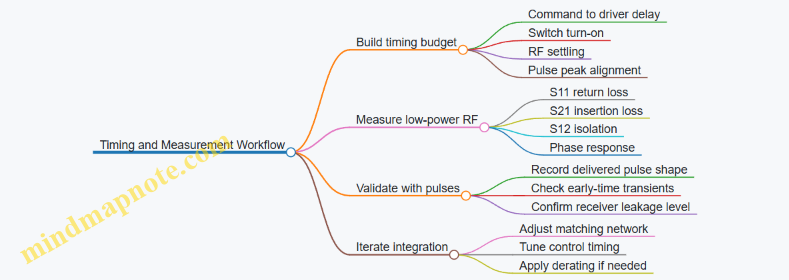
Fast routing is a system behavior, not just a component spec. When timing, impedance, isolation, and power handling are treated together, the switch becomes predictable—exactly what a pulse system needs.
4.5 Coaxial to Waveguide Transitions and High Power Connectors
High power microwave systems rarely stay in one geometry. A coaxial feed is convenient for instrumentation and compact packaging, while waveguide is often the practical choice for power handling and low loss at high frequencies. The job of a coaxial-to-waveguide transition is to move the electromagnetic field from a TEM-like coax mode into the dominant waveguide mode with minimal reflection, controlled phase, and safe power density.
Core Concepts and Design Targets
Start with the field picture. Coax supports a quasi-TEM mode whose transverse fields are set by the inner conductor and outer conductor geometry. Waveguides support discrete modes; for most power applications the dominant mode is the one with the lowest cutoff. A good transition ensures that the waveguide mode is excited efficiently and that the transition region does not create strong higher-order mode content.
Design targets are usually expressed as:
- Return loss and VSWR at the operating band, measured with the same connector and cable lengths used in the system.
- Power handling margin, based on peak surface electric field and temperature rise.
- Phase stability across the band, because system-level combining and beamforming can be sensitive to small phase shifts.
A practical best practice is to treat the transition as part of the RF chain, not as a standalone component. If the connector interface changes, the impedance environment changes too.
Mechanical Interfaces That Matter
High power connectors fail in boring ways: misalignment, poor contact pressure, and contamination. For coax-to-waveguide transitions, the mechanical stack includes the coax connector, the transition body, the waveguide flange, and the sealing surfaces.
Key practices:
- Use repeatable torque and a torque pattern, not “tight until it feels right.” Uneven clamping can distort the waveguide flange and shift the effective gap.
- Maintain concentricity between the coax center conductor and the transition center region. A small eccentricity can increase local field enhancement.
- Choose gasket and surface finish that survive thermal cycling. A gasket that relaxes after heating can create a new leakage path and a new reflection.
Transition Geometries and Mode Matching
Common approaches include:
- Probe or post transitions where a coax center conductor couples into the waveguide aperture region.
- Iris or slot transitions where the coax fields couple through a controlled discontinuity into the waveguide.
- Tapered transitions where the geometry gradually transforms the field distribution.
The systematic way to design is to pick a target waveguide mode, then shape the transition so the dominant field components overlap. For a probe-type transition, the probe length and diameter control coupling strength and the effective susceptance. For an iris-type transition, the iris thickness and aperture dimensions control how much electric field penetrates into the waveguide.
A simple example: if measured return loss is poor at the low end of the band, the transition is often under-coupled or the effective electrical length is too short. Increasing probe length or adjusting the iris aperture can shift the match, but it also changes the field concentration, so power handling must be re-checked.
High Power Connectors and Field Stress Control
Connectors are not just mechanical; they shape the local electromagnetic environment. At high power, the limiting factor is often the maximum surface electric field near:
- Center conductor terminations.
- Threaded interfaces and steps.
- Dielectric boundaries and any exposed sharp edges.
Best practices that are easy to apply:
- Avoid sharp corners on exposed conductors. A small radius can reduce field enhancement.
- Keep dielectric surfaces clean and dry. Even a thin contamination layer can raise loss and promote breakdown.
- Ensure the connector interface is designed for the same grounding scheme as the transition body. Floating or poorly bonded grounds create current crowding.
For waveguide flanges, the mating surfaces should be flat and consistent. A practical check is to verify that the RF contact surfaces are not visibly damaged after assembly and that the gasket does not intrude into the RF contact area.
Measurement and Verification Workflow
A transition can look perfect on paper and still misbehave in the lab because of assembly details. Use a verification workflow:
- Measure S-parameters with the transition assembled exactly as it will be used.
- Repeat measurements after disassembly and reassembly to quantify sensitivity to torque and alignment.
- Perform a power test with incremental steps while monitoring reflected power and temperature.
- Inspect post-test surfaces for discoloration, pitting, or residue.
If you see a return loss notch that shifts after reassembly, suspect mechanical tolerances or connector contact pressure rather than electromagnetic modeling error.
Mind Map: Coaxial to Waveguide Transitions
Example: Diagnosing a Mismatch After Assembly
Suppose a transition meets the target return loss in a bench setup, but the system measurement shows worse VSWR. A systematic approach is to isolate variables:
- Confirm that the coax connector is seated with the same torque and that the center conductor has the same protrusion.
- Check flange gasket placement and verify that the waveguide flange surfaces are clean.
- Compare S-parameters with and without the transition in the same fixture to ensure the fixture is not dominating the measurement.
If the mismatch is repeatable with assembly, the likely cause is mechanical tolerance sensitivity. If it varies randomly, suspect contamination, inconsistent contact pressure, or connector wear.
Example: Power Handling Improvement Without Changing Frequency
If power tests show early degradation, focus on field stress rather than only matching. Common fixes include:
- Smoothing or reworking sharp edges near the coupling region.
- Replacing worn connector parts that have micro-roughness or damaged plating.
- Cleaning and drying dielectric surfaces and confirming that no gasket material intrudes into RF contact areas.
After each change, re-measure return loss. A small geometric cleanup can improve both breakdown margin and match, but it can also shift the coupling slightly, so verification stays mandatory.
5. Transmission Line Design for High Power Operation
5.1 Impedance Control and Field Distribution in Transmission Lines
Impedance control is the practice of keeping the transmission line’s effective load seen by the source close to the intended value across the operating bandwidth and power level. When it works, the voltage and current waves travel with minimal reflection, and the field distribution inside the line stays predictable. When it doesn’t, reflections create standing waves, local field peaks, and extra heating—often in places you didn’t plan to stress.
Core Concepts That Tie Everything Together
A transmission line supports forward and reflected waves. The reflection coefficient at a discontinuity is
\[\Gamma = \frac{Z_L - Z_0}{Z_L + Z_0}\]
where \(Z_L\) is the load impedance and \(Z_0\) is the line characteristic impedance. The closer \(Z_L\) is to \(Z_0\), the smaller \(|\Gamma|\) becomes. In practice, “impedance control” means managing \(Z_0\) and the effective \(Z_L\) presented by transitions, connectors, and matching networks.
Field distribution follows from the same wave picture. For a lossless line, the instantaneous voltage and current are sums of forward and reflected components. That means the electric and magnetic fields are not uniform in the presence of reflections; they vary along the line with the standing-wave pattern.
Mind Map: Impedance Control and Field Distribution
From Geometry to Characteristic Impedance
Characteristic impedance \(Z_0\) is set by the line’s cross-sectional geometry and dielectric properties. For coaxial lines, \(Z_0\) depends primarily on the ratio of inner to outer conductor radii and the dielectric constant. For waveguides and planar lines, the relationship is different, but the principle is the same: small geometric changes shift \(Z_0\) and therefore change the reflection behavior.
A practical way to think about this is to treat fabrication as a controlled variation of geometry. If the dielectric constant is higher than expected, the guided wavelength shortens and the effective impedance changes. If the conductor spacing is off by a small amount, the fields redistribute, altering both \(Z_0\) and the local field intensity.
Discontinuities Create Local Mismatch and Field Peaks
Even if the line is designed for \(Z_0\), real hardware includes discontinuities: connector interfaces, flange steps, imperfect transitions, and abrupt changes in cross-section. Each discontinuity introduces an effective load impedance at that point, producing a reflection that travels back toward the source.
Field distribution is the “where” of the problem. With reflections, voltage maxima occur at positions where the forward and reflected waves add. Current maxima occur where voltage is minimized. The important engineering implication is that the electric field magnitude tends to be highest where voltage is highest, which can increase breakdown risk and surface heating.
Matching as Controlled Transformation
Matching networks and transitions aim to transform the load impedance into something closer to \(Z_0\) over the relevant bandwidth. A simple resistive match can reduce reflections at one frequency, but it often wastes power as heat and may not handle high power well.
Tapers and multi-section transformers distribute the impedance change gradually, reducing the effective reflection at each small step. The same idea applies to waveguide transitions: a smooth change in geometry reduces abrupt mode mismatch.
A useful rule of thumb for intuition: if the transition is electrically short compared to the wavelength, it behaves like a lumped discontinuity; if it is electrically longer, it can behave more like a distributed transformer. The design goal is to choose a length and shape that keep reflections small across the band.
Example: What VSWR Means for Field Distribution
Suppose a line is specified for \(Z_0 = 50,\Omega\) and the load is \(Z_L = 75,\Omega\). Then
\[\Gamma = \frac{75-50}{75+50} = \frac{25}{125} = 0.2\]
The voltage standing-wave ratio is
\[\text{VSWR} = \frac{1+|\Gamma|}{1-|\Gamma|} = \frac{1.2}{0.8} = 1.5\]
A VSWR of 1.5 means the voltage magnitude at maxima is 1.5 times the incident-wave voltage (and minima are 0.67 times). That ratio directly affects where the electric field is strongest along the line. If your system has a known weak point—like a connector edge or a surface roughness hotspot—this standing-wave pattern tells you whether the hotspot is likely to coincide with a voltage maximum.
Example: Tolerance and Alignment in a Transition
Consider a waveguide-to-coax transition where the intended geometry yields a good match. If machining tolerance shifts the effective aperture size, the transition’s effective impedance changes, increasing \(|\Gamma|\). The result is not just a worse S11; it also changes the standing-wave pattern, which can move voltage maxima closer to the transition region. That can increase local heating even if the average power is unchanged.
A good practice is to treat the transition as a system element with its own measurement signature. Measure S-parameters at the assembled interface, not just on individual parts. Then verify that the worst-case mismatch aligns with acceptable field limits for the specific hardware.
Verification Practices That Confirm the Field Story
S-parameters confirm mismatch, but field distribution is the physical consequence. Use VSWR and return loss to estimate reflection magnitude, then check time-domain behavior (for example, via reflectometry) to locate where reflections originate. If you see a reflection peak at a known connector or flange, you can focus on that discontinuity’s geometry, surface finish, and alignment.
Finally, remember that impedance control is not only about matching at one port. In multi-stage systems, each interface changes the effective load seen by the previous stage, so consistent impedance control across the chain prevents “fixing” one mismatch while creating another.
5.2 Skin Effect Proximity Effect and Surface Roughness Losses
High-power microwave lines fail in boring ways: fields concentrate where conductors are “least forgiving,” and losses rise faster than you expect. Three culprits dominate at RF and microwave frequencies: skin effect, proximity effect, and surface roughness. Together they determine the effective conductor resistance, which then sets ohmic loss, heating, and ultimately how much power you can push before temperatures and breakdown risk get cranky.
Core Idea of Skin Effect
At microwave frequencies, current crowds near the conductor surface because the time-varying magnetic field induces opposing fields inside the metal. The characteristic depth is the skin depth, δ, which shrinks as frequency rises. A practical rule: if your conductor thickness is much larger than δ, the current effectively flows in a thin shell, so the AC resistance per length grows roughly like 1/δ.
Easy example: take copper at 10 GHz. δ is on the order of a micrometer scale. A typical plated waveguide wall thickness is far larger, so the current is confined to the surface. If you double frequency, δ drops by about √2, and the conductor loss increases by about √2 for the same geometry and current distribution.
Proximity Effect from Nearby Conductors and Fields
Skin effect alone assumes each conductor carries current without strong influence from its neighbors. Proximity effect breaks that assumption: magnetic fields from currents in adjacent conductors alter the current distribution within each conductor. The result is non-uniform current density across the cross-section, often concentrating current on the sides facing other conductors or on the side facing the return path.
In waveguides and coaxial structures, proximity is common because the return current is not “far away.” In a coax, the inner conductor’s current distribution is influenced by the outer conductor’s current. In a rectangular waveguide, the field pattern and return paths make some walls carry more intense surface currents than others.
Easy example: consider two parallel conductors carrying equal and opposite currents. At low frequency, current spreads through the cross-section. At higher frequency, each conductor’s current is already near its surface (skin effect). Proximity then pushes it further toward the facing surfaces, increasing effective resistance compared with an isolated-conductor estimate.
Surface Roughness Losses
Even if you model the conductor as perfectly smooth, real surfaces have microscopic peaks and valleys. Roughness increases loss because it effectively increases the path length and enhances local current crowding. The impact depends on how roughness features compare to δ.
If the roughness height is small compared with δ, the current averages over the surface features and the loss increase is modest. If roughness features become comparable to or larger than δ, current follows the local geometry more closely, raising the effective resistance.
Easy example: imagine two copper surfaces with the same average roughness but different polishing directions. In one case, the peaks align with the dominant current flow direction and create more local crowding. The measured attenuation differs even though the bulk material is the same.
How These Effects Combine in Practice
The total conductor loss is not simply “skin loss plus roughness loss.” Proximity changes where current concentrates; roughness then changes how much extra resistance those concentrated regions experience. That means the worst-case heating often occurs at specific locations: facing walls in a tight geometry, corners where fields intensify, and plated interfaces where surface quality varies.
A systematic workflow for design checks:
- Estimate δ at the operating frequency to confirm the current confinement regime.
- Identify dominant current paths and return paths to anticipate proximity-driven redistribution.
- Use surface roughness parameters to adjust the effective surface resistance.
- Validate with temperature rise expectations under realistic duty cycle and cooling conditions.
Mind Map: Skin Effect Proximity Effect and Surface Roughness Losses
Example: Waveguide Wall Loss Hotspots
Suppose you have a rectangular waveguide operating in a mode where the magnetic field is strongest near two opposite walls. Those walls carry the highest surface current density. If the waveguide is built with a rougher finish on one wall (or a plating process that leaves higher micro-roughness), roughness loss becomes location-dependent. Proximity effect further increases current crowding on the walls where the return path geometry forces stronger magnetic coupling.
The engineering takeaway is simple: when you compute conductor loss, you need a model that respects both current confinement (skin effect) and current redistribution (proximity), then applies roughness where the current actually goes. That’s how you avoid the classic surprise where the average loss looks acceptable, but the hottest spot runs too hot.
5.3 Dielectric Selection and Thermal Stability for RF Materials
High-power RF systems punish dielectrics in two ways: they heat up, and their electrical properties drift as they heat up. Dielectric selection for thermal stability means choosing a material whose permittivity, loss tangent, and thermal expansion stay predictable under the actual temperature rise and field stress of the design.
Core Concepts for Thermal Stability
Start with the relationship between RF fields and heating. In a dielectric, RF power loss is commonly modeled as volumetric loss proportional to \(\omega\varepsilon’\varepsilon''\), where \(\varepsilon’\) sets stored energy and \(\varepsilon''\) (often expressed via loss tangent \(\tan\delta\)) sets dissipated energy. A practical consequence: if \(\tan\delta\) increases with temperature, the material becomes a self-heating loop—more heat causes more loss, which causes more heat.
Next, connect electrical drift to system behavior. Changes in \(\varepsilon’\) shift resonance frequencies in cavities and alter phase in transmission structures. Changes in \(\tan\delta\) change insertion loss and can reduce efficiency. Thermal stability is therefore not just “survive the temperature,” but “stay electrically consistent enough for the job.”
Material Properties That Matter in Practice
When comparing candidates, focus on properties that directly govern temperature rise and electrical drift.
-
Loss Tangent Versus Temperature Measure or obtain \(\tan\delta(T)\) at the operating frequency. A small increase can be acceptable if cooling keeps the steady-state temperature low. A large increase is a red flag even if the room-temperature loss looks fine.
-
Permittivity Versus Temperature Track \(\varepsilon’(T)\) or the temperature coefficient of permittivity. For resonant structures, frequency shift is roughly proportional to the change in effective permittivity. A dielectric with modest loss but strong permittivity drift can still cause detuning.
-
Thermal Conductivity and Heat Spreading Thermal conductivity \(k\) controls how quickly heat leaves the high-field region. Low \(k\) forces steep temperature gradients, which can create local hot spots and accelerate degradation.
-
Thermal Expansion and Mechanical Stress Mismatch in coefficient of thermal expansion between dielectric and metal surfaces can loosen interfaces or create microcracks. Those defects then raise loss and can initiate breakdown.
-
Moisture Sensitivity and Aging Many dielectrics absorb moisture or change microstructure with time. Moisture increases loss and can make \(\tan\delta\) vary unpredictably. Even if the initial performance is good, stability over repeated thermal cycles matters.
Mind Map: Dielectric Selection Workflow
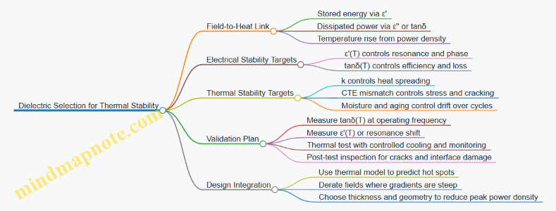
Systematic Selection Method with Examples
Step 1: Define the thermal and electrical acceptance limits. Example: Suppose a resonant waveguide section must stay within ±0.5% frequency shift during a pulse train. That requirement translates into a maximum allowable change in effective permittivity. If the dielectric’s \(\varepsilon’(T)\) implies that a 40 K rise causes 0.6% shift, then the design must keep the dielectric rise below about 35 K under steady operation.
Step 2: Estimate temperature rise from RF loss. Use a thermal model that includes conduction paths and realistic boundary conditions. A quick sanity check: if the dielectric volume experiences high electric field while cooling is limited, the peak temperature can exceed the average by several times. That’s why “average power” alone is not enough.
Step 3: Screen materials using temperature-dependent loss. Example: Two candidates have the same room-temperature \(\tan\delta\). Material A’s \(\tan\delta\) doubles by 80 °C; Material B’s increases by 20%. If your predicted steady-state dielectric temperature is 70 °C, Material A will likely produce much higher insertion loss and may push the system into a thermal runaway region.
Step 4: Check permittivity drift against the system’s tuning margin. Example: In a cavity, a dielectric with strong \(\varepsilon’(T)\) may detune the resonance during a pulse burst. If the system has a tuner, you can compensate for slow drift, but fast pulse-to-pulse drift still affects phase and matching.
Step 5: Verify mechanical integrity under thermal cycling. Example: A dielectric bonded to metal with a large CTE mismatch can develop interfacial gaps after repeated heating. Those gaps increase local fields and loss. A practical mitigation is to choose a dielectric whose CTE is closer to the metal and to design the bondline thickness so it can tolerate expansion without cracking.
Practical Example: Choosing Between Two Dielectrics
Imagine selecting a dielectric for a high-power matching insert. Candidate X has higher thermal conductivity but higher loss at elevated temperature. Candidate Y has lower room-temperature loss but poor heat spreading.
A good decision comes from comparing predicted steady-state temperatures and resulting loss. If Candidate X keeps the dielectric 25 K cooler and its \(\tan\delta\) rise is moderate, it can outperform Candidate Y even when X starts with a slightly worse room-temperature loss. The “better” material is the one that minimizes \(\text{loss} \rightarrow \text{heating} \rightarrow \text{more loss}\) under your actual cooling and geometry.
Validation Checklist for Thermal Stability
- Measure \(\tan\delta(T)\) at the operating frequency range.
- Confirm \(\varepsilon’(T)\) or resonance shift behavior in a representative structure.
- Use a thermal model that includes heat spreading and realistic boundary conditions.
- Run a thermal test with monitoring that can detect hot spots, not just average temperature.
- Inspect after cycling for cracks, delamination, and interface degradation.
When these steps agree—electrical stability, thermal stability, and mechanical integrity—you get a dielectric choice that behaves predictably under high-power stress. That predictability is the real win, not just a low loss number on a datasheet.
5.4 Matching Networks Including Tuners and Broadband Matching
High power microwave systems rarely behave like the textbook “perfect 50 Ω load.” Matching networks exist to reduce reflections, protect sources from high VSWR, and keep field distributions predictable inside waveguides and resonators. The key idea is simple: you shape the impedance seen by the source so that the wave leaving the source mostly continues forward instead of bouncing back.
Core Concepts for Matching
Start with the reflection coefficient at the input plane, \(\Gamma = (Z_L - Z_0)/(Z_L + Z_0)\). When \(\Gamma \to 0\), the load absorbs power with minimal return loss. In practice, you match not only the magnitude of impedance but also the phase relationship across frequency.
A useful mental model is to treat the network as an impedance transformer plus a frequency-shaping filter. A narrowband tuner can make \(\Gamma\) small at one frequency, while a broadband network aims to keep \(\Gamma\) small over a range.
Smith Chart Workflow with Practical Constraints
A systematic workflow looks like this:
- Identify the reference plane where you want matching to occur (often at the waveguide interface or at the amplifier output).
- Measure or estimate the complex load impedance versus frequency using low-power S-parameters.
- Convert to normalized impedance \(z = Z/Z_0\) and plot on a Smith chart.
- Choose a network topology that can move the point toward the center (\(\Gamma=0\)) using realizable elements.
- Check high power limits: peak surface fields, breakdown risk, and thermal drift.
A tuner that “works” on a Smith chart can still fail in hardware if the required adjustment creates sharp field concentrations or overheats a dielectric.
Tuners for High Power Waveguide Systems
Waveguide tuners commonly use mechanical motion to change the effective electrical length or susceptance.
- Slotted line and probe-based tuning: A probe changes coupling to a resonant or reactive load. It’s precise but can be sensitive to alignment.
- E-plane or H-plane tuning screws: A screw changes boundary conditions and therefore the input reactance.
- Staged tuners: Two degrees of freedom (e.g., one for reactance, one for conductance) reduce the chance that you can only match at one frequency.
Easy example: Suppose your load looks inductive at the operating frequency. A single tuning screw can cancel the reactive part, but the residual mismatch may remain because the conductance is not right. Adding a second element that adjusts the coupling strength can reduce reflections without demanding extreme screw positions.
Broadband Matching Strategies
Broadband matching is harder because you must control impedance behavior across frequency, not just at one point. Three practical strategies dominate.
-
Use inherently broadband transformations
- Tapered transitions (e.g., waveguide-to-waveguide or coax-to-waveguide) spread the transformation over length, reducing abrupt impedance steps.
- Multi-section transformers approximate a smooth impedance ramp.
-
Employ multi-element matching networks
- Two- or three-element L/C or waveguide-section equivalents can be designed for a target return loss over a band.
- The trade is size and sensitivity: more sections usually improve bandwidth but increase fabrication tolerance demands.
-
Accept controlled mismatch with system-level tolerance
- If the source can tolerate some VSWR and the load is robust, you may design for “good enough” reflection across the band.
- This is not a cop-out; it’s a deliberate allocation of performance where it matters most.
Easy example: If your system operates from 9.0 to 9.5 GHz, a single resonant matching element might give excellent match at 9.2 GHz but poor match at the edges. A two-section transformer can keep the input reflection coefficient low at both ends by distributing the impedance change.
High Power Design Checks for Tuners and Match Networks
Matching networks must survive the electrical environment they create.
- Field concentration: Sharp corners, small gaps, and over-tight screw positions can raise local electric fields and trigger breakdown.
- Thermal drift: Mechanical tuners can shift under heating; even small dimensional changes can move the match point.
- Surface roughness and loss: At high power, conductor losses and heating can change the effective impedance, especially in narrow gaps.
- Mechanical stability: Locking mechanisms should prevent creep and vibration-induced mismatch.
A practical best practice is to tune at the lowest power first, then re-check at representative power levels while monitoring temperature and return loss.
Mind Map: Matching Networks Including Tuners and Broadband Matching
Worked Example: Choosing Between a Tuner and a Broadband Network
If your load impedance varies strongly with frequency but your operating bandwidth is narrow, a tuner is efficient: you can cancel the dominant reactive mismatch at the center frequency and accept small edge degradation. If your bandwidth is wide and the load is stable, a broadband transformer or multi-section network reduces the need for repeated adjustments and lowers sensitivity to small mechanical changes.
In both cases, the matching design should be evaluated with the same mindset: the network is not just an equation on paper; it is a physical structure that must handle the fields and temperatures it creates.
5.5 S Parameter Measurement Techniques Under High Power Conditions
High power S-parameter measurements are less about “getting numbers” and more about preventing the measurement setup from becoming the limiting component. At low power, a VNA assumes the DUT is linear and the test ports behave ideally. At high power, the DUT may compress, heat, or arc, and the measurement chain can introduce its own nonlinearities. The goal is to measure what the DUT does to forward and reflected waves while keeping the test system stable and protected.
Core Concepts for High Power S Parameters
Start with the definition: S11 and S21 describe how incident waves at the reference planes are reflected and transmitted. Under high power, the reference planes still matter, but the calibration must also account for power-dependent behavior in adapters, cables, and couplers. A practical approach is to measure at multiple power levels and treat each level as its own operating point.
Two practical constraints dominate:
- Linearity window: If the DUT is nonlinear, S-parameters become power-dependent and may not represent a single small-signal transfer function.
- Thermal and breakdown margins: Even if the DUT is “fine” electrically, local heating can change impedance, and small gaps can arc.
A simple sanity check is to compare repeated sweeps at the same power. If the trace drifts, you are measuring drift, not just RF behavior.
Measurement Setup and Reference Plane Discipline
Use a high-power-capable test path with components rated for the peak and average power, including connectors and transitions. Place the VNA reference planes at the DUT interfaces as much as the hardware allows. If you cannot physically move the reference planes, you must characterize the additional path and keep it consistent.
A typical chain includes:
- VNA with appropriate source power control
- High power directional coupler or power sensor path
- Waveguide or coax switchable test fixtures
- DUT under test
- Isolation and protection elements
Protection is not optional. Add fast shutdown or interlocks triggered by reflected power thresholds, temperature sensors, or arc detection signals from the fixture.
Calibration Strategies That Survive Power
At high power, calibration is not just “do SOLT once.” You need a calibration that remains valid across the power range.
- Perform a standard calibration at low power to establish baseline port behavior.
- Verify power dependence by measuring a known-through or known-match structure at increasing power.
- Use a power-aware approach: if your coupler has directivity or coupling that varies with power, correct it using characterization data or by selecting a coupler designed for stable coupling.
If you use waveguide fixtures, ensure the mechanical repeatability is tight. Re-mounting the DUT can change contact pressure and surface conditions, which changes reflection.
Time Domain and Pulse-Aware Measurements
Many high power microwave systems are pulsed. In that case, you should measure S-parameters in a way that respects the pulse envelope.
- For pulsed operation, use a VNA mode or external gating that captures the steady portion of the pulse.
- Keep the pulse width long enough for the DUT to reach its quasi-steady thermal state if you want thermal effects, or short enough to isolate purely electrical behavior.
A practical example: measure S11 at the start of the pulse and near the end. If S11 moves significantly, the DUT impedance is evolving during the pulse.
Advanced Details for Reliable Data
Directional coupler behavior: Couplers can saturate or change directivity at high power. If directivity collapses, the reflected wave estimate becomes noisy or biased.
Connector and transition effects: A small mismatch at a transition can create a hot spot. Treat transitions as part of the measurement chain and keep them identical across runs.
Thermal stabilization: If the DUT is thermally sensitive, allow a consistent warm-up procedure. Then measure at fixed intervals so each sweep corresponds to a known thermal state.
Trace consistency checks: Run a short “repeat sweep” at the same power. If the magnitude changes more than your expected measurement uncertainty, stop and identify the cause.
Mind Map: High Power S Parameter Measurement Workflow
Example: Measuring S11 Compression in a Waveguide DUT
Assume a waveguide DUT that is expected to compress at higher drive. Use a waveguide test fixture with a rated directional coupler. Calibrate at low power, then measure S11 at three power levels. Keep the pulse width fixed and use the same warm-up time before each sweep.
What to look for:
- Magnitude trend: If |S11| decreases with power, the DUT is changing its input impedance under drive.
- Frequency-dependent reshaping: A shift in the frequency where |S11| is minimal suggests the resonant behavior is moving due to heating or nonlinear reactance.
- Repeatability: If the S11 curve differs between identical sweeps, the DUT or fixture is not in a stable state.
If you see sudden spikes in the reflected estimate at a specific power, check coupler saturation and verify that the reflected-power protection threshold is not triggering intermittently.
Example: Pulse Gating to Separate Electrical and Thermal Effects
For a pulsed DUT, measure S21 using a gated acquisition that targets the early part of the pulse. Repeat the measurement targeting the late part. If early S21 matches the low-power trend while late S21 shows reduced transmission, the dominant mechanism is thermal impedance change rather than immediate nonlinear mixing.
This two-window method is especially useful when the DUT is close to a mismatch threshold where small heating changes can noticeably alter reflections.
6. Pulse Modulators and High Voltage Drive Systems
6.1 Pulse Requirements Including Rise Time Width and Repetition Rate
High power microwave systems are usually constrained by three pulse parameters: rise time, pulse width, and repetition rate. Together they determine peak fields, average heating, electron beam loading, and the time budget for protection circuits. A good practice is to start from the electromagnetic requirement (what field and energy you need at the load) and then work backward to the pulse generator and switching chain.
Pulse Rise Time
Rise time is the time for the RF envelope to move from a low level to a specified fraction of its final value. In practice you care about the 10–90% definition because it correlates well with bandwidth stress in the modulator, transmission path, and device input.
A fast rise time increases spectral content. That means more energy in frequency components that may not be well matched, which can raise reflections and stress components not designed for those transient conditions. For an easy example, consider a 1 µs pulse with a 10 ns rise time versus a 100 ns rise time. The faster edge spreads energy across a wider band, so even if the steady-state match is good, the initial transient can see higher VSWR and produce larger peak currents in couplers and switches.
Best practice: specify rise time at the load plane, not just at the modulator output. Use a directional coupler and a fast detector or sampling scope to confirm the actual envelope shape after the full RF chain.
Pulse Width
Pulse width sets the duration of sustained power at the load. For many thermal and reliability concerns, pulse width matters more than you might expect because heating depends on energy deposited over time, not only on peak power.
A useful rule of thumb is to separate effects:
- Electromagnetic stress and breakdown risk often correlate with peak electric field, which is tied to rise time and peak power.
- Thermal rise correlates with average power over the pulse train, which depends on pulse width and repetition rate.
Example: If you keep peak power constant and double pulse width while halving repetition rate, the average power can remain similar, but the device may still experience different internal temperature gradients. Longer pulses give more time for heat to soak into interfaces, which can shift breakdown behavior from surface-limited to bulk-limited mechanisms.
Best practice: define pulse width tolerance. A 5% width error can be harmless in a purely electromagnetic experiment, but it can be significant when your protection thresholds or thermal models assume a specific duty cycle.
Repetition Rate
Repetition rate determines duty cycle and therefore average heating and cumulative fatigue. Duty cycle is simply the fraction of time the system is delivering RF power:
- Duty cycle = pulse width × repetition rate.
If your pulse width is 2 µs and repetition rate is 1 kHz, the duty cycle is 0.2%. That number is small, but it still drives average temperature rise and can change gas breakdown margins in waveguides or switch gaps.
Repetition rate also interacts with recovery times:
- Switching devices need time to deionize or cool.
- Resonant structures need time to settle if you are using pulsed excitation.
- Control loops need time to correct bias or compensate droop.
Best practice: treat repetition rate as a system-level constraint. Even if the RF chain can handle the duty cycle, the modulator and protection hardware may be the limiting factors.
Integrated Design Logic
A systematic workflow is to compute required peak and average quantities, then map them to pulse parameters and hardware limits.
- Start with required energy and peak field at the load.
- Choose rise time based on allowable transient stress and available modulator bandwidth.
- Choose pulse width to meet energy delivery while staying within thermal limits.
- Choose repetition rate to satisfy average heating and recovery constraints.
- Verify with measurements of envelope shape, not just average power.
Mind Map: Pulse Requirements
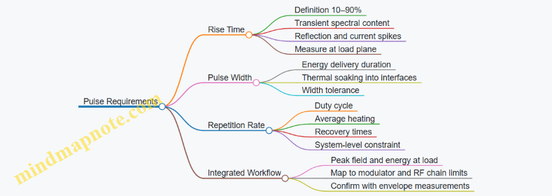
Example: Parameter Selection with Constraints
Suppose you need 50 kW peak at the load for a 2 µs pulse train. You also know the modulator chain can produce a 20 ns rise time at the output, but the RF path includes a waveguide section with a known mismatch risk during transients.
- If you accept 20 ns rise time at the modulator output, you must verify the rise time at the load because the transient may reflect and distort the envelope.
- If the measured load rise time is slower, peak field may reduce slightly, which can affect breakdown margin.
- For thermal safety, you compute duty cycle from pulse width and repetition rate. If the allowable average power corresponds to a duty cycle of 0.5%, then with 2 µs pulses the maximum repetition rate is 2500 Hz.
The key point is that rise time, width, and repetition rate are not independent knobs. Changing one parameter changes both the transient stress profile and the cumulative thermal state.
6.2 Marx Generators and Capacitor Bank Pulse Formation
A Marx generator creates a high-voltage pulse by charging many capacitors in parallel to a moderate voltage, then switching them into series for a short time. The key idea is simple: series connection multiplies voltage, while the pulse width is set mainly by the switching network and the load’s effective impedance.
Core Principle and Energy Accounting
During the charge phase, each capacitor charges to approximately \(V_0\). If \(N\) capacitors are switched into series, the ideal output voltage is about \(N V_0\). In practice, the output is reduced by switch voltage drops, stray inductances, and capacitor voltage imbalance.
A useful sanity check is energy. The stored energy per capacitor is \(\tfrac{1}{2} C V_0^2\). Total stored energy is \(\tfrac{1}{2} N C V_0^2\) (for identical capacitors). Not all of this becomes load energy: some is dissipated in switches, resistive losses, and in the load’s mismatch. This is why “more voltage” alone does not guarantee “more delivered pulse.”
Charging Phase Best Practices
- Use a controlled charging supply with current limiting. Capacitor charging is not a gentle activity; current spikes can stress components and create uneven charging.
- Balance capacitor voltages. Even small capacitance tolerances or leakage differences can cause one stage to reach breakdown earlier.
- Include bleed resistors. They discharge capacitors when the system is off, reducing residual charge hazards and improving repeatability.
Example: If you need 60 kV peak with 10 stages, the ideal stage charge is 6 kV. If one stage leaks more, its voltage may sag by 5%, reducing the output by roughly 5% of one stage’s contribution.
Switching Phase and Pulse Formation
The pulse begins when the switches (often spark gaps or thyratrons) trigger sequentially. In an ideal Marx, all stages transition quickly enough that the output resembles a flat-topped pulse. Real systems show a ramp or droop due to:
- Stray inductance in the loop paths, which limits current rise.
- Switch jitter, which spreads the effective series connection over time.
- Load interaction, where the load draws current and discharges the equivalent capacitance.
A practical way to estimate pulse droop is to treat the series-connected capacitors as an equivalent capacitance \(C_{eq} \approx C/N\) (for identical capacitors). The load current discharges the capacitor network, so the voltage falls roughly according to \(\Delta V \approx I \Delta t / C_{eq}\). This is why pulse width and load current cannot be chosen independently.
Equivalent Circuit View That Engineers Actually Use
During the pulse, the Marx can be modeled as a high-voltage source with an internal capacitance and series inductance feeding the load. The load sees a voltage that depends on the current drawn and the mismatch between the load and the effective source impedance.
Rule of thumb: if the load is much higher impedance than the source, the pulse voltage stays closer to the ideal value but current is small; if the load is low impedance, voltage droops faster.
Mind Map: Marx Generators and Capacitor Bank Pulse Formation
Integrated Example with Numbers
Assume 10 stages, each capacitor \(C = 5,\mu\text{F}\), charged to \(V_0 = 6,\text{kV}\). The ideal peak is \(N V_0 = 60,\text{kV}\). The equivalent capacitance is \(C_{eq} \approx C/N = 0.5,\mu\text{F}\).
If the load draws an average current of \(I = 20,\text{A}\) for \(\Delta t = 2,\mu\text{s}\), the approximate droop is: \[ \Delta V \approx \frac{I\Delta t}{C_{eq}} = \frac{20\times 2\times 10^{-6}}{0.5\times 10^{-6}} \approx 80,\text{kV} \] That result is clearly not physical because the voltage cannot drop below zero; it tells you the assumed current and pulse width are incompatible with the available capacitance. In practice, you would reduce current (higher load impedance), shorten pulse width, increase capacitance, or increase the number of stages/capacitor size while keeping switch limits in view.
Practical Implementation Notes
- Stage layout matters. Minimize loop area to reduce inductance and ringing.
- Trigger distribution should be symmetric. Unequal cable lengths and trigger delays create stage timing errors.
- Use instrumentation that matches the waveform. A probe with the wrong bandwidth can make a drooping pulse look like a flat one, or vice versa.
A Marx generator is therefore less about “stacking voltage” and more about managing timing, impedance, and energy flow so the load sees the intended pulse shape without overstressing the switching network.
6.3 Thyratron and Solid State Switching for Pulse Delivery
High power microwave pulse delivery needs two things at once: fast, repeatable switching and predictable behavior under high RF and high voltage stress. The switch sits between the modulator and the RF chain, so its job is not only to turn power on and off, but also to preserve pulse shape, limit reflections, and survive the electrical and thermal punishment.
Core Switching Requirements
A practical pulse switch is judged by rise time, jitter, on-state voltage drop, off-state isolation, and recovery behavior after turn-off. For example, if a radar transmitter requires a 1 µs pulse with a 10 ns rise time, the switching element must settle quickly enough that the RF envelope reaches the intended level before the system starts timing measurements. If the switch turns off slowly, the falling edge smears and can corrupt range resolution.
Pulse delivery also has a “system reality” constraint: the switch must match the impedance environment it sees. A thyratron or solid state device driving a transmission line will create reflections if its effective impedance changes during switching. Those reflections can re-trigger breakdown in weak spots or distort the pulse amplitude.
Thyratron Switching Fundamentals
A thyratron is a gas-filled switching tube that conducts when the electric field triggers breakdown and the device transitions into a stable conducting plasma state. Key behaviors include:
- Triggering: A control grid pulse initiates conduction, but the exact delay depends on gas conditions, electrode geometry, and drive amplitude.
- Conduction: Once conducting, the tube behaves like a low-impedance path with a voltage drop that depends on current and plasma state.
- Turn-off: The tube stops conducting when current falls below a holding level and the plasma cools and deionizes.
A simple way to picture it: the thyratron is like a gate that opens reliably when you push the right button, but it closes only after the “current tide” recedes enough for the water to calm.
Solid State Switching Fundamentals
Solid state switching uses semiconductor devices such as MOSFETs, IGBTs, or fast diodes in configurations that handle high voltage and current. The main advantages are tight control of timing and lower maintenance. The main challenges are voltage stress, switching losses, and the need for series/parallel device stacks to reach high pulse voltages and currents.
Solid state switches tend to have more deterministic turn-on and turn-off, but they can be sensitive to overvoltage spikes caused by stray inductance in the pulse path. Those spikes can exceed device ratings even when average voltages look safe.
Mind Map: Switching Tradeoffs
Integrated Design Practices for Pulse Delivery
1. Match the pulse path, not just the switch. Treat the modulator output, switch, and transmission line as one impedance system. If the switch introduces a different effective impedance during turn-on, the pulse will ring. A practical practice is to measure the pulse at the load with a fast probe and compare it to a baseline with a known-good termination.
2. Control stray inductance. Both thyratrons and solid state stacks suffer when wiring inductance creates voltage overshoot. Keep loop areas small, use compact layouts, and place current return paths close to the forward path. A quick sanity check is to estimate the inductive voltage spike as V = L·di/dt; if the spike approaches device limits, the layout is the problem, not the schematic.
3. Use protection that respects pulse energy. Overcurrent and overvoltage protection must be designed for the pulse regime. For example, a protection element that is fine for steady-state operation may overheat during a repetitive pulse train. Place fast sensing close to the switch and ensure the protection action time is shorter than the time it takes for damage to accumulate.
Example: Choosing Between Thyratron and Solid State
Suppose a system needs 50 kV pulses with 200 A peak current and 1 µs pulse width at 100 Hz. A thyratron often fits because it naturally handles large peak currents and high voltage pulses with a single device path. If the same system also requires very consistent timing to within a few nanoseconds across temperature and repetition rate, solid state may be preferred, but only if the design can manage voltage spikes and provide adequate thermal headroom.
In practice, many designs start from the pulse requirements and then check the “hidden constraints”: allowable jitter, acceptable pulse droop, and the maximum safe switching stress including inductive overshoot.
Example: Pulse Shape Preservation Through Damping
Consider a modulator that produces a flat-top pulse but the measured output shows oscillations at the rising edge. That pattern often indicates an impedance mismatch or insufficient damping between the switch and the load. Adding or adjusting series resistance, using proper termination at the load, and ensuring the switch sees the intended load impedance during the transition can reduce ringing. The key is to verify the fix by measuring both the switch-side and load-side waveforms so you know where the mismatch lives.
Operational Considerations and Verification
For thyratrons, verify trigger delay distribution and recovery behavior by measuring timing over many pulses at representative repetition rates. For solid state, verify safe operating area under the actual pulse train, including heating effects from switching losses and conduction. In both cases, confirm that the RF chain sees a stable envelope: switching artifacts that look small at the modulator can become large after amplification or in sensitive RF components.
Mind Map: Verification Checklist
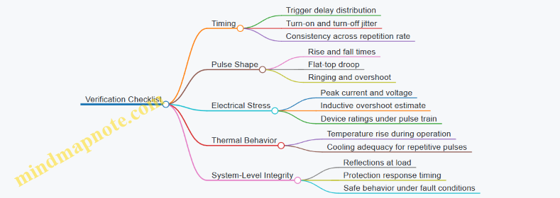
Summary
Thyratrons provide high peak power switching with plasma-based conduction and current-dependent turn-off, while solid state switches provide more deterministic timing but require careful control of voltage stress, inductance, and thermal limits. Good pulse delivery comes from treating the switch and pulse path as one system, then verifying timing and pulse shape at the load where the RF chain actually cares.
6.4 Pulse Transformers and Impedance Matching for Modulators
Pulse modulators often need two things at once: (1) a high-voltage pulse with a controlled shape, and (2) an RF-friendly impedance environment so the switching device and the load don’t fight each other. A pulse transformer helps with voltage step-up or step-down, isolation, and pulse shaping through its leakage inductance and parasitic capacitances. Impedance matching then turns those non-idealities from “surprises” into predictable behavior.
Core Concepts for Pulse Transformer Behavior
A pulse transformer is not a sinusoidal transformer. During a fast edge, the primary sees a time-varying impedance dominated by magnetizing inductance at low frequencies and by leakage inductance plus inter-winding capacitance at higher frequencies. The key practical quantities are:
- Turns ratio: sets the ideal voltage scaling, but only if the magnetizing current stays reasonable.
- Leakage inductance: limits current transfer and creates overshoot or ringing when combined with stray capacitances.
- Magnetizing inductance: draws current even with no load; too small a value increases primary current and distorts the pulse.
- Inter-winding capacitance: forms a high-frequency path that can couple the primary switching edge into the secondary.
A simple mental model is a transformer ideal ratio in series with leakage inductance, with a shunt capacitance across the windings. That model explains why a “perfect” turns ratio still yields a less-than-perfect pulse.
Impedance Matching Goals in Modulator Systems
Matching is about controlling reflections and energy storage. The modulator output stage typically drives a load that includes the device input impedance (often nonlinear) plus the pulse-forming network and transmission path. If the effective impedance seen by the switching device differs from its intended load, you get:
- Voltage overshoot that can exceed insulation margins.
- Current spikes that stress switches and transformer windings.
- Pulse droop from energy being trapped in reactive elements.
A practical goal is to make the transformer-secondary plus load look like a resistive target over the pulse bandwidth. Because the bandwidth is set by rise time, matching must be designed for the edge, not just the pulse width.
Mind Map: Pulse Transformer and Matching Workflow
Equivalent Circuit and How It Guides Design
Start with an equivalent circuit that includes: ideal transformer ratio, primary and secondary leakage inductances, magnetizing inductance, and shunt capacitances. Then add the modulator switching source impedance and the load termination. The matching strategy is usually implemented in two layers:
- Transformer-level matching: choose turns ratio and winding geometry so the secondary sees the right effective impedance during the edge.
- System-level matching: add series or parallel resistive elements (often with damping) so the combined network behaves well across the relevant bandwidth.
A useful rule of thumb: if ringing frequency is too high, it often comes from too much leakage inductance or too little damping. If the pulse droops early, magnetizing current or insufficient energy transfer is often the culprit.
Example: Matching a 50 Ω Pulse Source to a High-Voltage Load
Assume a modulator output stage behaves like a source with a 50 Ω Thevenin impedance and must deliver a pulse to a load that is effectively 200 Ω at the relevant timescale. A direct connection would cause reflections because the load is not equal to the source impedance.
A pulse transformer can step the impedance. The ideal impedance transformation is:
- Z_secondary ≈ Z_primary × (N_secondary / N_primary)^2
If the goal is to make the load look like 50 Ω to the source, you want the secondary-side effective impedance to be 50 Ω. With a 200 Ω load, choose the ratio so that:
- 50 ≈ 200 × \( N_secondary / N_primary \)^2
- \( N_secondary / N_primary \)^2 ≈ 0.25
- N_secondary / N_primary ≈ 0.5
So the secondary turns are about half the primary turns. In practice, you also include leakage inductance and add a damping resistor so the edge doesn’t excite a high-Q resonance. The damping resistor is selected to critically damp the dominant LC formed by leakage inductance and effective capacitance.
Example: Using Leakage Inductance for Pulse Shaping Without Surprises
Suppose measurements show that the transformer leakage inductance plus stray capacitance creates a ringing component with a period comparable to the pulse rise time. If you simply “tune” the turns ratio, the ringing persists because it’s set by L and C, not by the ideal ratio.
A systematic fix is to add a termination or snubber that increases effective damping. For instance, placing a resistor across the secondary (or in series with the load path, depending on topology) reduces the Q of the ringing mode. You then verify with a time-domain simulation using the measured parasitics, because the switching edge couples through capacitances and changes the effective damping during the first few nanoseconds.
Practical Implementation Checks
- Measure parasitics: extract leakage inductance and inter-winding capacitance from impedance sweeps or step-response tests.
- Terminate the right place: ensure the transmission path is terminated so reflections don’t re-enter the transformer.
- Control layout inductance: keep loop areas small; stray inductance can defeat matching even when the schematic looks correct.
- Validate with the real edge: matching designed for a slower rise time can fail when the switch delivers a faster edge.
Case Study: Matching That Fails and How to Fix It
A modulator transformer is built to deliver a clean pulse, but the observed waveform shows early overshoot and then a slow droop. The overshoot indicates underdamping of the leakage-inductance and capacitance resonance. The droop suggests either excessive magnetizing current (magnetizing inductance too low or core not biased as expected) or insufficient energy transfer due to a mismatch that causes reflections to return during the pulse.
The fix is two-step: first, add or adjust a damping/termination network to suppress the dominant ringing mode. Second, re-check magnetizing inductance and source impedance interaction, then update the equivalent circuit and re-run time-domain simulation. After that, the pulse shape becomes repeatable because the system is matched for the edge behavior, not just the steady pulse level.
6.5 Protection and Interlocks for High Voltage and RF Coexistence
High power microwave systems often combine two “unfriendly neighbors”: high voltage (HV) that can arc, and RF that can trigger breakdown, heat surfaces, and stress insulation. Protection and interlocks exist to prevent the system from ever reaching a hazardous combination of states. The core idea is simple: define safe operating conditions, detect violations early, and force the system into a known safe state faster than damage can accumulate.
Defining Hazard Pairs and Safe States
Start by listing the hazardous pairings you must avoid. Common ones include HV present while the RF path is open, HV enabled while a vacuum or cooling condition is missing, and RF enabled while a door, cover, or waveguide cover is not secured. For each pairing, define a safe state that is both electrically and mechanically benign.
A practical safe-state pattern is:
- RF drive disabled (or reduced to a harmless level)
- HV pulse inhibited (or HV ramp blocked)
- Energy discharge confirmed (where applicable)
- Interlock status latched and reported
Example: If a waveguide section is removed for inspection, the system should not merely “warn.” It should block HV pulse generation and RF enable simultaneously, because either one can create a path for arcing or unexpected coupling.
Interlock Types and What They Must Guarantee
Interlocks come in layers, because no single sensor is perfect.
- Hard interlocks: Must prevent enabling HV or RF. They are typically implemented with series logic and require deliberate reset.
- Soft interlocks: Provide controlled shutdown or inhibit with less stringent timing, often based on monitoring trends.
- Protection trips: Fast actions triggered by fault thresholds such as overcurrent, arc detection, or reflected power spikes.
Each interlock should specify what it guarantees: “HV cannot be pulsed,” “RF cannot exceed X,” or “energy is discharged below Y.” If you cannot state the guarantee in one sentence, the interlock is probably too vague.
Timing and Race Conditions
Protection logic must consider timing. A common failure mode is a race: RF is enabled a few milliseconds before HV, or HV is released while a discharge circuit is still draining.
Use a state machine mindset:
- Preconditions: vacuum, cooling flow, doors closed, grounding verified
- Arming: logic checks pass; system waits for discharge timers
- Enable: RF and HV are allowed only in the correct order
- Run: protection monitors are active
- Fault: immediate inhibit and controlled discharge
Example: If your modulator uses a capacitor bank, add a discharge timer interlock so that HV pulse enable is blocked until the bank voltage is below a defined threshold.
Sensor Selection and Signal Conditioning
Interlocks are only as good as their signals.
- Door and cover switches: Use redundant contacts for critical enclosures.
- Vacuum and pressure: Prefer sensors with clear thresholds and stable behavior across temperature.
- Cooling: Monitor flow rate and temperature rise, not just “pump running.”
- RF path integrity: Use directional couplers or return-loss monitoring to detect unexpected reflections that can precede breakdown.
- Arc detection: Combine fast electrical indicators (current spikes) with RF indicators (sudden broadband bursts) when possible.
Condition signals with filtering and hysteresis so that normal transients don’t cause nuisance trips. But keep the protection thresholds fast enough to stop damage.
Fault Handling and Energy Management
When a fault occurs, the system should move to a safe state deterministically.
A good fault response includes:
- Immediate inhibit of HV pulse command
- Immediate RF drive disable or power reduction
- Latching of the fault reason
- Controlled discharge of stored energy
- Verification that discharge completed before allowing reset
Example: If reflected power exceeds a set limit during a pulse, inhibit the next pulse and require a manual reset after the discharge timer completes. This prevents repeated “try again” behavior that can erode surfaces.
Mind Map of Protection Logic
Mind Map: Protection and Interlocks for HV and RF Coexistence
Integrated Example Workflow
Consider a pulsed system with a modulator, a waveguide output, and a circulator.
- Before arming: door closed, grounding verified, cooling flow present, vacuum above threshold.
- Discharge verification: capacitor bank voltage confirmed below the safe threshold.
- Arming: system allows RF enable only after HV inhibit is active; this prevents accidental RF-only operation from coupling into an unprepared HV stage.
- Enable sequence: HV pulse command and RF drive are enabled in the defined order with a short, fixed delay.
- During run: reflected power and arc indicators are monitored continuously.
- Fault: if reflected power exceeds limit or an arc indicator triggers, inhibit HV pulses immediately, disable RF drive, latch the fault, and require reset after discharge completion.
This workflow keeps the system from “almost safe” states, which is where most real-world damage tends to start: not from a dramatic failure, but from repeated small violations that the hardware can’t tolerate.
7. Thermal Management and Mechanical Design for Power Handling
7.1 Heat Transfer Models for RF Structures and Interfaces
High power RF hardware fails in the boring ways: temperatures rise, materials soften, interfaces degrade, and breakdown becomes easier. Heat transfer models are the tool that turns “it got hot” into numbers you can design around. The goal is not perfect prediction; it is reliable ranking of designs and identification of the dominant thermal bottleneck.
Core Physical Picture
Start with energy conservation: the RF source deposits power into the structure, and that power must leave through conduction, convection, and radiation. In waveguides and resonators, the dominant path is usually conduction through metals and dielectrics, then convection to a coolant or air. Radiation matters mainly at surfaces with poor convection or at elevated temperatures.
A practical modeling workflow uses two layers:
- Electromagnetic loss distribution gives where heat is generated (e.g., surface current loss on waveguide walls).
- Thermal network or field model transports that heat to sinks (coolant channels, mounting surfaces, heat spreaders).
Interface Modeling Starts with Thermal Resistance
Interfaces are where good designs go to die—mostly because contact resistance is real. Model an interface as a thermal resistance element:
- Conduction through bulk: depends on geometry and thermal conductivity.
- Contact resistance: depends on surface roughness, contact pressure, surface films, and whether you have a compliant thermal interface material.
- Bond layers: adhesives, brazes, solders, and coatings add their own resistances.
A useful mental check: if the bulk metal conduction resistance is small compared to the interface resistance, improving bulk conductivity won’t help much. You improve contact quality, pressure distribution, or interface materials instead.
Lumped Thermal Networks for Engineering Estimates
For many RF structures, a lumped model is enough. Represent the structure as nodes connected by thermal resistances. Each node has a thermal capacitance if you care about transient pulses.
Example: A waveguide section with a coolant-cooled outer wall.
- Node A: hot inner wall region where RF loss concentrates.
- Node B: outer wall region near the coolant.
- Node C: coolant bulk temperature.
Connections:
- \( R_{AB} \): conduction through the wall thickness.
- \( R_{BC} \): convection resistance to coolant.
- Optional \( R_{contact} \): added between the waveguide and a mounting plate.
Then steady-state temperature rise is approximately: \(\Delta T \approx P_{loss} \times (R_{AB}+R_{BC}+R_{contact})\).
This model is easy to use and great for “which design is hotter” comparisons. It becomes less reliable when temperature gradients are steep across thin features or when geometry strongly couples distant regions.
Field-Based Models for Spatial Detail
When you need spatial accuracy—like predicting hot spots near a flange, tuning screw, or a dielectric insert—use a thermal field model. The governing equation is the heat diffusion equation with volumetric or surface heat sources. In RF hardware, heat sources are often applied as surface flux proportional to local loss density.
Example: A resonator with a localized dielectric support.
- Electromagnetic modeling identifies higher loss near the support region.
- Thermal modeling applies a localized heat flux on the metal surface and/or volumetric heating in the dielectric.
- The result shows whether the support interface reaches a critical temperature before the rest of the resonator does.
Field models also handle anisotropic conduction in composites or layered structures, where lumped networks would smear the physics.
Transient Pulsed Heating and Duty Cycle
High power microwave systems often operate in pulses. The thermal network becomes a set of resistors and capacitors (a thermal RC ladder). The key is comparing pulse duration to the structure’s thermal time constants.
Example: If pulse width is short, the temperature rise is limited by thermal capacitance, and the average temperature may be much lower than the peak. If pulses are long or frequent, heat has time to spread and the system approaches a quasi-steady state.
A practical approach:
- Use transient simulation or an RC approximation to estimate peak temperature.
- Use average temperature to check long-term material limits.
- Ensure both are safe, because breakdown and degradation can be driven by different metrics.
Coupled Electro Thermal Modeling Without the Headache
Electromagnetic loss depends on temperature through material properties (conductivity, dielectric loss tangent) and sometimes through geometry changes (thermal expansion affecting contact pressure). A fully coupled model is expensive, but you can still do it systematically:
- Assume initial material properties.
- Compute loss distribution.
- Compute temperature field.
- Update properties and repeat until changes are small.
Stop when the temperature change between iterations is below a chosen tolerance. This keeps the loop controlled rather than endless.
Practical Example Workflow
- Compute RF loss density from an EM model and map it onto the thermal model as surface heat flux.
- Build a lumped thermal network first to estimate temperature rise and locate likely hot spots.
- Upgrade to a field model only where gradients or interfaces dominate.
- Add transient behavior if pulses are present, checking both peak and average temperatures.
- Include interface thermal resistance explicitly; treat it as a first-class parameter, not an afterthought.
This sequence keeps effort proportional to risk: you get fast insight early, then spend compute where it actually changes the answer.
7.2 Cooling Methods Including Conduction Convection and Forced Flow
High power microwave hardware turns electromagnetic energy into heat in predictable places: conductors at current-carrying surfaces, dielectrics near high fields, and electron-beam interaction regions in active devices. Cooling is therefore not an afterthought; it is part of the RF design because temperature changes alter conductivity, dielectric loss, mechanical tolerances, and ultimately breakdown margins.
Core Idea: Heat Paths Before Heat Removal
Start by mapping where heat is generated and where it can go. A useful mental model is a thermal resistance chain: junction to structure to coolant. If any link is too resistive, the hottest spot rises quickly even when the coolant is “cold enough” on paper. For example, a waveguide block with a good coolant channel but a poor thermal interface under a flange can run hotter than a simpler design because the interface becomes the dominant resistance.
Conduction Cooling Through Solid Structures
Conduction cooling moves heat from the hot RF region into a larger, cooler body. The effectiveness depends on contact quality, material thermal conductivity, and geometry.
Best practices with concrete examples
- Use a thermal path, not just a thermal pad. If a resonator is bolted to a baseplate, the contact pressure and surface finish matter as much as the pad thickness. A thin, compliant pad can reduce RF contact resistance but still leave a large thermal bottleneck if it is uneven.
- Design for spreading. Heat spreads roughly with cross-sectional area; a narrow neck feeding a wide baseplate reduces peak temperature. For instance, a small ceramic window bonded to a metal housing benefits from a wider metal “heat spreader” ring rather than relying on the ceramic alone.
- Control interface resistance. A common failure mode is “it measured fine on the bench” followed by overheating in operation because the interface warms and contact conductance drops. Tightening torque, flatness, and repeatable assembly procedures reduce that risk.
Convection Cooling from Surfaces to a Fluid
Convection cooling transfers heat from a surface to a surrounding fluid via boundary-layer transport. It is usually less effective than conduction for small temperature gradients, but it is simple and can be robust.
Best practices with concrete examples
- Increase surface area where it counts. Fins on a waveguide wall can lower average temperature, but they must not create new RF hotspots due to sharp edges or altered field distribution. A practical approach is to place fin features on regions with lower RF current density.
- Avoid stagnant pockets. In enclosures, air can become trapped near hot components, creating a low effective convection coefficient. A ducted airflow path around the hottest region often beats adding more fin area.
- Keep flow paths predictable. If the device is mounted in different orientations, natural convection can change significantly. Designing for forced flow or ensuring consistent air circulation reduces sensitivity.
Forced Flow Cooling with Controlled Heat Transfer
Forced flow cooling combines convection with engineered flow channels. It is the workhorse for high power because it can deliver high heat transfer coefficients while keeping temperatures within limits.
How forced flow works in practice
- Heat moves from the RF structure into the channel walls by conduction.
- The fluid removes that heat by convection.
- Pressure drop and flow rate determine whether the channel actually behaves as designed.
Best practices with concrete examples
- Choose channel geometry that avoids local starvation. A manifold feeding multiple microchannels can look balanced at room temperature but become uneven when viscosity changes. Adding flow restrictors or designing for sufficient pressure head helps maintain uniform cooling.
- Manage pressure drop realistically. Overly restrictive channels can lead to lower-than-expected flow, raising temperatures. A simple check is to estimate pressure drop at operating fluid temperature and verify that the pump can sustain it.
- Prevent boiling and dry-out where applicable. For water or dielectric liquids, local hot spots can trigger phase change. Even if average conditions are safe, a small region can exceed saturation limits. Using thermal spreading and avoiding sharp flow obstructions reduces peak wall temperatures.
- Use flow distribution features. In a block with multiple heat sources, a single inlet can cause short-circuiting. Baffles or a properly sized inlet plenum can force fluid to sweep the hottest surfaces.
Integrated Design Workflow for Cooling
- Identify the dominant heat source locations using power dissipation estimates and field/current concentration.
- Build a thermal resistance chain from hot spot to coolant, including contact resistances.
- Select a cooling mode per region: conduction for interfaces and spreading, convection for enclosure-level removal, forced flow for high heat flux areas.
- Verify with a coupled thermal model that includes real boundary conditions like flow rate, coolant temperature, and interface conductance.
- Validate with instrumentation such as embedded temperature sensors near expected hotspots and coolant inlet/outlet measurements.
Mind Map: Cooling Methods and Design Levers
Example: Choosing Between Conduction and Forced Flow
A resonant waveguide cavity dissipates most heat in a small region near a coupling aperture. If you rely only on conduction into the baseplate, the hotspot can remain high because the thermal resistance from the aperture region to the coolant-exposed surfaces dominates. Adding a forced-flow channel close to the baseplate under that region reduces the convection resistance and lowers peak temperature, while conduction still handles the transfer from the RF hotspot into the channel wall. The key is that forced flow is most effective when it targets the thermal bottleneck, not just when it exists somewhere in the assembly.
7.3 Thermal Expansion and Mechanical Tolerances in Resonant Systems
Resonant microwave structures behave like precision instruments: the electromagnetic field pattern is sensitive to geometry, and geometry shifts with temperature. Thermal expansion is the predictable part; the tricky part is how expansion couples to resonance frequency, coupling strength, and alignment between components.
Core Geometry Changes and Resonance Sensitivity
For a linear dimension (L), the thermal expansion is \(\Delta L = \alpha L \Delta T\), where \(\alpha\) is the coefficient of thermal expansion and \(\Delta T\) is the temperature rise. In a resonator, a small fractional change in a characteristic length produces a comparable fractional change in resonant frequency: \(\Delta f / f \approx -\Delta L / L\). The minus sign matters: heating usually lowers frequency because the structure gets larger.
A practical example: a copper cavity with \(\alpha \approx 17\times 10^{-6}/!!!!\circ!C\) warms by \(\Delta T=20!!!\circ!C\). If the effective resonant dimension is \(L=50,mm\), then \(\Delta L\approx 17\times 10^{-6}\cdot 50,mm\cdot 20\approx 0.017,mm\). For a 10 GHz resonator, the fractional change is about \(-0.017/50=-3.4\times 10^{-4}\), giving \(\Delta f\approx -3.4,MHz\). That is not “small” when your system budget expects only a few hundred kilohertz.
Where Temperature Comes from in Resonant Hardware
Temperature rise is rarely uniform. RF loss concentrates near surfaces, so the hottest region is often the conductor wall and any high-field features like irises, posts, or tuning elements. Meanwhile, the mounting flange may be cooler due to conduction into a heat sink. This creates gradients, not just average expansion.
Gradients bend structures and shift relative positions. A resonator that expands uniformly might keep its mode shape; one that expands non-uniformly can change both frequency and field distribution, which affects coupling to the feed and the loaded Q.
Mechanical Tolerances That Thermal Expansion Exposes
Mechanical tolerances define the as-built geometry and alignment. Thermal expansion then changes the geometry while also changing contact conditions.
Key tolerance categories include:
- Gap tolerances: small changes in an iris gap or coupling slot can strongly alter external coupling.
- Concentricity and alignment: misalignment between waveguide ports and resonator apertures changes coupling symmetry.
- Surface flatness and contact pressure: thermal cycling can relax clamping force, increasing RF leakage paths or shifting effective electrical length.
- Threaded interfaces and gaskets: these can introduce compliance, so the structure “settles” under thermal load.
A useful mental model: tolerances are the “starting error,” while thermal expansion is the “error growth.” If your design already sits near a coupling or matching boundary, thermal drift can push it across.
Modeling Strategy from Simple to Detailed
Start with a quick estimate to catch obvious issues, then move to a coupled model.
- Uniform temperature approximation: assume a single \(\Delta T\) and compute \(\Delta f\) using the effective dimension method. This is fast enough to compare materials and mounting concepts.
- Thermal gradient model: compute temperature fields with conduction and boundary conditions that reflect real cooling paths. Use the resulting temperature distribution to update dimensions.
- Electromagnetic impact: re-run electromagnetic simulation with geometry changes from the thermal model. If you only update frequency but ignore coupling changes, you may still miss the target return loss.
Mind Map: Thermal Expansion and Tolerances
Example: Coupling Slot Drift in a Waveguide-Fed Resonator
Consider a waveguide-fed resonator where the coupling is set by a small slot depth \(d\). Suppose the slot depth is \(d=2.0,mm\) and the local slot region warms by \(\Delta T=25!!!\circ!C\). With aluminum \(\alpha\approx 23\times 10^{-6}/!!!\circ!C\), \(\Delta d\approx 23\times 10^{-6}\cdot 2.0,mm\cdot 25\approx 0.00115,mm\). That looks tiny, but coupling often changes nonlinearly with gap and depth because the fields concentrate in the aperture region.
If your external Q is tuned so that the loaded response is critically coupled at room temperature, a small coupling shift can move you toward under- or over-coupling. The symptom is a return loss curve that changes shape, not just a frequency shift. The fix is usually mechanical: add thermal isolation, improve heat sinking symmetry, or redesign the coupling geometry so the slope of coupling versus temperature is gentler.
Verification That Actually Matches the Model
A model is only as good as its boundary conditions. Place temperature sensors where the RF fields are strongest and where the structure is cooled. During warm-up, record frequency and reflection simultaneously. If frequency drift matches the uniform estimate but reflection drift does not, the culprit is likely coupling geometry change from gradients or contact compliance.
Finally, inspect after thermal cycling. If clamping force changes or gasket compression relaxes, the “mechanical tolerance” part of the problem returns even when the thermal expansion math is correct.
7.4 Material Selection for Thermal Conductivity and RF Performance
High power microwave hardware lives at the intersection of two realities: heat must move out fast enough to prevent performance drift, and RF fields must see surfaces and dielectrics that don’t punish you with excess loss or premature breakdown. Material selection is where you decide which physics you can afford to ignore—and which you cannot.
Start with the Thermal Job to Be Done
Thermal conductivity alone rarely tells the whole story because heat flow depends on geometry, contact resistance, and the thermal path from the hottest spot to the heat sink. A practical way to frame the problem is to identify the dominant heat source (conduction in a metal wall, dielectric loss in a spacer, or contact heating at an interface) and then map the thermal path.
Easy example: if a waveguide wall carries most of the RF current, the temperature rise is often dominated by conductor loss and the thermal resistance from the wall to the mount. A material with higher conductivity helps, but only if the interface resistance is not the bottleneck. If the interface is a thin film of poor thermal contact, the “best” bulk conductivity won’t save you.
Connect Thermal Conductivity to RF Loss Mechanisms
RF performance is sensitive to how materials interact with fields at microwave frequencies.
- Conductors: Loss is tied to surface resistance, which depends on conductivity and surface roughness. Higher conductivity reduces surface resistance, but roughness and oxide layers can dominate.
- Dielectrics: Loss is tied to dielectric loss tangent and permittivity stability with temperature. A slightly lower loss tangent can matter more than a modest change in thermal conductivity.
- Interfaces: Thermal contact resistance and RF contact resistance both matter. A clamp that makes a great thermal contact but leaves a poor RF contact can still create hot spots and arcing.
Easy example: two copper alloys may have similar thermal conductivity, but if one has a rougher surface finish after machining, its RF loss can be higher even while its bulk heat spreading looks fine.
Use a Selection Mind Map to Keep Tradeoffs Visible
Choose Conductor Materials with Surface Reality in Mind
For waveguides, resonators, and interconnects, copper and copper alloys are common starting points because they offer high conductivity and manageable machining. Silver plating can reduce RF surface resistance, but it introduces practical concerns: plating thickness uniformity, adhesion, and tarnish behavior under your operating environment.
Best practice: treat surface preparation as part of the material. If you specify “copper,” also specify surface finish, cleaning method, and whether plating is allowed to be porous or discontinuous. A thin, well-adhered plating with controlled roughness can outperform a thicker but poorly prepared layer.
Easy example: a resonator with excellent bulk conductivity can still fail early if machining leaves tool marks that concentrate electric fields. The fix is not only “more conductivity,” but also edge rounding, polishing, and controlled cleaning.
Choose Dielectrics by Loss Tangent and Temperature Behavior
Dielectrics used for spacers, windows, and supports must handle both RF heating and mechanical stability. Thermal conductivity helps reduce temperature gradients, but dielectric loss tangent often sets the heating rate directly.
Best practice: select dielectrics using both RF loss and thermal expansion compatibility with nearby metals. If the dielectric expands more than the metal, you can create stress that changes contact pressure, cracks, or shifts alignment.
Easy example: a low-loss ceramic with moderate thermal conductivity may outperform a higher-conductivity polymer because the polymer’s dielectric loss can dominate at high fields, turning the “better heat spreader” into the hotter part.
Account for Interfaces, Not Just Bulk Properties
Interfaces are where many designs lose. Thermal contact resistance depends on surface flatness, contact pressure, surface films, and whether you use indium, thermal grease, brazed joints, or direct metal-to-metal contact.
Best practice: evaluate the interface as a thermal element and an RF element. For RF, ensure continuity and avoid gaps that can form micro-arcing sites. For thermal, ensure the contact pressure stays within the range that maintains conduction without deforming critical geometries.
Easy example: a bolted flange may look fine thermally in a static test, but under pulse cycling the clamp load can relax, increasing contact resistance and raising temperatures during later pulses.
Verify with Representative Coupons and Measurements
Material property tables are starting points, not final answers. Verify with small test coupons that reproduce the same surface finish, plating, bonding method, and mounting approach.
Best practice: run a thermal test at the same duty cycle and approximate power density as the real device. Then run an RF test that checks insertion loss, reflection, and any signs of instability or gradual performance drift.
Easy example: if your thermal model assumes perfect contact but your coupon shows a higher interface resistance, update the model and re-check peak temperatures. This is usually faster than redesigning the entire structure.
Practical Selection Checklist
- Confirm the dominant heat source and the dominant thermal resistance.
- Choose conductors with appropriate surface finish and controlled plating or polishing.
- Choose dielectrics using loss tangent and temperature stability, not thermal conductivity alone.
- Ensure thermal expansion compatibility to prevent stress-driven changes.
- Treat interfaces as coupled thermal and RF elements.
- Validate with coupons that match the real mounting and surface preparation.
7.5 Thermal Verification Using Instrumentation and Thermal Modeling
High power microwave hardware fails in ways that look electrical, but start as thermal problems. Thermal verification is the process of proving that your design stays within safe temperature limits under the actual RF duty cycle, cooling conditions, and material properties. The goal is not just to “see heat,” but to connect measured temperatures and heat flux to the thermal model you used for design decisions.
Foundational Thermal Quantities and What You Must Verify
Start with three quantities that must agree between model and measurement: (1) temperature rise at critical locations, (2) thermal resistance from heat source to coolant, and (3) heat generation distribution from RF losses. For a waveguide or resonator, the heat source is typically the sum of conductor loss, dielectric loss, and any additional loss from joints, transitions, or surface roughness. A practical best practice is to define a small set of “verification points” before building anything: e.g., a flange near the hottest joint, a resonator wall segment, and a cooling channel wall.
A simple sanity check helps prevent chasing the wrong problem. If your measured peak temperature rise is much larger than the model predicts, either the loss estimate is low, the thermal contact is worse than assumed, the cooling boundary condition is wrong, or the sensor is not measuring the intended location.
Instrumentation Strategy That Matches the Model
Thermal models usually assume a heat source location and a boundary condition at the coolant interface. Your instrumentation must match those assumptions as closely as possible.
Sensor Placement and Contact Quality
Use sensors that can survive the expected temperature and RF environment. Common choices include thermocouples, RTDs, and fiber-based sensors. Place sensors where the model predicts high gradients, but also where you can ensure good thermal contact. For example, if you attach a thermocouple to a waveguide wall with a thin adhesive layer, you have added a thermal resistance you may not have modeled. A better approach is to use a mechanical clamp or a brazed/epoxied junction with a known thermal path, then include that contact in the model.
Measuring Under Real RF Duty Cycle
Thermal verification must use the same pulse width, repetition rate, and average power that the system will run. If you only measure at steady-state with a continuous source, you may miss transient overheating during pulses. Conversely, if you only measure during short pulses, you may miss slower heat soak into the structure.
A concrete example: suppose your modulator delivers 2 µs pulses at 1 kHz. The structure may not reach steady-state, so you should record temperature versus time and compare the model’s transient response, not just the final value.
Coolant Boundary Conditions
Coolant temperature and flow rate are boundary conditions, not background details. Measure inlet temperature and, if possible, outlet temperature to estimate heat removed. If the model assumes a uniform coolant temperature but your flow distribution is uneven, the predicted thermal resistance will be optimistic.
Thermal Modeling Workflow That Stays Grounded
A robust workflow keeps the model honest by calibrating it with measurements.
Step 1: Define Heat Sources from RF Losses
Compute loss power density using your RF simulation or measured S-parameters at the operating frequency. For joints and transitions, treat loss as an effective increase in surface resistance or as localized additional dissipation. If you have measured forward power and reflected power, you can estimate delivered power and cross-check whether the implied loss is reasonable.
Step 2: Build a Thermal Network or FEM Model
For many designs, a thermal network is enough: it maps heat sources to nodes and coolant paths using thermal resistances and capacitances. For complex geometries, FEM is appropriate, but you still need a thermal network mindset to interpret results.
Step 3: Calibrate Contact and Boundary Parameters
Thermal contact resistances and interface conductances are often the largest uncertainty. Calibrate them using a controlled test where you can vary one factor at a time, such as coolant flow rate or input power. Keep the calibration dataset separate from the validation dataset.
Step 4: Validate Transient and Steady-State Behavior
Compare both temperature-time curves and peak temperatures. If the model matches steady-state but not transient, your effective thermal capacitances or heat source time dependence is off.
Mind Map: Thermal Verification Loop
Example: Waveguide Joint Verification with Transient Data
Imagine a waveguide assembly with a bolted flange joint. Your RF model predicts a certain surface loss distribution, but the joint can dominate heating due to contact resistance.
- Instrumentation: place thermocouples on both sides of the joint and one on the nearest cooling channel wall. Ensure the sensor junction is mechanically clamped to the metal, not floating on adhesive.
- Test: run pulses at the intended width and repetition rate, recording temperature at 1–10 ms intervals so you capture the rise and early decay.
- Model: start with the RF-derived heat source distribution, then include an adjustable thermal contact resistance at the joint interface.
- Calibration: vary coolant flow rate across two or three settings. Fit the contact resistance so the model matches the measured peak and the initial slope of the temperature rise.
- Validation: run at a different average power level and confirm the model predicts both the peak temperature and the time constant without re-fitting.
If the model still underpredicts the joint temperature after calibration, the likely culprit is that the heat source is more localized than the RF loss mapping assumed, or the sensor is measuring a cooler region than the hottest micro-contact.
Acceptance Checks That Prevent “Looks Right” Results
Use quantitative agreement rules. For instance, require that predicted peak temperature at each verification point falls within a chosen tolerance of the measured value across multiple power levels, and that the model reproduces the dominant time constant within a similar tolerance. Also confirm that the implied heat removed by the coolant matches the electrical input minus reflected power within measurement uncertainty.
A final practical note: document the sensor mounting method and the thermal contact assumptions. Thermal verification is only as reproducible as the details you can repeat when the hardware changes by a millimeter or a gasket thickness.
8. Electromagnetic Simulation and Design Verification Workflows
8.1 Modeling Approaches for Waveguide and Resonant Structures
High power microwave hardware behaves like a stack of coupled problems: fields set currents and heating, geometry sets boundary conditions, and materials set loss and detuning. A good modeling workflow keeps those couplings explicit, so you can change one assumption without accidentally changing everything.
Start with Geometry and Boundary Conditions
Modeling begins with a clean definition of what is “inside” the model. For waveguides, that means the cross-section, conductor surfaces, and the operating frequency band. For resonators, it means the cavity shape, coupling apertures or probes, and the ports used to excite and extract power.
A practical first step is to choose the simplest boundary representation that matches the physics you care about. Perfect electric conductor (PEC) boundaries are useful for field shape and mode identification, but they hide conductor loss and surface roughness. Finite conductivity boundaries bring those losses back, at the cost of more sensitivity to surface parameters.
Use Mode-Based Models for Waveguides
For straight or slowly varying waveguides, mode-based approaches are efficient and transparent. You solve for eigenmodes of the cross-section, then represent the field as a sum of modes. This is ideal when the structure is uniform over a significant distance and when higher-order modes are either negligible or can be bounded.
A common best practice is to compute the cutoff frequencies and verify which modes can propagate at your operating band. For example, if you model a rectangular waveguide near the dominant TE10 band, you can often justify truncating the modal expansion to TE10 plus a small number of evanescent modes. That truncation should be checked by comparing predicted attenuation and phase constants against a higher-fidelity simulation for one representative case.
Add Discontinuity Models for Transitions and Steps
Waveguide transitions, steps, and bends introduce scattering between modes. A mode-matching model handles this by enforcing field continuity at discontinuity planes. You compute the modal overlap between incident and scattered modes, then solve for reflection and transmission coefficients.
Easy-to-understand example: a step in waveguide height changes the local mode set. If the new section supports a second mode that is still evanescent at the frequency of interest, the model will show a strong reactive component near the discontinuity but limited power transfer into that mode. That distinction matters for high power because reactive fields concentrate where breakdown risk is highest.
Use Resonator Models for Field Distribution and Detuning
Resonators are often modeled with equivalent circuits or eigenmode solvers. Eigenmode solvers give field patterns and resonant frequencies, while circuit models give intuition about coupling, loaded Q, and bandwidth.
A useful integrated approach is to start with eigenmodes to identify where the electric field peaks and where the magnetic field peaks. Then map those regions to loss mechanisms: conductor loss scales with surface current density, while dielectric loss scales with electric field energy in lossy materials. If a coupling probe sits near an electric field maximum, the model should reflect that it will both couple power and increase local heating.
Include Loss and Material Models Systematically
Loss inclusion should be staged. First, include only the dominant loss mechanism to validate field shape and resonance frequency. Next, add conductor loss with an appropriate surface resistance model. Then add dielectric loss using a complex permittivity for the relevant materials.
For example, if your resonator uses a ceramic insert, you can represent the insert as a region with loss tangent tanδ. The model predicts how the resonant frequency shifts and how Q degrades as tanδ changes. That lets you separate “geometry detuning” from “material loss detuning,” which is crucial when you later compare to measurements.
Couple Electromagnetics to Thermal Effects When Needed
At high power, temperature rise changes dimensions and material properties, which changes resonance frequency and field distribution. A full electro-thermal simulation is expensive, so use a trigger: only couple when predicted losses imply a meaningful temperature rise.
A systematic workflow is iterative: (1) compute RF fields and power dissipation, (2) solve a thermal problem to get temperature distribution, (3) update material properties and, if necessary, geometry, then (4) recompute RF fields. Even a simplified thermal model can be valuable if it captures the dominant heat path.
Mind Map: Modeling Workflow and Decision Points
Example: Choosing the Right Model for a Coupled Cavity
Suppose you have a cavity resonator coupled to a waveguide through a small aperture. Start with an eigenmode model of the isolated cavity to find the resonant frequency and field maxima. Next, add the waveguide port and compute the loaded response to obtain coupling and bandwidth. If measured Q is lower than predicted, introduce finite conductivity and dielectric loss in the regions with high electric energy. If high power shifts the resonance, run an electro-thermal iteration using the computed dissipation.
The key integrated practice is to keep the model “honest” about what it can and cannot predict. Field patterns from eigenmodes are reliable for identifying hot spots, but loaded bandwidth and high power detuning require loss and thermal coupling to be represented in a way that matches the dominant physical pathway.
8.2 Mesh Control and Convergence Strategies for High Frequency Models
High-frequency electromagnetic (EM) models fail in predictable ways: the mesh is too coarse, the element shapes are poor for the local field pattern, or the solver is “converged” to the wrong answer. Mesh control is the practical art of making the discretization match the physics you care about—without paying for resolution everywhere.
Core Mesh Principles for High Frequency
Start with a field-length yardstick. In waveguide and resonator problems, the smallest relevant spatial variation is often tied to wavelength in the medium, not the free-space wavelength. A common baseline is to use enough elements per wavelength so that phase and gradients are represented accurately. For many high-frequency EM workflows, a practical starting point is roughly 10–20 elements per wavelength for the dominant propagation direction, with additional refinement near discontinuities where fields change faster.
Next, decide what “accuracy” means. If you care about S-parameters, you need stable port fields and consistent boundary treatment. If you care about peak electric field for breakdown risk, you need local refinement around the highest-field regions, even if global transmission looks fine.
Finally, remember that mesh quality matters as much as mesh density. Sliver elements, abrupt size jumps, and poorly aligned elements can create numerical dispersion and artificial reflections. A mesh that is “dense but messy” can converge slower than a slightly coarser but well-behaved mesh.
Convergence Strategy That Actually Works
Convergence should be tested in a controlled sequence. Use a refinement ladder: Mesh A (coarse), Mesh B (medium), Mesh C (fine). Keep everything else fixed: geometry, material models, boundary conditions, excitation, and solver settings. Then monitor quantities that reflect the physics.
Good convergence metrics for high power microwave structures include:
- Resonant frequency shift between Mesh B and Mesh C.
- Change in stored energy or quality factor proxy.
- Change in peak |E| or peak surface current density in the region of interest.
- Change in S11 or S21 magnitude and phase at the operating band.
A useful rule of thumb is to stop refining when the monitored metric changes by less than your engineering tolerance. For example, if your design decision depends on resonant frequency within a few tenths of a percent, you can set a corresponding convergence threshold.
Local Refinement Versus Global Refinement
Global refinement increases cost quickly because degrees of freedom scale steeply with element count. Local refinement targets the places where the solution has sharp gradients.
Refine locally when you see:
- Strong field concentration near corners, irises, and coupling gaps.
- Rapid variation across thin dielectric layers.
- High surface current density on conductors.
- Boundary layers where loss or heating is sensitive.
A practical workflow is to build a coarse global mesh, then add refinement boxes around critical regions. Keep the transition smooth so the solver does not “see” a numerical impedance step caused by abrupt element-size changes.
Mesh Adaptation and Error Indicators
If your tool supports adaptive meshing, use it with discipline. Adaptation should be driven by an error indicator tied to your metric of interest. For instance, if peak electric field is the target, the refinement criterion should emphasize field-gradient or energy-density measures near hotspots.
To avoid chasing noise, cap the maximum refinement level and require that the refinement region stabilizes across iterations. If each adaptation step moves the hotspot location significantly, you may be under-resolving the physics or using an error indicator that is not aligned with the quantity you care about.
Handling Curved Surfaces and Small Features
Curved conductors and small features are common in microwave hardware. If the geometry is approximated poorly, no amount of mesh refinement will fix the mismatch. Ensure that the CAD-to-mesh step preserves curvature where it affects fields: smooth arcs near coupling apertures and rounded transitions often need more attention than straight sections.
For small features relative to wavelength, you must decide whether they are physically meaningful or numerically troublesome. If a feature is smaller than the mesh can represent without extreme element counts, you may need to model it with an equivalent boundary condition approach rather than forcing the mesh to “pretend” it is resolved.
Mind Map: Mesh Control and Convergence
Mesh Control and Convergence Mind Map
Example Workflow for a Waveguide Resonator
Suppose you model a waveguide resonator with a coupling iris and want both the resonant frequency and the peak electric field near the iris.
- Build Mesh A with a baseline element size that gives adequate elements per wavelength in the main guide region.
- Add local refinement around the iris edges and the smallest gap region. Keep the transition smooth.
- Solve and record resonant frequency and peak |E| in the hotspot region.
- Create Mesh B by reducing the global element size moderately while keeping the local refinement region shape similar.
- Create Mesh C by further refining globally and slightly increasing local refinement density at the iris edges.
- Compare Mesh B vs Mesh C. If resonant frequency changes less than your target tolerance and peak |E| stabilizes, stop. If peak |E| keeps rising while frequency stabilizes, you are likely still under-resolving the hotspot; refine locally rather than globally.
Common Failure Patterns to Watch
- “Converged solver, wrong answer”: port definitions or boundary conditions changed between meshes.
- “Looks stable, but isn’t”: S-parameters converge while peak fields do not.
- “Expensive and slow”: abrupt element-size jumps create artificial reflections.
- “Geometry blamed too late”: curved surfaces approximated too coarsely, causing persistent error.
Mesh control is not about using the finest grid; it is about matching discretization to the spatial scales that drive your chosen metrics. Convergence is the proof step, not the hope step.
8.3 Coupled Electro Thermal and Electromagnetic Simulations
High-power microwave hardware fails when electromagnetic fields create heat faster than the structure can move it away. A coupled electro-thermal-electromagnetic workflow models that feedback loop: fields determine power dissipation, dissipation changes material properties and geometry, and those changes alter the fields. The goal is not to “predict the future,” but to produce a consistent, testable chain from RF conditions to temperature and back to RF performance.
Core Coupling Logic
- Electromagnetic solve: Compute fields for a given excitation (power, voltage, or incident wave) and frequency. Extract local absorbed power density, typically from conductivity loss and dielectric loss.
- Thermal solve: Use absorbed power as a heat source in a heat-transfer model. Solve for steady-state temperature or transient temperature rise.
- Property update: Update temperature-dependent material properties (conductivity, permittivity, thermal conductivity) and, if needed, thermal expansion and resulting contact gaps.
- Re-electromagnetic solve: Recompute fields with updated properties. Iterate until changes in temperature and absorbed power are small.
A practical best practice is to start with a one-way coupling (electromagnetic → thermal) to validate power deposition and boundary conditions, then move to two-way coupling only when temperature-dependent effects are significant.
Mind Map: Coupled Simulation Workflow
Electromagnetic Loss Extraction That Actually Couples
Conductor loss is often the dominant term in waveguides and cavities. In practice, you should compute power density in a way that matches the thermal model’s discretization. If the thermal mesh is coarser than the EM mesh, average the EM loss onto thermal cells using a conservative mapping so total dissipated power is preserved.
Easy example: A rectangular waveguide carrying a pulsed signal. Run EM at the carrier frequency to get surface current distribution. Convert that to volumetric heat sources by distributing surface loss into a thin layer matching the thermal model’s first solid elements. Then solve temperature rise with the same cooling boundary used in the hardware.
Thermal Model Details That Prevent “Garbage in, Garbage Out”
Thermal boundaries are where many coupled simulations quietly go wrong. Use physically meaningful boundary conditions:
- Convection: Apply a heat transfer coefficient and ambient temperature at coolant-contact surfaces.
- Contact resistance: For bolted or brazed interfaces, include thermal contact resistance rather than assuming perfect conduction.
- Radiation: Include it only if temperatures and surface emissivities make it comparable to convection; otherwise it adds complexity without improving accuracy.
Easy example: Two metal blocks joined by a flange. If you omit contact resistance, the model predicts a smooth temperature gradient and underestimates peak temperature at the joint. Adding a realistic contact resistance shifts the hot spot to the interface, which often matches observed failure locations.
Iteration Strategy and Convergence Checks
A stable coupling loop uses relaxation. Instead of replacing properties with the new temperature immediately, update them gradually:
- (T_{k+1} = (1-\alpha)T_k + \alpha T_{new}\)
- Choose \(\alpha\) between 0.2 and 0.7 depending on how strongly conductivity changes with temperature.
Convergence criteria should be tied to engineering outcomes:
- Maximum temperature change below a threshold (for example, 1–2 K)
- Maximum change in integrated absorbed power below a small fraction (for example, 0.5–1%)
Easy example: In a cavity, the first iteration may overpredict loss because conductivity is still at ambient. Relaxation prevents oscillation where EM increases loss, thermal increases temperature, and EM increases loss again.
Optional Geometry Update Without Getting Lost
Thermal expansion can matter when small gaps control coupling or when tuning elements shift. If you include geometry updates, keep them minimal and consistent: update only dimensions that affect field distribution strongly, and remesh carefully to avoid numerical artifacts.
Easy example: A resonator with a tuning screw. If you model screw expansion, update the gap or effective length, then rerun EM. Keep the thermal-to-geometry mapping simple so the change is traceable.
Validation Through Energy Balance and Sensitivity
Before trusting peak temperatures, verify that the thermal model conserves energy: the integrated heat source from EM should match the integrated heat leaving through thermal boundaries within a small tolerance.
Then run sensitivity checks:
- Increase coolant heat transfer coefficient by a modest amount and observe peak temperature change.
- Swap conductivity temperature dependence with a slightly different curve and observe how much the hot spot moves.
These checks tell you whether the model is responding to physics or to numerical quirks.
Diagram: Coupling Loop Diagram
    flowchart TD
  A[Start with geometry materials and RF excitation] --> B[Electromagnetic solve]
  B --> C[Compute power density map]
  C --> D[Thermal solve]
  D --> E[Update temperature dependent properties]
  E --> F{Converged?}
  F -- No --> B
  F -- Yes --> G[Report temperature field and RF metrics]
  G --> H[Validate energy balance and run sensitivity checks]
Practical Output Checklist
For each operating condition, record:
- Peak temperature and its location
- Integrated dissipated power and heat leaving boundaries
- Updated RF loss metrics and any shift in resonant frequency or matching
- Convergence history showing iteration count and final thresholds
That checklist keeps the coupled simulation grounded: it ties temperature back to RF behavior, and it ties RF behavior back to measurable hardware constraints.
8.4 Boundary Conditions and Port Definitions for Practical Hardware
Boundary conditions and port definitions decide what your simulation thinks is “inside the box” and what it thinks is “connected to the outside world.” In high power microwave work, that choice matters because small modeling shortcuts can turn into big errors in peak fields, coupling, and mismatch.
Core Idea: What Boundaries Mean in Practice
A boundary condition is a rule for how fields behave at a surface. A port definition is a rule for how energy enters or leaves the model. Together, they determine the impedance seen by the structure and the distribution of currents and fields.
Start with three questions for every boundary and port:
- Is the surface a physical conductor, a dielectric interface, or an open space boundary?
- Should the boundary reflect energy, absorb it, or enforce a symmetry?
- Where exactly does the “external circuit” connect—at a waveguide cross-section, a coax plane, or a lumped reference?
Conductors and Dielectrics Without Surprises
For metal surfaces, the usual starting point is a perfect electric conductor (PEC) when you only need field patterns and coupling trends. For quantitative power handling, replace PEC with a finite conductivity model or a surface impedance approach so that losses and current crowding are represented.
At dielectric interfaces, enforce continuity of tangential electric and magnetic fields. In practice, you must ensure the mesh resolves the interface geometry and that material properties are consistent across the model. If you use a thin coating, model it explicitly when its thickness is comparable to skin depth; otherwise, you can fold it into an effective surface impedance.
Open Boundaries and Radiation Handling
When the structure radiates or when you include transitions into free space, you need an open boundary. Two common choices are:
- Absorbing boundaries that mimic an infinite domain so outgoing waves do not reflect back.
- Radiation boundary conditions that approximate far-field behavior.
A practical rule: if your open boundary is too close, it will “see” the structure and create artificial standing waves. Move the boundary outward or use an absorbing layer thickness that is large enough to damp the highest frequency content you care about.
Symmetry Planes and Their Cost
Symmetry can cut model size, but it also restricts the allowed field patterns. Use symmetry only when the hardware and excitation are truly symmetric with respect to the plane.
A quick sanity check: if the real device uses an asymmetric feed, a rotated polarization, or a nonuniform load, symmetry planes can silently remove the very mode you need.
Port Definitions That Match Hardware
Ports are where most “it looks right but measures wrong” problems begin. A port should represent the same reference plane and the same mode content as the real connector or waveguide interface.
Waveguide Ports
For waveguide cross-sections, define ports at a plane where the field is reasonably uniform across the cross-section and where the geometry is simple enough to support a clean mode basis. If you place the port inside a region with abrupt steps, the port may excite multiple modes unintentionally.
Use a mode set that includes all propagating modes at your frequency of interest, and include enough evanescent modes to capture near-field coupling. If you only include the fundamental mode, you may underestimate mismatch and overestimate coupling.
Coax and TEM-Like Ports
For coaxial transitions, a TEM-like port can work when the geometry is well-defined and the outer conductor is present in the model. If the outer conductor is missing or truncated, the port reference impedance becomes ambiguous and the solver may invent a field distribution.
Reference Impedance and Normalization
Port impedance normalization affects S-parameters directly. Set the reference impedance to match the measurement system or the intended circuit model. If you are comparing to a VNA measurement, align the port reference plane and impedance with the calibration strategy.
Mind Map: Boundary Conditions and Port Definitions
Example: Port Placement in a Waveguide Transition
Suppose you model a rectangular waveguide-to-coax transition and define a waveguide port right at the first step of a matching ridge. The port will “see” a discontinuity and may excite higher-order modes. Your simulated return loss might look better than reality because the solver is effectively giving the discontinuity a head start.
Instead, place the waveguide port one or two characteristic lengths away into a region where the cross-section is constant. Then define the coax port at the coax reference plane where the fields are dominated by the intended mode set. After that, compare S11 while sliding the port plane slightly. If S11 changes sharply with small shifts, your port region is not clean.
Example: Open Boundary Reflections in a Resonator Test
You simulate a cavity with a coupling probe and terminate the outer region with an absorbing boundary. If the absorbing boundary is too close, the outgoing fields reflect and re-enter the cavity, altering the loaded Q and the coupling coefficient.
A practical fix is to increase the distance to the open boundary and confirm that the resonance frequency and coupling stabilize. If they do, the boundary is behaving like an approximation of free space rather than a nearby mirror.
Example: Symmetry Plane Misuse
You use a symmetry plane to model half of a device, assuming the excitation is symmetric. Later, you realize the real hardware uses an offset probe or a slightly different dielectric insert. The half-model will enforce a field pattern that cannot exist in the real device, often producing an artificially clean match.
The remedy is straightforward: remove symmetry or change the symmetry choice to match the actual excitation geometry and polarization.
Practical Checklist for Every Simulation
- Place waveguide ports in uniform cross-sections.
- Include all propagating modes and enough evanescent modes for coupling accuracy.
- Match port reference impedance and reference plane to the measurement or circuit model.
- Use absorbing boundaries with sufficient distance and damping.
- Apply symmetry only when geometry and excitation are genuinely symmetric.
- Validate by small port-plane shifts and by checking that key outputs stabilize.
When these rules are followed, the simulation becomes a faithful model of the hardware interface, not a clever guess about where the outside world begins.
8.5 Verification Using Bench Measurements and Calibration Procedures
Bench verification turns simulation confidence into hardware confidence. The goal is not to “match curves,” but to prove that the model predicts measurable quantities within known uncertainty, under the same operating constraints that matter for high power.
Define Verification Targets and Measurement Uncertainty
Start by listing the exact quantities you will verify: S-parameters, insertion loss, phase response, pulse shape, power handling limits, and thermal rise. For each quantity, record the acceptance band and the uncertainty budget. A simple rule helps: if your uncertainty is larger than the tolerance, the test tells you nothing.
Example: If a waveguide transition is simulated to have 0.2 dB insertion loss at 10 GHz, but your power meter calibration uncertainty is ±0.3 dB, you cannot claim agreement. Either improve calibration or widen the acceptance band with justification.
Calibrate the Measurement Chain Before You Touch the Device
High-frequency bench measurements are dominated by the measurement chain: cables, adapters, probes, and connectors. Calibrate at the reference plane you actually care about.
A practical workflow:
- Choose the reference plane: typically at the device ports, not at the instrument.
- Perform a vector calibration (e.g., SOLT or TRL) using standards that match the connector type and frequency range.
- Verify calibration quality using a known-thru or a repeat measurement on a stable component.
Example: If you calibrate at the coax-to-waveguide adapter input but the device under test starts at the waveguide flange, you will “discover” mismatch that belongs to the adapter, not the device.
Verify Fixture Repeatability and Port Definitions
Even with perfect calibration, fixtures can drift. Check repeatability by reconnecting the device multiple times and measuring the same S-parameter set. If the variation is large, fix mechanical alignment, connector torque, or flange cleanliness before chasing RF mysteries.
Port definition must match the model. If the simulation uses a waveguide port with a specific mode set, ensure the bench measurement excites the same mode. Otherwise, you may measure a different physical situation than the one you simulated.
Measure Low-Power RF First, Then Escalate Carefully
Use a staged approach:
- Low power: confirm frequency response, matching, and phase behavior.
- Medium power: confirm thermal stability and check for subtle nonlinearities.
- High power: confirm power handling and breakdown margins with appropriate protection.
Example: A circulator might look fine at -10 dBm but show increased insertion loss at high average power due to heating of ferrite bias structures. If you only test at low power, you will miss the real failure mechanism.
Calibrate Power Measurement for High Power Pulses
For pulsed systems, average power and peak power can disagree dramatically. Calibrate using a method that matches your pulse regime.
Key practices:
- Use sensors with known bandwidth and pulse response.
- Correct for coupling factors in directional couplers.
- Account for detector linearity limits.
Example: A diode detector calibrated for CW may under-read short pulses because it cannot follow the waveform. If you use it anyway, your “power handling” curve becomes a detector artifact.
Use Time-Domain Checks for Pulse Integrity
S-parameter verification alone does not guarantee pulse fidelity. Measure pulse shape at the relevant plane: rise time, droop, ringing, and jitter. Compare measured pulse distortion against what the model predicts from dispersion and group delay.
Example: If a modulator output shows extra ringing after a transition, the cause might be a mismatch that is small in frequency-domain magnitude but large in time-domain reflection timing.
Build a Calibration Record and Apply It Consistently
Create a calibration record that includes:
- Instrument serials and calibration dates
- Reference plane definition
- Standard types and frequency coverage
- Measurement settings that affect results (IF bandwidth, averaging, power level)
- Environmental conditions (temperature, airflow)
Use a consistent date for records when needed, such as 2026-02-15, to keep documentation stable across test campaigns.
Close the Loop with Model-to-Measurement Comparison
Comparison should be systematic:
- Convert simulation outputs to the same reference plane and normalization.
- Apply measurement uncertainty to the acceptance check.
- Identify residuals by category: fixture mismatch, mode mismatch, thermal effects, or nonlinear behavior.
Example: If phase agrees but magnitude does not, suspect loss modeling or connector cleanliness. If magnitude agrees but phase drifts with power, suspect thermal or bias-dependent behavior.
Mind Map: Bench Verification and Calibration Flow
Example: End-to-End Verification of a Waveguide Transition
- Calibrate the VNA at the waveguide flange reference plane using appropriate standards.
- Measure S11 and S21 at low power across the band; confirm that repeat reconnections change results less than your uncertainty.
- Compare measured insertion loss to simulation; if mismatch is frequency-localized, inspect alignment and surface finish.
- Apply pulsed medium power and monitor thermal rise indirectly via phase drift and insertion loss change.
- At high power, measure pulse shape at the output plane and log power sensor readings with pulse-response corrections.
- Conclude by stating which quantities match within uncertainty and which residuals are explained by a specific physical mechanism.
9. Measurement Techniques for High Power Microwave Systems
9.1 Power Measurement Methods Including Calorimetry and Directional Sensing
High power microwave measurements have a simple problem: the signal is strong enough to damage many “normal” instruments, yet weak enough that you still need traceable numbers. Two practical approaches dominate: calorimetry, which measures absorbed energy as heat, and directional sensing, which infers power from wave amplitudes. Using both in the same test plan is like using two different witnesses—each has blind spots, but together they tell a consistent story.
Core Concepts for Power Measurement
Start with what “power” means in a microwave setup. For steady or pulse-modulated signals, you care about average power over the measurement interval, peak power for breakdown risk, and sometimes energy per pulse. In waveguide or coax, the forward and reflected waves determine what the load actually absorbs. If reflections are present, the generator power and the delivered power are not the same.
A measurement method must therefore answer three questions:
- Where is the power sampled? At the source, in the line, or at the load.
- What quantity is measured directly? Heat (calorimetry) or wave amplitude (directional sensing).
- How are losses and calibration handled? Coupler directivity, thermal conduction paths, and sensor nonlinearity.
Calorimetry as Absorbed Power Measurement
Calorimetry measures the temperature rise of a known absorbing element. For microwave power, the absorbing load is typically a resistive termination or a specially designed dummy load with good thermal uniformity.
How Calorimetry Works
During a pulse train, the absorber converts RF energy into heat. If you measure temperature versus time, you can separate:
- Transient heating at the start of the test.
- Steady-state or quasi-steady heating during the main interval.
- Cooling behavior after RF is removed.
A common practical workflow is to run a short “warm-up” period, then measure temperature rise over a defined window. The absorbed power is computed from the energy balance, using the effective thermal capacitance and thermal conductance to the environment.
Easy-to-Understand Example
Suppose a resistive dummy load is held at a stable ambient condition. You apply a pulse train for 60 s and record a temperature rise of 12 °C. If the load’s effective thermal model indicates that 1 °C rise corresponds to 50 J of stored thermal energy and the environment removes heat at 0.2 W per °C during the test, then the absorbed average power is the sum of stored energy rate plus heat loss rate. Even without perfect numbers, the method is robust because it depends on temperature trends rather than instantaneous RF amplitude.
Best Practices for Calorimetry
- Use consistent duty cycle and pulse shape during calibration and measurement.
- Minimize airflow changes around the load; small convection changes can look like RF power changes.
- Check thermal equilibrium assumptions by comparing results from different measurement windows.
Directional Sensing as Wave-Based Power Measurement
Directional sensing uses a directional coupler, bridge, or sensor that separates forward and reverse traveling waves. With that separation, you can compute forward power, reflected power, and delivered power.
How Directional Sensing Works
A directional coupler produces two outputs proportional to the incident and reflected wave amplitudes. If the coupler has finite directivity, the “reflected” port will contain some leakage of the forward signal. That leakage sets the floor for measurable return loss.
For a load with reflection coefficient ρ, the delivered power is:
- Delivered power = Forward power − Reflected power
In practice, you compute forward and reflected powers from the sensor outputs using calibration factors, then subtract.
Easy-to-Understand Example
Imagine a test where the forward power is measured as 10 kW average. The reflected power sensor reads 0.5 kW average. The delivered power is therefore 9.5 kW average. If you only reported forward power, you would overstate the load heating by about 5%—enough to misjudge thermal margins.
Best Practices for Directional Sensing
- Verify directivity at the operating frequency range; poor directivity makes reflected power unreliable.
- Use appropriate detectors for the modulation format. Pulse measurements need detectors and acquisition that handle peak-to-average behavior.
- Account for sensor linearity at high power; some detectors compress before they look “broken.”
Mind Map: Choosing and Combining Methods
Integrated Measurement Workflow
A systematic approach reduces surprises:
- Calibrate the directional path at low power first, then confirm scaling at representative power levels using a dummy load.
- Run calorimetry at the same duty cycle and frequency as the directional test. Compare delivered power from directional sensing against absorbed power from calorimetry.
- Quantify reflection effects by reporting both forward and reflected powers. If calorimetry and directional sensing disagree, the likely causes are thermal model assumptions (calorimetry) or directivity and detector calibration (directional sensing).
- Document the measurement window for calorimetry and the acquisition settings for directional sensing so that pulse trains are treated consistently.
Quick Consistency Checks
- If reflected power increases while delivered power stays constant, the load mismatch may be changing in a way that your sensors capture differently; check directivity and detector linearity.
- If calorimetry shows a power change but directional sensing does not, suspect thermal drift, convection changes, or sensor saturation effects.
- If both methods agree but the load temperature is unexpected, the issue may be thermal contact quality or nonuniform heating rather than RF power measurement.
9.2 VSWR Return Loss and Reflection Characterization at Power
High power changes the rules: what looks like a “small mismatch” at low level can become a reflection hotspot once fields, temperature, and nonlinear device behavior enter the picture. VSWR and return loss are still the right starting metrics, but at power you must measure them in a way that respects pulse shape, thermal drift, and protection limits.
Core Concepts and Definitions
Start with the reflection coefficient at the interface, \(\Gamma\). Its magnitude tells you how much of the incident wave returns:
- \(|\Gamma| = 0\) means perfect match.
- \(|\Gamma| = 1\) means total reflection.
VSWR relates to \(|\Gamma|\) by \(\text{VSWR} = (1+|\Gamma|)/(1-|\Gamma|)\). Return loss is usually expressed in dB: \(\text{RL} = -20\log_{10}|\Gamma|\). A quick sanity check helps: RL of 20 dB corresponds to \(|\Gamma|=0.1\) and VSWR of about 1.22. RL of 10 dB corresponds to \(|\Gamma|\approx 0.316\) and VSWR of about 1.92.
At power, the key is that \(|\Gamma|\) may vary with time during a pulse and with temperature during a run. That means you characterize not only “the number,” but also “when and under what conditions.”
Measurement Strategy That Survives High Power
A practical workflow is to separate three tasks: establish a reference, measure reflection at the device-under-test, and verify that the measurement chain is not lying.
-
Define the measurement plane. Decide whether you are characterizing the DUT input, a waveguide flange, or a full RF front end. Move the reference plane with calibrated adapters so the VSWR you report matches the physical interface that matters.
-
Use a power-capable directional coupler or reflectometer. Directional couplers have directivity limits; at high power, coupling factor drift and thermal effects can bias the inferred \(|\Gamma|\). Choose a setup designed for the expected peak and average power, and confirm that the coupler remains in its linear region.
-
Account for pulse shape. For pulsed operation, measure reflection versus time within the pulse. A mismatch can be stable early and worsen later due to heating or voltage-dependent behavior. If your instrument only reports a single averaged value, you can still use it, but you must interpret it as an average over the pulse.
-
Calibrate in the same mode as operation. If the DUT uses waveguide modes, ensure the calibration includes the same mode excitation and polarization. A mismatch caused by mode conversion can masquerade as “bad VSWR.”
Interpreting Reflection at Power
Once you have \(\Gamma(t)\), translate it into actionable engineering meaning.
- Reflection magnitude: Higher \(|\Gamma|\) increases standing wave ratio and can concentrate voltage and current at discontinuities.
- Reflection phase: Phase affects how reflections interact with the incident wave and with any resonant structures. Two setups can share the same VSWR but behave differently because the phase changes the effective load.
- Time dependence: If reflection grows during a pulse, suspect thermal expansion, dielectric heating, or nonlinear device impedance. If reflection changes between pulses, suspect conditioning, surface effects, or drift in bias.
A useful practice is to compute return loss from the measured \(|\Gamma|\) at multiple time points (for example, early, mid, and late in the pulse). This turns a single “RL number” into a profile you can correlate with temperature rise and bias stability.
Mind Map: Reflection Characterization at Power
Example: From Measured Reflection to Engineering Decisions
Assume a pulsed waveguide system where you measure \(|\Gamma|\) at three time points: 10% into the pulse, mid-pulse, and 90% into the pulse.
- Early: \(|\Gamma|=0.10\) → RL ≈ 20 dB, VSWR ≈ 1.22
- Mid: \(|\Gamma|=0.14\) → RL ≈ 17 dB, VSWR ≈ 1.33
- Late: \(|\Gamma|=0.25\) → RL ≈ 12 dB, VSWR ≈ 1.67
This pattern suggests the mismatch is not purely geometric. The late increase points to a mechanism that evolves during the pulse, such as thermal expansion at a transition or voltage-dependent behavior in a switching element. The engineering response is to inspect the specific discontinuity near the measurement plane, verify cooling and contact pressure, and re-check reflection after stabilizing temperature. You also use the late-pulse VSWR to set protection margins, because that is when the worst-case standing wave stress occurs.
Example: Avoiding a Common Trap
A frequent mistake is calibrating at low power and then assuming the same VSWR applies at high power. If the coupler coupling factor drifts with temperature, the inferred \(|\Gamma|\) shifts even when the DUT is unchanged. The fix is simple: perform a verification using a known reference termination or a repeatable internal standard at representative power levels, then confirm that the measured RL remains consistent within your uncertainty budget.
Reporting with Clarity
When you document the result, include the measurement plane, the operating mode, and whether RL/VSWR are reported as early, mid, late, or pulse-averaged values. That single detail prevents confusion later, because “return loss at power” is not one number unless you define the time window and conditions.
9.3 Phase Noise and Amplitude Stability Measurements
Phase noise and amplitude stability are the two gremlins that show up when you care about coherent detection, narrowband filtering, or clean time-domain pulses. Phase noise describes random fluctuations of the signal’s instantaneous phase around its carrier; amplitude stability describes fluctuations of the envelope around its nominal level. In high power microwave systems, both are shaped by the source, the drive chain, and the measurement chain—so the best practice is to measure in a way that separates device behavior from instrument artifacts.
Core Concepts and What You Actually Measure
Start with a practical model: a measured RF signal can be written as
- Amplitude: A(t) = A0 + δA(t)
- Phase: φ(t) = φ0 + δφ(t)
- Output: s(t) = A(t)·cos(ω0 t + φ(t))
Phase noise is usually reported as single-sideband (SSB) power spectral density relative to the carrier, in dBc/Hz, versus offset frequency from the carrier. Amplitude stability is commonly summarized by RMS amplitude variation, peak-to-peak variation, or relative intensity noise (RIN) in dBc/Hz for optical systems; for RF, you often use time-domain statistics or spectrum-based AM-to-PM/AM-to-AM characterization.
A useful measurement mindset: phase noise is about how fast the phase wanders; amplitude stability is about how much the envelope wanders. They can be correlated, so you should check both.
Measurement Setup Foundations
Use a stable reference and a clean signal path. For phase noise, the most common approach is to convert phase fluctuations into measurable frequency-domain quantities using either a phase noise analyzer or a spectrum analyzer with appropriate phase noise capability. Key best practices:
- Control the reference clock: If the analyzer uses an internal reference, verify its stability mode. If it uses an external reference, ensure proper cabling and grounding.
- Avoid gain compression: Many “phase noise” problems are actually amplitude compression that converts to phase noise. Keep the device under test (DUT) below its compression knee during characterization.
- Use proper attenuation and isolation: Reflections and leakage can modulate the DUT. Add isolators or use directional coupling so the DUT sees a consistent load.
- Calibrate the measurement chain: Confirm that the analyzer’s noise floor is below the expected DUT noise at the offsets of interest.
Phase Noise Measurement Workflow
Phase noise measurement is systematic: define the carrier, define offset frequencies, then ensure the analyzer is interpreting the signal correctly.
- Step 1: Choose carrier and offsets. Typical offsets span from near-carrier (where close-in noise dominates) to far offsets (where broadband noise dominates). Pick offsets that match your application bandwidth.
- Step 2: Set resolution and averaging. Near-carrier measurements need careful settings to avoid bias from limited resolution bandwidth and insufficient averaging.
- Step 3: Verify with a known-good source. Measure a stable reference oscillator at the same settings. If the result shifts when you change cables or attenuators, you’re measuring the setup.
- Step 4: Subtract instrument contribution. Many analyzers provide noise floor correction; if not, you can measure with the DUT replaced by a matched load and subtract in the appropriate way.
A concrete example: suppose you measure a 10 GHz oscillator and see a bump at 100 kHz offset. Before blaming the DUT, check whether the bump appears when you swap the DUT for a matched load. If it persists, it’s likely analyzer spur behavior, LO leakage, or a mechanical vibration coupling into the setup.
Amplitude Stability Measurement Workflow
Amplitude stability is easier to visualize but still easy to mess up. Use both time-domain and frequency-domain checks.
- Time-domain approach: Use a high dynamic range power detector or oscilloscope with appropriate bandwidth. Compute RMS amplitude variation over a defined observation window and report it relative to the mean.
- Frequency-domain approach: Measure AM sidebands around the carrier. If amplitude noise is present, it often appears as symmetric sidebands. If you also see phase noise sidebands, you may have AM-to-PM conversion.
Best practice example: if your amplitude stability looks worse only when the DUT is pulsed, verify that your detector bandwidth matches the pulse envelope. A detector that averages too slowly can smear the envelope and inflate apparent variation.
Correlation Checks and AM-to-PM Effects
Because amplitude and phase can couple, perform a correlation check. One practical method is to measure phase noise with two different drive levels that produce the same output power at the DUT output but different internal operating points. If phase noise changes with drive level even when output power is held constant, coupling is likely happening inside the DUT.
Another method is to compare amplitude noise spectral density with phase noise at matching offset frequencies. If both show peaks at the same offsets, you likely have a common modulation source such as bias ripple, thermal cycling, or power supply noise.
Mind Map: Phase Noise and Amplitude Stability Measurements
Reporting Results Clearly
Report phase noise with carrier frequency, offset range, RBW/averaging settings, and whether instrument noise was corrected. For amplitude stability, report the measurement method (detector or oscilloscope), bandwidth, observation window, and whether results are for CW or pulsed operation. If you include both, also state whether amplitude and phase show correlated features, since that determines whether you should focus on biasing, thermal behavior, or RF drive linearity.
9.4 Time Domain Measurements Including Pulse Shape and Jitter
High power microwave systems often live in the time domain: pulses start, rise, flatten, droop, and end—while the timing of those events wanders. Time domain measurements answer two practical questions: what does the pulse look like at the device output, and how consistently does it arrive when you trigger it.
Pulse Shape Fundamentals
A pulse shape measurement needs three synchronized pieces of information: amplitude versus time, trigger reference, and bandwidth limits. If your scope bandwidth is too low, the measured rise time will be longer than reality, and overshoot will be muted. A quick sanity check is to compare the measured rise time with the scope’s specified rise time; if they are of the same order, treat the scope as part of the system.
For high power work, you usually measure a downconverted or sampled version of the RF waveform. Common approaches include directional coupler sampling to a fast detector, diode detector plus scope, or active RF sampling with appropriate attenuation. The key best practice is to keep the measurement chain linear over the pulse amplitude range you care about, at least for the portion of the waveform used to define timing.
A practical pulse-shape workflow:
- Choose a timing feature that is robust, such as the leading-edge threshold crossing at a fixed fraction of the pulse peak.
- Record the full pulse envelope with enough pre-trigger samples to see baseline behavior.
- Verify that the baseline is stable across pulses; drifting baseline shifts thresholds and creates artificial timing jitter.
Jitter Definitions That Actually Matter
Jitter is not one number unless you define it. Two common definitions are:
- Edge jitter: variation in the time of a chosen threshold crossing (e.g., 50% of peak on the rising edge).
- Pulse-width jitter: variation in the time between two threshold crossings (e.g., 50% rising to 50% falling).
Edge jitter is usually the most relevant for system timing alignment, while pulse-width jitter affects energy delivery and spectral regrowth after filtering.
To avoid confusion, measure jitter using the same threshold rule for every pulse. If you use a fixed voltage threshold, amplitude variation will masquerade as timing variation. If you use a fraction-of-peak threshold, you reduce that coupling, but you must ensure peak detection is stable and not corrupted by noise.
Instrumentation Setup for Time Domain Work
Start with synchronization. If the scope trigger is derived from the modulator trigger, confirm the trigger path delay is stable and that the scope timebase is calibrated. Use a reference channel to monitor trigger timing and a measurement channel for the pulse.
Bandwidth and sampling rate set the limits on what you can trust. For envelope measurements, you care about the detector bandwidth and RC constants; for direct RF sampling, you care about sampling clock stability and analog front-end bandwidth. In both cases, document the effective rise time of the measurement chain and treat it as a convolution with the true pulse.
A useful best practice is to capture a short record length that still includes the full pulse and enough pre-trigger samples to estimate baseline mean and noise. Then compute timing features offline so you can change thresholds without re-acquiring data.
Example Pulse Shape Measurement with Threshold Timing
Suppose you measure a pulsed microwave output using a fast diode detector feeding a 1 GHz scope. You record 1,000 pulses with a trigger aligned to the modulator command.
- For each pulse, subtract the baseline using the pre-trigger region.
- Find the pulse peak after baseline subtraction.
- Compute the rising-edge time where the signal crosses 50% of that peak.
- Plot the distribution of those crossing times.
If the pulse peak varies by ±10% while the crossing time distribution stays narrow, your timing is stable and amplitude variation is not driving threshold errors. If crossing time spreads increase when peak amplitude drops, revisit your threshold method or improve baseline stability.
Example Jitter Separation Using Two Thresholds
To separate edge jitter from amplitude-driven artifacts, compute jitter at two fractions, such as 30% and 70% of peak.
- If both thresholds show similar timing spread, the dominant contributor is true edge timing variation.
- If 30% jitter is much larger than 70% jitter, noise and amplitude variation are likely influencing early threshold crossings.
This is a simple diagnostic that prevents you from blaming the modulator when the detector noise is doing the mischief.
Mind Map: Pulse Shape and Jitter Measurement
Practical Validation Checks
Before trusting jitter numbers, verify three things. First, confirm that baseline noise does not change significantly across the pulse train; if it does, jitter histograms will reflect measurement conditions. Second, check that the measured rise time is consistent with the expected system and measurement chain; otherwise, threshold timing becomes ambiguous. Third, compare jitter computed from different thresholds or from a constant-fraction method; large discrepancies indicate that amplitude variation or noise is contaminating timing.
When these checks pass, the time-domain results become actionable: pulse shape tells you whether energy delivery is consistent, and jitter tells you whether timing alignment is repeatable enough for the downstream RF and system requirements.
9.5 Safety Interlocks and Instrumentation Protection During Testing
High power microwave testing fails in predictable ways: a wrong state, a stuck relay, a miswired connector, or an instrument that happily measures until it doesn’t. Safety interlocks and instrumentation protection are the system’s “no surprises” layer. They should be designed so that the default condition is safe, the interlock logic is testable, and the measurement chain cannot be damaged by the very signals you are trying to characterize.
Interlock Foundations and Safe States
Start by defining what “safe” means for each subsystem: RF source enable, HV modulator enable, vacuum/pressure permissibility, cooling availability, and access control. A practical approach is to map each subsystem to a state machine with three outcomes: allowed, blocked, and unknown. “Unknown” must behave like “blocked.” For example, if a temperature sensor fails open, the cooling interlock should block RF enable rather than guessing.
A simple rule keeps logic sane: interlocks should gate energy delivery, not just “turn off the display.” If the modulator can still charge a capacitor bank while RF is disabled, you still have a hazard. Therefore, the interlock chain should control both the command to the RF amplifier and the command to the pulse modulator.
Interlock Inputs and Their Failure Modes
Interlock inputs typically include:
- Door and access switches: wired so that open door equals blocked.
- Vacuum/pressure sensors: breakdown risk rises when conditions drift; block when outside limits.
- Cooling flow and temperature: use both flow and temperature thresholds to catch partial failures.
- HV enable permissibility: require explicit enable from a safety controller.
- RF chain health: include forward/reflected power sanity checks to detect runaway conditions.
Each input should be evaluated for failure mode. A common mistake is treating all sensors as “truthy” when they are noisy. For instance, a flow sensor that chatters near threshold can cause nuisance trips; use hysteresis and minimum dwell times so the logic doesn’t oscillate.
Interlock Logic and Testability
Interlock logic should be centralized enough to be auditable, but modular enough to isolate faults. Use a two-stage concept:
- Hard interlocks: directly remove energy delivery paths (e.g., inhibit HV trigger, open RF enable line).
- Soft interlocks: provide additional checks (e.g., inhibit measurement acquisition, log warnings).
Hard interlocks must be testable without requiring you to defeat safety. For example, you can simulate a “door open” condition by opening the door switch while keeping the system in a low-energy configuration.
Instrumentation Protection in the Measurement Chain
Instrumentation protection is not optional because high power can reach places you didn’t intend. Protect the measurement chain at three levels:
- RF sensing elements: directional couplers, attenuators, and detectors must be rated for the maximum expected power and VSWR.
- Switching and routing: RF switches and coax relays should fail to a safe termination state.
- Data acquisition inputs: limiters or attenuator pads should prevent overvoltage at the oscilloscope or digitizer.
A concrete example: when measuring forward and reflected power during pulsed operation, the reflected path can momentarily exceed forward due to mismatch transients. If your reflected detector is rated for lower peak power, you need either a higher attenuation setting for the reflected channel or a detector designed for the worst-case reflection.
Example Test Sequence with Interlocks
A safe test sequence for a pulsed system can look like this:
- Verify cooling flow and temperature within limits.
- Confirm access doors closed and vacuum/pressure permissibility.
- Enable the safety controller; verify interlock status indicators show allowed.
- Arm the modulator in a low-energy mode.
- Perform a short pulse test at reduced drive while monitoring forward/reflected power.
- Only after power sanity checks pass, transition to full test conditions.
If any interlock transitions to blocked, the system should immediately inhibit the next pulse and log the reason. “Immediate” matters because the hazard is tied to energy delivery, not to the time it takes you to notice a warning.
Mind Map: Safety Interlocks and Instrumentation Protection
Practical Checklist for Testing Day
Before the first pulse, verify that every interlock has a visible status and a known blocked condition. During testing, confirm that the system logs the interlock that caused a block, not just a generic “trip.” For instrumentation, confirm that each measurement channel has a defined maximum input level and that the attenuator or limiter setting matches the planned test power. If you can’t state the maximum safe measurement level in one sentence, the protection scheme is not yet operational.
Finally, treat the interlock controller and the measurement controller as separate responsibilities. The safety controller decides whether energy may be delivered; the measurement controller decides what to record. When those roles stay distinct, you get fewer surprises and cleaner troubleshooting.
10. System Integration and RF Front End Design
10.1 Link Budgets Including Gain Loss and Margin Allocation
A link budget is a disciplined way to answer one question: what power level do we need at the receiver input, and what chain of gains and losses gets us there? In high power microwave systems, the chain is rarely just “source to antenna.” It includes pulse modulators, distribution, waveguide transitions, switches, isolators, and sometimes coherent combining. The budget also forces you to account for the parts that behave differently at power: mismatch, thermal drift, and protection behavior.
Core Quantities and Reference Levels
Start by defining the reference point for each stage. Use a consistent system of units, typically dB for ratios and dBm for absolute power. Pick:
- Receiver sensitivity as the minimum input power that meets a specified performance metric (SNR, BER, or detection threshold).
- Required received power as the sensitivity plus any implementation margin needed for the receiver chain.
- Transmitter output reference as the power level available at the output of the power source, before any distribution losses.
A practical first pass uses average power for duty-cycled links and peak power for pulse-limited components. If your receiver is sensitive to peak power or pulse shape, treat those explicitly rather than hiding them inside an “average” number.
Gain, Loss, and Mismatch Accounting
Represent each stage as a gain or loss in dB. For passive elements, losses include conductor loss, dielectric loss, and radiation or leakage. For active elements, gains include amplifier gain but also any gain compression behavior at the operating point.
Mismatch is where budgets get honest. A component with return loss (RL) has a voltage reflection coefficient magnitude
a) \(\lvert \Gamma \rvert = 10^{-RL/20}\)
b) Power reflected is \(\lvert \Gamma \rvert^2\), and the transmitted power depends on how reflections propagate through the chain.
In a first-order budget, you can approximate mismatch loss using an effective mismatch factor, but you must be consistent about whether you assume matched terminations at every interface. In waveguide systems, flanges and transitions are common mismatch sources; a small VSWR can become a noticeable loss when repeated across multiple interfaces.
Margin Allocation That Actually Matches Failure Modes
Margins are not one blob. Allocate them to specific uncertainties so you can defend the number.
Common margin categories:
- Component tolerance margin for manufacturing spread in gain and loss.
- Thermal margin for drift in amplifier gain, phase, and passive losses.
- Alignment and assembly margin for connector seating, waveguide alignment, and coupling variations.
- Measurement and calibration margin for uncertainty in the reference power and sensor calibration.
- Operational margin for protection behavior such as gain limiting or switch state changes.
A useful rule: if a margin corresponds to a known mechanism, you can reduce it by improving that mechanism. If it’s just “because,” it’s hard to manage.
Systematic Budget Workflow
- Set the receiver requirement: choose sensitivity and add receiver implementation margin.
- List the chain from transmitter reference to receiver input, in order.
- Assign gains and losses for each element at the operating frequency and polarization.
- Include mismatch effects consistently with your assumptions.
- Add margins at the right points, not only at the end.
- Check both average and peak constraints if pulses are involved.
- Verify headroom so the transmitter and amplifiers do not exceed compression or protection limits.
Mind Map: Link Budget Structure
Example: Budget with Margin Allocation
Assume:
- Receiver sensitivity: -85 dBm (for the required SNR)
- Receiver implementation margin: +3 dB → required at receiver input -82 dBm
- Transmitter output reference: +50 dBm
Chain losses and gains (all at the operating frequency):
- Distribution and transitions: -10 dB
- Switch insertion loss: -1.5 dB
- Isolator loss: -0.7 dB
- Amplifier gain: +25 dB
- Antenna and propagation path loss to receiver: -60 dB
First-order received power:
- \(50 + 25 - 10 - 1.5 - 0.7 - 60 = +2.8\) dBm? That’s too high for the assumed sensitivity, so we correct the path loss: suppose propagation path loss is -95 dB instead of -60 dB.
- New received power: \(50 + 25 - 10 - 1.5 - 0.7 - 95 = -31.\) dBm
Now add mismatch and uncertainty margins. Suppose allocated margins total -8 dB (tolerance -3 dB, thermal -2 dB, calibration -1 dB, operational -2 dB). The worst-case estimate becomes -39 dBm.
Compare to required -82 dBm: the link has 43 dB of margin, which suggests either the example is conservative or the chain includes additional unmodeled losses (for instance, a larger waveguide attenuation, extra combining loss, or a lower effective radiated power). The point is not the arithmetic; it’s that the budget quickly tells you whether your assumptions are aligned with reality.
Example: Margin Placement for Pulse Links
If the system uses pulsed operation, treat peak constraints separately. A switch might pass average power but fail at peak due to breakdown or thermal hotspots. In that case, allocate an operational margin to the peak budget and a thermal margin to the average budget, instead of mixing them into one number. This keeps the design from “passing the math” while failing in the lab.
10.2 Distribution Networks and Phase Coherent Combining
High power microwave systems often need more than one output path. A distribution network takes a single source and routes power to multiple loads, while a phase coherent combining strategy makes those paths add constructively at the target. The key idea is simple: power adds, but phase decides whether it adds nicely or cancels.
Foundational Concepts for Coherent Combining
A coherent combiner must preserve relative phase across all routes. That means the network must control electrical length, manage amplitude balance, and avoid phase changes caused by temperature, mechanical stress, and connector wear.
Start with a practical model. Represent each path as a complex phasor with magnitude \(a_k\) and phase \(\phi_k\). At the output, the combined field is proportional to \(\sum_k a_k e^{j\phi_k}\). If all \(\phi_k\) match within a small tolerance, the sum scales close to the number of paths. If phases drift, the sum magnitude drops quickly.
Distribution Network Topologies
Star Distribution
A star network uses a central split into multiple branches. It is easy to reason about and convenient for calibration, because each branch has a distinct path from the splitter.
Best practice: keep branch electrical lengths matched from the splitter reference plane to each load reference plane. If you cannot match lengths, include adjustable phase elements per branch.
Easy example: four amplifier outputs feed a four-port combiner. If one branch is 10° off in phase at the operating frequency, the combined power drops measurably. You can estimate the impact by comparing the phasor sum with one phase shifted.
Tree Distribution
A tree network splits in stages. It reduces the number of high-power splitters at the earliest stage, which can help with component stress. The tradeoff is that phase errors can accumulate across multiple split stages.
Best practice: treat each split stage as a separate calibration layer. Measure phase at the end of each stage, not just at the final output.
Series-Combining and Corporate Networks
Corporate networks use repeated splitters and combiners to achieve uniform amplitude distribution. They are common when you want predictable amplitude weights.
Best practice: use amplitude trimming only after phase trimming. If you fix amplitude first, phase adjustments later can disturb amplitude through practical component behavior.
Phase Control Methods
Passive Phase Matching
Passive matching uses fixed-length lines, waveguide sections, or phase shifters with stable mechanical construction. It works best when temperature and mechanical conditions are controlled.
Easy example: if you know the operating frequency and the thermal coefficient of the line material, you can choose a line length that keeps phase error within tolerance across the expected temperature swing.
Active Phase Trimming
Active phase shifters adjust phase per branch. They are useful when you cannot guarantee stable passive matching.
Best practice: implement a calibration routine that measures phase at the combining plane. Then apply corrections in a way that preserves the intended amplitude weighting.
Amplitude Balance and Its Interaction with Phase
Coherent combining is not only about phase. If one branch has lower amplitude, it contributes less to the phasor sum even when phase is correct.
A practical rule: aim for amplitude balance within a few tenths of a decibel before fine phase tuning. Otherwise, the system can look “phase-correct” while still underperforming.
Easy example: two-path combining with equal phases but a 1 dB amplitude mismatch yields less than the ideal 4× power scaling for two paths. The phasor sum magnitude reflects both magnitude and phase.
Calibration and Measurement Strategy
Calibration should be systematic: define reference planes, measure each branch, and apply corrections.
- Define the electrical reference plane at the combiner input or at the load side, depending on what you can measure.
- Measure complex response per branch using a directional coupler and a stable reference source.
- Compute required phase and amplitude corrections.
- Apply corrections and re-measure at the combining plane.
Best practice: repeat the final measurement after mechanical handling steps like tightening connectors. Many phase errors come from small changes in contact pressure.
Mind Map: Distribution Networks and Phase Coherent Combining
Worked Example: Four-Branch Coherent Combiner
Assume four equal-amplitude branches feeding a combining point. If three branches are aligned at phase 0° and one branch is at 30°, the phasor sum magnitude becomes smaller than the ideal value of 4. The combined power scales with the square of the magnitude, so even a “moderate” phase error can cut performance noticeably.
Now add a second issue: suppose the misphased branch also has 1 dB lower amplitude. The phasor magnitude drops further because that branch contributes less field even when it is partially aligned. This is why calibration should treat phase and amplitude together, but with phase prioritized.
Practical Design Checklist
- Match electrical lengths to a defined reference plane.
- Control temperature exposure of splitters, phase shifters, and connectors.
- Calibrate using measurements at the combining plane, not only at the source.
- Apply phase corrections first, then amplitude trimming.
- Re-verify after any mechanical changes that affect contact pressure.
10.3 Control Systems Including Bias Regulation and Feedback Loops
High power microwave systems usually fail in boring ways: the device bias drifts, the RF output sags, or a protection loop trips because a sensor reads “almost right.” Control systems prevent those outcomes by keeping operating points inside safe, repeatable ranges. In this section, the focus is bias regulation and feedback loops that stabilize gain, output power, and device stress.
Core Control Objectives
Start with what must be controlled. Bias regulation targets DC operating conditions such as cathode voltage, heater current, collector voltage, and magnet power (for magnetron-like devices). Feedback loops target RF behavior such as output power, phase, and pulse shape. A practical rule: regulate the slow variables (bias, temperatures) with one layer, and regulate the fast variables (RF amplitude during a pulse) with another layer.
A simple example: a pulsed amplifier uses a bias supply that droops slightly under load. Without regulation, the RF gain changes pulse-to-pulse, and the reflected power rises when gain falls. With bias regulation, the supply corrects droop between pulses; with RF feedback, the system corrects within a pulse if the loop bandwidth allows it.
Bias Regulation Architecture
Bias regulation typically uses a power supply with sensing and a controller that adjusts the drive to the supply. The sensing can be at the supply output, at the device terminals, or both. Terminal sensing reduces error from cable resistance and connector drops, which matter at high current.
A typical architecture includes:
- Reference: stable voltage/current source or DAC setpoint.
- Error amplifier: compares measured bias to reference.
- Actuator: adjusts supply output via PWM, linear pass element, or transformer drive.
- Protection interlocks: overcurrent, overvoltage, and temperature limits that override the controller.
Best practice: separate the control loop ground and the measurement return so that RF currents do not corrupt bias measurements. A quick test is to measure bias ripple with RF drive enabled and disabled; if ripple grows significantly, the sensing path is picking up RF.
Feedback Loop Fundamentals
Feedback loops reduce error by measuring an output variable and correcting the input. In high power microwave hardware, the measured variable must be safe to sense at high power. Common choices include directional coupler samples feeding a detector, calorimetric power estimates for calibration, and temperature sensors for thermal state.
Key design steps:
- Choose the controlled variable: output power for amplitude stability, phase for coherent combining, or pulse width for timing.
- Choose the manipulated variable: bias setpoint, RF drive amplitude, attenuator position, or phase shifter.
- Define loop bandwidth: bias loops are usually slower; RF loops can be faster but must tolerate detector and actuator delays.
- Ensure stability margins: avoid excessive gain at frequencies where phase lag approaches 180 degrees.
A concrete example: an RF amplitude loop uses a coupler sample and a log detector. The detector has a time constant that filters fast changes. If the loop bandwidth is set higher than the detector can represent, the controller “chases” measurement lag and can oscillate. The fix is to model the detector dynamics and limit loop gain accordingly.
Practical Loop Partitioning
Partitioning prevents one loop from fighting another. A common split is:
- Outer loop: average power regulation across pulses by adjusting bias or drive level.
- Inner loop: within-pulse amplitude shaping by adjusting RF drive using a fast attenuator or modulator.
Example: suppose the system must maintain constant peak power during a pulse train. The outer loop corrects slow gain drift caused by temperature rise. The inner loop corrects short-term variations caused by modulator timing jitter or instantaneous beam loading.
Error Sources and How to Handle Them
Bias regulation and feedback loops must account for measurement and actuation imperfections.
- Sensor nonlinearity: detectors often compress at high power. Use calibration curves and consider operating the detector in a region with acceptable linearity.
- Quantization and DAC steps: small setpoint changes can cause limit cycles. Add deadband or use a controller that filters setpoint updates.
- Actuator limits: power supplies have slew limits; attenuators have finite speed. If the controller demands faster correction than the actuator can deliver, it will overshoot.
- Thermal coupling: bias affects temperature, and temperature affects gain. If a thermal sensor is slow, do not use it as the only feedback signal for fast amplitude stability.
A useful sanity check: inject a small step change in the setpoint (or a known disturbance) and observe the response. If the output changes immediately but then drifts back, you likely have an unmodeled slow variable or a second loop compensating late.
Mind Map: Bias Regulation and Feedback Loops
Example: Two-Loop Stabilization for Pulsed Output
Consider a pulsed microwave source with a bias supply and an RF drive modulator.
- Outer loop measures average output power over a pulse train using a coupler and detector, then adjusts the bias setpoint between bursts.
- Inner loop measures instantaneous pulse amplitude using a faster detector sample and adjusts the modulator drive during the pulse.
If the inner loop corrects amplitude but the average still drifts, the bias loop is either too slow or too weak. If the average is stable but individual pulses wander, the inner loop bandwidth is too low or the detector time constant is too large. The system behaves like a thermostat with a second thermostat inside the room: both must be tuned to their time scales, or they will argue.
Example: Preventing Measurement Corruption
A common wiring mistake is routing the bias sense leads through the same harness as the RF output. The RF field couples into the sense path, creating apparent bias ripple that the controller tries to cancel. The result is extra bias noise and sometimes protection trips.
A practical fix is to use twisted, shielded sense pairs referenced to a quiet analog ground, and to add RC filtering at the controller input sized to reject RF while preserving bias loop dynamics. After changes, verify that bias ripple decreases when RF drive is enabled, and confirm that the loop still corrects real bias disturbances.
10.4 Interference Management Including Spurious Emissions and Crosstalk
High power microwave systems rarely fail because the main signal is wrong; they fail because unwanted energy shows up where it shouldn’t. Interference management is the practice of controlling three things: what frequencies appear, where they travel, and how strongly they couple into sensitive nodes. The goal is not silence everywhere—it’s predictable behavior under real operating conditions.
Core Concepts That Drive Practical Decisions
Start with a simple model: your transmitter produces a desired spectrum plus spurious components. Those components propagate through a network of intentional paths (waveguides, cables, couplers) and unintentional paths (leakage, shared grounds, parasitic capacitances). Crosstalk is the coupling of energy from one path into another, often through common impedance or near-field leakage.
A useful mental checklist:
- Spurious sources: nonlinear device behavior, imperfect matching, LO leakage, switching transients.
- Coupling paths: direct radiation, conducted coupling via power/ground, electromagnetic coupling through proximity.
- Victim sensitivity: receiver front end compression, phase noise degradation, false triggers in timing circuits.
Spurious Emissions Control from Source to Output
Nonlinearity and Spectral Purity
Even when the output looks clean on a low power spectrum analyzer, high drive can change the story. Nonlinearities generate harmonics and intermodulation products. A practical best practice is to characterize spurious behavior at multiple drive levels and duty cycles, because pulse operation changes effective device bias and thermal conditions.
Example: Suppose a solid state amplifier is tuned for maximum gain at the carrier frequency. At higher peak power, the second harmonic may rise faster than the fundamental. If that harmonic lands near a receiver band edge, you get intermittent false detections. The fix is usually not “more filtering” alone; it’s also improving input match and bias stability so the nonlinear region is used more consistently.
Matching Networks and Reflection-Driven Spurs
Reflections increase local voltage standing waves, which can push devices into more nonlinear conduction. Matching networks should be designed for both nominal and worst-case load conditions, including connector tolerances and thermal drift.
Example: A waveguide-to-coax transition that is perfect at room temperature may detune after thermal cycling. The resulting mismatch increases reflected power, which then increases spurious levels. A good practice is to include a return-loss margin that accounts for expected temperature and mechanical variation.
Filtering and Isolation with Realistic Terminations
Filtering must be paired with correct terminations. A filter that looks great in simulation can underperform if the source and load impedances differ from the assumed values.
Example: A bandpass filter placed between a driver and a high power stage may not suppress a spur if the driver output impedance is higher than expected. The spur then partially reflects into the filter and reappears downstream. Verifying filter performance with the actual surrounding impedances prevents this “it worked on paper” problem.
Crosstalk Management in Hardware Layout and Interconnects
Crosstalk is often a layout story disguised as an RF story. The most common coupling mechanisms are shared impedance in grounds, magnetic coupling from current loops, and electric coupling through close conductors.
Grounding and Return Current Paths
Treat the ground system as part of the RF circuit. Use a controlled return path strategy: minimize loop area, avoid daisy-chained grounds, and keep high current pulses away from sensitive reference nodes.
Example: A pulse modulator ground strap routed near an RF phase reference can inject timing jitter into the reference through shared inductance. The cure is to separate return paths and connect them at a controlled single-point or via a structured impedance-controlled network.
Physical Separation and Shielding
Distance reduces near-field coupling, but shielding controls it when distance is insufficient. Use continuous conductive enclosures for RF sections and ensure seams and cable shields provide low-impedance continuity.
Example: A diagnostic pickup cable routed alongside a high power output can show a “ghost” signal that tracks the main pulse envelope. Rerouting the pickup and improving shield termination often removes the coupling without changing the RF design.
Connector and Cable Management
Cables are not neutral. Their shield effectiveness depends on termination quality, braid integrity, and bend radius. Waveguide and coax transitions should be treated as potential leakage points.
Example: A coax connector with a slightly compromised braid can leak enough energy to saturate a nearby low noise amplifier. Inspecting shield continuity and using proper strain relief prevents intermittent coupling that is hard to reproduce.
Measurement Strategy That Separates Cause from Effect
Interference management needs measurements that map spurs and coupling to specific hardware regions.
- Spectrum scans at multiple points: input, after each stage, at output.
- Time-correlated checks: compare spur amplitude to pulse timing and duty cycle.
- Isolation tests: temporarily terminate or attenuate suspected coupling paths to see which change removes the symptom.
Example: If a receiver shows periodic false triggers, measure the spur level at the receiver input while toggling the modulator enable. If the spur appears only during switching, the coupling path is likely conducted via power/ground or radiated from the switching loop.
Mind Map: Interference Management Workflow
Integrated Example: From Symptom to Fix
A system produces a clean carrier but the receiver occasionally reports a false event during high power pulses. First, scan the spectrum at the receiver input during pulses and compare it to the spectrum during standby. If a spur rises only during pulses, then focus on switching-related coupling. Next, isolate the modulator output path by temporarily inserting attenuation or terminating a suspected interconnect while monitoring the receiver input spectrum. If the spur drops, the coupling path is confirmed.
Finally, apply a targeted fix: improve return current routing for the modulator, add shielding continuity at the enclosure boundary, and verify that the receiver front end sees reduced spur amplitude without introducing new mismatch. The key is to change one coupling variable at a time so the system behavior remains interpretable.
10.5 System Level Test Plans and Acceptance Criteria
A system-level test plan connects device behavior to end-to-end performance. The goal is simple: prove that the assembled RF chain meets the required output, timing, stability, and safety limits under realistic operating conditions. Start with what “good” means, then work backward to the measurements that can actually confirm it.
Test Objectives and Scope
Define acceptance criteria in terms of system outputs, not internal components. For example, if the radar front end must deliver a specific peak power at the antenna port with controlled pulse width, the acceptance criteria should reference the antenna-port waveform and timing, not just the amplifier’s small-signal gain.
Scope should include:
- RF path integrity from source to load, including distribution and switching.
- Control and protection behavior, including interlocks and fault recovery.
- Thermal and mechanical stability during the full duty cycle.
- Measurement uncertainty budgets so results are interpretable.
Test Readiness Checklist
Before running high-power tests, verify that the test setup can measure what you claim to measure.
- Calibrate power sensors and directional couplers at the relevant frequencies.
- Confirm oscilloscope and timing system bandwidth for pulse edges.
- Validate that attenuation and cabling losses match the link budget used for acceptance.
- Ensure safety interlocks are functional and that fault states are observable.
A practical habit: record the calibration dates and the uncertainty assumptions in the test log. If a calibration is stale, the acceptance decision becomes a debate instead of a conclusion.
Test Phases and Logical Flow
Use phases so each step reduces uncertainty.
-
Functional Verification at Low Power
- Confirm routing, switching states, and control loop stability.
- Verify that measured S-parameters or transfer functions match the expected RF chain response within tolerance.
- Example: run a CW sweep at low power and compare the measured amplitude ripple to the predicted ripple from component tolerances.
-
Pulse Characterization at Moderate Power
- Measure pulse width, rise/fall time, droop, and timing alignment across channels.
- Example: apply a known modulator command and verify that the delivered pulse width at the load stays within the specified window across repetition rates.
-
Thermal and Duty Cycle Qualification
- Operate through the full duty cycle with representative ambient conditions.
- Track temperatures at critical points and confirm that performance drift remains within limits.
- Example: if gain droop is specified as a maximum change in output amplitude, measure output amplitude at the start, mid, and end of the duty cycle.
-
High-Power Envelope and Protection Validation
- Increase power to the maximum allowed level while monitoring for breakdown indicators, over-temperature, and protection triggers.
- Example: intentionally induce a controlled fault condition (such as a simulated sensor open) to confirm the system transitions to a safe state without damaging the RF path.
-
Environmental and Mechanical Stress Checks
- Repeat key measurements after vibration or thermal cycling if those are part of the product requirements.
- Example: re-check return loss or reflection behavior after mechanical re-torque of waveguide flanges.
Acceptance Criteria Structure
Write acceptance criteria as measurable statements with tolerances and pass/fail logic.
-
Output Power and Waveform Quality
- Peak power at the specified port within tolerance.
- Pulse width and edge timing within limits.
- Amplitude droop and phase stability within limits.
-
Frequency and Spectral Constraints
- Center frequency tolerance.
- Spurious level limits at specified offsets.
-
Control and Timing Performance
- Loop settling time and steady-state error.
- Jitter and synchronization error across channels.
-
Thermal Limits and Drift
- Maximum temperatures at defined sensors.
- Performance drift limits tied to those temperatures.
-
Protection and Fault Handling
- Interlock response time.
- Safe shutdown behavior and recovery rules.
Mind Map: System Test Plan and Acceptance Criteria
Example: Acceptance Criteria for a Pulsed RF Front End
Assume the requirement is to deliver pulses to an antenna port.
- Peak power: measured peak at antenna port within ±10% of target after accounting for calibrated losses.
- Pulse width: within ±5% of commanded width.
- Rise time: within a specified maximum to ensure consistent coupling.
- Droop: output amplitude drop from first 10% to last 10% of the pulse no more than a fixed percentage.
- Jitter: timing variation between commanded and measured pulse start below a specified limit.
- Protection: when a temperature sensor exceeds its threshold, RF output must cease within a specified response time and remain inhibited until the fault is cleared.
The key is that each criterion is tied to a measurement method and a tolerance that matches the uncertainty budget. If the uncertainty is 6% and the acceptance tolerance is 5%, you will not get a meaningful pass/fail decision.
Evidence, Pass/Fail Logic, and Reporting
For each test phase, store:
- Measurement setup description and calibration status.
- Raw traces and summary metrics.
- Uncertainty assumptions and how they affect pass/fail.
- A clear decision rule, such as “pass if all metrics meet limits for N consecutive pulses” or “pass if drift stays within limits across the full duty cycle.”
A good test report reads like a chain of evidence: what was applied, what was measured, what uncertainty was assumed, and why the result counts as a pass.
11. High Power Applications in Electromagnetic Technologies
11.1 Radar and Sensing Front Ends Including Pulse Compression Considerations
A radar or sensing front end has one job: turn a controlled transmit waveform into a measurable receive signal, while keeping timing, frequency, and amplitude relationships trustworthy. Pulse compression is the technique that makes this practical when you want both high energy and fine range resolution.
Core Signal Chain from Transmit to Receive
Start with waveform generation. You choose a pulse shape (often a linear frequency modulated chirp) and define its duration, bandwidth, and repetition interval. Then you amplify it with a power stage sized for the peak envelope and the duty cycle. After that, the signal goes through a transmit/receive switch or circulator so the receiver is protected during transmission.
On receive, the front end begins with a low-noise amplifier and filtering to set the noise bandwidth. Next comes downconversion to an intermediate frequency or baseband. Finally, digitization captures the waveform for matched filtering or equivalent processing.
A practical best practice is to treat timing and frequency as first-class design parameters. For example, if your chirp start time jitters by a fraction of the sampling period, the compressed peak broadens and range sidelobes rise. Similarly, a small carrier frequency offset between the transmitted and local oscillator shifts the effective matched filter and reduces peak gain.
Pulse Compression Fundamentals Without Magic
Pulse compression trades bandwidth for resolution. A long coded pulse provides energy, while processing compresses it into a narrow effective pulse.
For a chirp, the matched filter correlates the received signal with a time-reversed conjugate of the transmitted waveform. If the chirp rate and bandwidth are correct, the output peak width is approximately the inverse of the signal bandwidth, not the original pulse length.
Two key quantities guide design:
- Range resolution: set mainly by effective bandwidth.
- Processing gain: set by time-bandwidth product, which improves signal-to-noise ratio at the matched filter output.
A concrete example: suppose you transmit a 10 µs chirp with 20 MHz bandwidth. The raw pulse is long, but after matched filtering the compressed mainlobe width is on the order of 1/20 MHz, about 50 ns. That corresponds to roughly 7.5 m of range bin size (using c/2), even though the transmitted pulse lasted 10 µs.
Waveform Choices and Their Consequences
Chirps are common because they are easy to generate and match. However, the exact amplitude and phase matter. If the transmitted chirp has amplitude droop across the pulse, the matched filter output will show elevated sidelobes. If the phase is distorted by nonlinear amplification, the effective chirp rate changes and the compression peak shifts.
A simple practice is to measure the actual transmitted waveform at the antenna port using a directional coupler and a receiver that can handle the power level. Then use that measured waveform in the matched filter model rather than assuming an ideal chirp.
Receiver Linearity and Dynamic Range
Pulse compression increases the importance of small errors. The receiver must handle strong returns near the transmitter leakage level and weaker echoes from distant targets.
Linearity matters because intermodulation products can land inside the matched filter passband. For instance, if a strong leakage component mixes with a nearby interferer, the resulting spurs can create false peaks after correlation.
A practical approach is to allocate dynamic range across stages: transmitter leakage suppression, LNA headroom, mixer linearity, and ADC full-scale. If you can’t increase headroom, you reduce the risk by improving isolation and using front-end filtering matched to the chirp spectrum.
Timing, Sampling, and Matched Filtering
Matched filtering assumes the received samples align with the waveform model. That alignment depends on:
- Sampling clock stability
- ADC aperture jitter
- Calibration of group delay through filters and cables
A useful rule of thumb is to calibrate the system delay using a known reference path. For example, inject a low-power replica of the transmit waveform into the receive chain through a switchable coupler. Measure the delay and amplitude scaling, then apply those corrections before compression.
Mind Map: Pulse Compression in the Front End
Example: Designing for a Target Range Bin
Assume you need about 10 m range resolution. That implies an effective bandwidth of roughly c/(2·ΔR). With c ≈ 3×10^8 m/s and ΔR = 10 m, B ≈ 15 MHz. Choose a chirp bandwidth of 15–20 MHz to allow margin for filter roll-off.
Next, pick a pulse length to achieve adequate processing gain. If you use a 10 µs chirp with 20 MHz bandwidth, the time-bandwidth product is 200. That yields strong compression gain, but it also increases sensitivity to timing and frequency errors. So you calibrate delay, verify chirp linearity at the antenna port, and ensure the receiver chain remains linear for the expected leakage and strongest clutter.
Finally, verify the compressed output with a controlled test. Use a loopback or a reference target at a known distance. Confirm that the compressed peak lands at the expected range bin and that sidelobes match the predicted behavior from the measured waveform.
11.2 Industrial Heating and Material Processing Microwave Systems
Industrial microwave heating turns RF power into controlled energy deposition inside materials. The core idea is simple: electromagnetic fields create volumetric heating when the material has sufficient dielectric loss, and the system must shape fields while managing temperature, uniformity, and safety.
Foundations of Microwave Heating in Materials
Microwave heating depends on how a material responds to an alternating electric field. The relevant parameters are complex permittivity, which captures both energy storage and loss. Loss leads to power density that scales with field strength and the material’s loss factor, so the same generator power can produce very different heating depending on composition, moisture, and temperature.
A practical best practice is to treat “material” as a moving target. For example, drying a wet polymer changes its permittivity during the run, shifting where energy is absorbed. A simple operational check is to monitor reflected power and temperature at multiple points; if both drift together, the load is evolving rather than staying fixed.
System Architecture from Source to Load
A typical industrial system includes a microwave source, power control, transmission and coupling hardware, a cavity or applicator, and a thermal and process control layer.
Field shaping is usually done by a resonant cavity or a traveling-wave applicator. Resonant cavities can offer strong field buildup, but they are sensitive to load changes. Traveling-wave designs can be more forgiving because the wave interacts with the material along a path, reducing reliance on a single resonance condition.
A cohesive practice is to design the RF chain around the applicator’s impedance behavior. If the applicator reflection coefficient varies strongly with temperature, the power control loop should be fast enough to prevent runaway heating while still slow enough to avoid chasing noise.
Applicator Design for Uniformity and Throughput
Uniformity is the difference between “it gets hot” and “it gets hot where you need it.” In microwave processing, uniformity is limited by standing-wave patterns, geometry, and how the material’s loss changes with temperature.
For batch processing, cavities often use mode stirring or multiple feed points. For continuous processing, applicators may use conveyor motion, waveguide layouts, and controlled dwell time. A concrete example is microwave-assisted drying of granules: rotating or translating the bed changes the local field exposure, which reduces hot spots caused by fixed interference patterns.
When designing for throughput, remember that dwell time and power density trade off. If you increase power to shorten processing time, you may intensify gradients that drive cracking or delamination. A good starting point is to define an allowable maximum temperature gradient across the part, then choose power and motion so the thermal profile stays within that limit.
Process Control Using RF and Thermal Measurements
Microwave systems are closed-loop by necessity. Temperature sensors alone can be too slow or too sparse, while RF signals alone can be misleading when permittivity changes.
A robust control strategy combines at least two observables. Reflected power indicates impedance mismatch and load evolution, while an infrared camera or embedded thermocouples provide temperature feedback. For example, in microwave sintering of ceramics, reflected power may shift as pores close and dielectric loss changes; using both RF and temperature prevents the controller from interpreting mismatch as a purely electrical issue.
A practical tuning method is to start with conservative power, establish steady-state behavior, then increase power while checking for oscillations in reflected power and temperature. If the loop hunts, reduce gain or add filtering so the controller responds to real changes rather than measurement jitter.
Safety, Interlocks, and Containment
Microwave heating systems must prevent RF leakage and manage high-voltage or high-power components. Interlocks typically cover door status, airflow or cooling status, and emergency stop. Containment design includes shielding, waveguide-beyond-cutoff paths, and careful attention to seams and penetrations.
A simple but effective practice is to verify leakage performance under the same operating conditions used in production, not just at low power. Also ensure that interlocks fail safe: if cooling stops, the RF should shut down quickly enough to avoid thermal damage.
Example: Microwave Drying of Moisture-Laden Materials
Consider drying a polymer composite with trapped moisture. Moisture increases dielectric loss, so early in the process the material absorbs strongly and heats quickly. As water content drops, loss decreases, and the same RF power may heat more slowly.
A systematic approach is:
- Start with a low power setting and measure temperature rise and reflected power.
- Identify the time window where reflected power changes rapidly, indicating a strong permittivity shift.
- Use a power schedule that compensates for the decreasing loss, keeping temperature within a target band.
- Validate uniformity by sampling multiple locations after the run.
If you see surface scorching while the core remains cool, the field is likely coupling more strongly near the surface. Adjusting applicator geometry, adding motion, or changing the process profile can redistribute heating.
Mind Map: Industrial Microwave Heating System Elements
Case Study: Managing Nonuniform Heating in a Batch Applicator
A batch applicator produced parts with overheated edges. Reflected power showed large swings during the run, suggesting the effective permittivity distribution changed as the edges heated first.
The fix combined three actions: reduced initial power, added a controlled stirrer motion to average field patterns, and adjusted the run profile so the system spent less time in the high-gradient early stage. After changes, temperature measurements across the part became flatter and reflected power variations reduced, indicating a more stable coupling condition.
11.3 Particle Accelerator RF Systems Including Beam Loading Effects
Particle accelerators use RF cavities to transfer energy to charged bunches. The cavity is not just a passive resonator: the beam is an active load that draws power and reshapes the RF fields. Beam loading matters most when the bunch repetition rate and timing lock to the cavity response, and when the cavity is driven in pulsed or high-duty operation.
Core Concepts of Beam Loading
A cavity stores electromagnetic energy and exchanges it with the drive source. In steady operation, the forward RF power replenishes losses and maintains the desired accelerating voltage. When a bunch passes through, it induces a voltage in the cavity proportional to the beam current and the cavity’s impedance at the bunch spectrum.
A useful mental model is to treat the cavity as a resonator with an effective shunt impedance. The beam current produces an additional “equivalent current” that modifies the net voltage. The result is that the cavity voltage is no longer determined solely by the generator; it depends on the beam current waveform and the cavity fill and decay dynamics.
Time Domain View of Bunch Train Interaction
Consider a train of bunches separated by a fixed interval. Each bunch excites cavity fields that persist for a time set by the cavity loaded quality factor. If the bunch spacing is short compared with the cavity decay time, successive bunches add coherently and the cavity voltage can build a pattern across the train.
In pulsed linacs, the cavity may be filling while the first bunches arrive. If the drive amplitude is set for later steady conditions, early bunches see a lower accelerating voltage. A practical best practice is to define a reference operating point using the first few bunches, not just the long-time average.
Frequency Domain View and Impedance
Beam loading is often analyzed using the cavity impedance. The beam spectrum contains lines at harmonics of the bunch repetition frequency, broadened by bunch length and timing jitter. The cavity impedance peaks near its resonant frequency, so even small detuning can change how strongly the beam couples.
A concrete example: if the cavity is detuned by a fraction of its bandwidth, the induced voltage from the beam can shift in phase relative to the generator-driven field. That phase shift changes whether the beam appears to “help” or “fight” the generator at a given moment, which directly affects required forward power.
Vector Relationships and Phasor Intuition
Accelerating voltage is complex: it has magnitude and phase relative to the reference RF. The generator sets a phasor, the cavity losses correspond to a resistive component, and the beam loading contributes an additional phasor that depends on beam current and cavity response.
A simple operational rule follows: if the beam-induced phasor is largely in phase with the generator-driven voltage, the required forward power decreases; if it is out of phase, the generator must supply more power to maintain the same accelerating voltage.
Practical Control Strategies
Modern systems use feedback to keep cavity voltage stable despite beam current changes. A common approach is to measure cavity pickup signals and regulate the drive amplitude and phase. The control loop must account for cavity dynamics, including the cavity time constant and any additional delays in the RF chain.
Example: suppose the beam current steps up during a pulse. Without fast compensation, the cavity voltage droops because the beam extracts energy faster than the generator replenishes it. With feedback tuned to the cavity bandwidth, the controller increases forward power so the measured cavity voltage returns to the target trajectory.
Beam Loading in Different Operating Modes
Continuous Wave or Long Pulses: Beam loading reaches a quasi-steady state where the forward power balances losses plus the beam-induced power flow.
Short Pulses: The cavity may not reach steady state. The forward power waveform and timing of the first bunches become critical. A best practice is to align the RF pulse flat-top with the bunch train so that the cavity voltage is stable where the beam needs it.
Multi-Bunch and Multi-Cell Structures: In coupled-cavity systems, beam loading can vary along the structure because the field distribution and coupling differ by cell. A practical method is to treat each cell group as a subsystem and verify that the combined response meets the required accelerating voltage profile.
Mind Map: Beam Loading Effects in Accelerator RF
Worked Example: Forward Power Change with Beam Current
Assume a cavity is tuned and the control loop maintains a target accelerating voltage magnitude. If the beam current increases, the beam-induced voltage phasor changes, increasing the net power extracted from the cavity. The generator must supply additional forward power so that the cavity voltage magnitude stays constant.
A practical way to validate this is to run a controlled test where beam current is stepped while monitoring forward power and cavity pickup. If the measured cavity voltage stays flat but forward power rises, the system is behaving as expected: the extra forward power is compensating for beam loading rather than masking it.
Common Pitfalls and Best Practices
- Ignoring timing alignment: If the RF flat-top and bunch train do not overlap correctly, the observed voltage droop can be mistaken for a control problem.
- Overlooking detuning sensitivity: Detuning changes the phase relationship between beam and cavity fields, which can increase required power even when magnitude targets look similar.
- Using feedback bandwidth blindly: A loop that is too slow cannot correct droop within the pulse; a loop that is too fast can amplify noise or excite unwanted dynamics.
Beam loading is therefore not a nuisance add-on; it is part of the cavity’s operating condition. Treat the beam as a time-varying load, measure the cavity voltage directly, and design control around the cavity’s real dynamics.
11.4 Satellite and Spaceborne Microwave Payloads Including Power and Thermal Constraints
Spaceborne microwave payloads are a balancing act between RF performance, limited electrical power, and tight thermal budgets. The core idea is simple: your microwave hardware must deliver the required fields at the required times, while staying within voltage, current, and temperature limits that are unforgiving in vacuum.
Payload Requirements and Constraint Mapping
Start by translating mission needs into RF and system constraints. Define the required output power (peak and average), operating frequency band, modulation format, duty cycle, and allowable phase or amplitude error. Then map those to electrical and thermal limits.
A practical example: a pulsed downlink amplifier may need 10 kW peak for 5 microseconds at 1 kHz repetition, but only 50 W average. That average power becomes the dominant thermal driver because heat must be removed through conduction to the structure and radiation to deep space.
Power Budgeting from RF to Heat
High power microwave efficiency determines how much electrical input turns into useful RF versus heat. Use a simple chain:
- Electrical input power = RF output power / efficiency
- Heat to remove = Electrical input power − RF output power
If efficiency is 35% and you need 50 W average RF output, electrical input is about 143 W and heat is about 93 W. That heat must flow through thermal paths with finite thermal resistance.
A best practice is to compute both steady-state and worst-case pulse patterns. For pulsed operation, average heat matters, but transient heating can still push components above limits during bursts.
Thermal Path Modeling and Temperature Limits
Thermal design is not just “add a heatsink.” In space, convection is absent, so heat leaves mainly by radiation and conduction to radiating surfaces. Model the thermal path as resistances: junction-to-case, case-to-structure, and structure-to-radiator.
A systematic approach:
- Assign maximum allowable component temperatures based on reliability and material limits.
- Estimate dissipated power per component under the mission duty cycle.
- Compute temperature rise across each thermal resistance.
- Verify that the hottest point stays below the limit with margin.
Example: if a traveling-wave tube dissipates 90 W average and the thermal resistance from its mounting interface to the radiator is 0.8 K/W, the interface rise is about 72 K. If the radiator is at 40°C equivalent, the interface is near 112°C, and the internal junction temperature will be higher.
RF Chain Partitioning for Manageable Heat
Break the payload into thermal zones: power amplifier, driver chain, circulators and isolators, waveguide or coax transitions, and control electronics. Each zone gets its own power dissipation estimate and thermal resistance path.
Integrated best practice: place the hottest dissipators close to the structural conduction backbone, and route waveguides or cables so that loss and heat generation are predictable. For example, a waveguide run with higher insertion loss not only reduces RF gain but also creates distributed heating that can raise local temperatures near sensitive components.
Component-Level Constraints and Design Choices
Key microwave components have temperature-dependent behavior.
- Ferrite isolators and circulators can change insertion loss and isolation with temperature.
- Semiconductor devices shift gain and efficiency with junction temperature.
- Resonant structures drift in frequency due to thermal expansion.
A concrete example: if a resonant cavity filter is used for spectral shaping, its center frequency may shift with temperature. You can mitigate this by using materials with lower thermal expansion, designing for tunability in the control loop, or selecting operating points that keep the cavity within a narrow temperature band.
Control, Monitoring, and Protection Logic
Thermal constraints require real-time awareness. Implement temperature sensing at critical points and tie it to power control and protection.
A practical protection strategy:
- Monitor amplifier temperature and reflected power.
- Reduce drive power when temperature approaches a threshold.
- Latch off or enter a safe mode if a hard limit is exceeded.
This avoids the classic failure mode where a small mismatch increases reflected power, which increases heating, which worsens the mismatch. The control loop should break that feedback.
Mind Map: Satellite Microwave Payload Constraints
Example: From Duty Cycle to Temperature Check
Assume an amplifier needs 200 W peak RF for 10 microseconds at 2 kHz. The average RF power is 200 W × (10e-6 × 2000) = 4 W. If efficiency is 30%, electrical input is about 13.3 W and heat is about 9.3 W average. With a 1.2 K/W thermal resistance to the radiator, the interface rise is about 11 K. If the radiator is at 60°C, the interface is near 71°C, leaving headroom for transient spikes and sensor tolerances.
The key lesson is that duty cycle can make the thermal problem either trivial or dominant. When average power is small, transient behavior and local hot spots still deserve attention, especially near transitions and connectors where losses can concentrate.
Summary of Integrated Best Practices
Define requirements in terms of peak and average RF power, then compute heat using stage efficiencies. Model thermal paths as resistances and verify the hottest point stays within limits across the mission duty cycle. Partition the RF chain into thermal zones, account for distributed loss, and use monitoring plus protection logic to prevent heating from feeding back into RF mismatch.
11.5 Medical and Scientific Instrumentation Microwave Sources and Delivery
Medical and scientific instrumentation needs microwave sources that are stable, repeatable, and safe for the surrounding environment. The delivery path must preserve the intended field distribution while controlling reflections, leakage, and thermal stress. A practical way to design this subsystem is to start with signal requirements, then choose a source, then engineer the delivery hardware as a controlled electromagnetic channel.
Core Requirements for Instrument Microwave Links
Begin with the measurement goal: continuous-wave spectroscopy, pulsed sensing, imaging, or vector network characterization. From that, define frequency range, output power level, phase and amplitude stability, and allowable spurious content. For example, a lab bench sensor might tolerate milliwatts but require low phase noise for coherent detection, while a thermal therapy prototype might accept higher power but needs strict duty-cycle control.
Next, translate requirements into link constraints. Reflections matter because they create standing waves that distort amplitude and phase. A simple rule of thumb is to keep return loss high at the operating frequency and to avoid abrupt impedance changes in the delivery path. Also define timing needs: if the system is pulsed, specify rise time, pulse width, repetition rate, and acceptable jitter.
Finally, set safety and usability constraints. In medical contexts, leakage and electrical isolation are not optional; in scientific contexts, repeatability and calibration stability are. Both benefit from predictable thermal behavior, because temperature drift changes both the source output and the electrical length of waveguides and coaxial runs.
Source Selection and Output Conditioning
Microwave sources for instrumentation typically fall into two categories: solid-state sources for moderate power with good control, and vacuum or resonant sources when higher peak power or specific spectral behavior is needed. Regardless of type, the output usually needs conditioning.
Conditioning includes:
- Frequency control using a reference oscillator and phase-locked loops when phase coherence is required.
- Amplitude control using feedback from a directional coupler or power detector.
- Pulse shaping using modulator stages that control envelope and suppress overshoot.
A concrete example: a coherent reflectometry setup often uses a stable source feeding a modulator only for the measurement window. The modulator is designed so that the leading edge is clean and the flat-top is stable; otherwise, the receiver interprets the edge as a target response.
Delivery Hardware as a Controlled Electromagnetic Channel
Delivery hardware includes waveguides or coaxial cables, transitions, connectors, circulators or isolators, and sometimes antennas or probes. Treat the delivery path as part of the instrument, not just a pipe.
Key best practices:
- Use consistent impedance environments: match at transitions and keep connector types uniform across the system.
- Manage polarization and mode purity: in waveguide systems, align the probe and maintain mechanical tolerances so the intended mode dominates.
- Control thermal expansion: mount components to reduce drift in electrical length; for long runs, include strain relief and thermal anchoring.
- Add isolation where reflections are harmful: a circulator or isolator protects the source and improves measurement repeatability.
Example: in a pulsed sensing system, a circulator routes forward power to the device under test and sends reflected power to a detector. If the isolator is omitted, reflections can modulate the source output, creating a false “target” signature that tracks the instrument’s own impedance changes.
Calibration Strategy Integrated with Delivery
Calibration should be planned around the delivery path. If you calibrate only at the source output, you ignore losses and phase shifts introduced by cables, transitions, and probes. A better approach is to define a calibration plane at a meaningful interface, such as the probe flange or the waveguide entrance.
Use a two-step method:
- Passive characterization of the delivery path using low-power measurements to obtain S-parameters.
- System-level verification at operating power levels to confirm that thermal effects do not change the effective response.
A practical example is a microwave imaging probe: the probe’s coupling changes with temperature and mechanical pressure. Calibrating at the probe interface and repeating the calibration after thermal stabilization prevents systematic bias in reconstructed images.
Mind Map: Medical and Scientific Microwave Delivery
Example Workflows for Common Instrument Setups
Example: Coherent Reflectometry Sensor
- Choose a stable source with phase coherence.
- Insert an isolator to protect the source from reflections.
- Use a directional coupler to monitor forward power.
- Define the calibration plane at the probe interface.
- Verify phase stability after thermal settling.
Example: Pulsed Measurement With a Waveguide Probe
- Select a modulator that produces a flat pulse top.
- Ensure the waveguide-to-probe transition is mechanically repeatable.
- Add temperature sensors near the transition to track drift.
- Calibrate at low power, then confirm at the intended duty cycle.
Diagnostics and Operational Checks
During operation, monitor forward power, reflected power, and temperature at critical points. Reflected power trends often reveal connector loosening or probe misalignment before they become measurement errors. Temperature monitoring helps distinguish true signal changes from thermal drift in both the source and the delivery path.
A simple operational check is to run a short calibration pulse sequence at the start of a test session and compare the measured response to a stored baseline. If the baseline shifts, the system can be adjusted or recalibrated before collecting data.
12. Failure Analysis and Mitigation in High Power Microwave Hardware
12.1 Common Failure Modes Including Arcing and Thermal Runaway
High power microwave hardware fails in a few repeatable ways, and two of the most common are arcing and thermal runaway. Both start with a small imbalance: either the electric field concentrates somewhere it shouldn’t, or heat generation outpaces heat removal. The practical goal is to understand where the imbalance begins, how it grows, and what evidence it leaves behind.
Arcing: Where the Field Gets Too Confident
Arcing is a rapid electrical discharge across a gap or along a surface. In waveguide and coaxial structures, it often begins at a microscopic defect: a sharp edge, a burr, a scratch, a particle, or a region with poor surface finish. The reason is straightforward: sharp geometry increases local electric field, and the local field accelerates electrons that can ionize gas or carbonize contaminants.
A useful mental model is “field enhancement plus initiation.” Field enhancement comes from geometry and material inhomogeneity; initiation comes from a trigger such as adsorbed moisture, trapped gas, or a contaminant layer. Once initiated, the arc heats the surface, which can create more carbon and roughness, which then increases field enhancement. That positive feedback is why arcing can escalate quickly.
Easy example: Imagine a waveguide flange with a tiny burr on the mating surface. At low power, the burr is harmless. At high power, the burr concentrates the field, electrons start to accelerate, and a thin film of adsorbed moisture can ionize. The first arc may be brief, but it pits the surface. After that, the next arc starts more easily because the surface is now rougher and the gap geometry is effectively worse.
Thermal Runaway: When Heat Removal Can’t Keep Up
Thermal runaway occurs when power dissipation increases with temperature faster than the cooling path can remove it. In RF hardware, dissipation can rise because resistivity increases with temperature, contact resistance grows as interfaces degrade, and dielectric loss can increase when materials warm. Mechanical effects also matter: thermal expansion can reduce contact pressure at interfaces, raising resistance and creating a new heat source.
A systematic way to reason about it is to compare two curves: heat generated versus temperature, and heat removed versus temperature. If the generated curve crosses above the removed curve at an operating point, temperature climbs until a failure mechanism takes over, such as insulation breakdown, solder or braze degradation, or deformation that changes RF fields.
Easy example: A high power connector uses a spring contact. If the spring force relaxes slightly after repeated thermal cycles, contact resistance increases. The connector then dissipates more heat at the same RF power. That extra heat further relaxes the spring and worsens contact resistance, so the temperature rises faster than the cooling can respond.
How Arcing and Thermal Runaway Interact
Arcing and thermal runaway are not independent. An arc deposits energy locally, creating a hot spot that can damage surfaces and increase subsequent RF loss. Conversely, a thermally stressed region can change surface conditions and promote arcing by increasing outgassing or lowering breakdown margins.
Easy example: A hot spot in a dielectric window can raise local temperature. Warmer dielectric can increase loss, which raises temperature further. Eventually, the hot spot becomes a region where the electric field is effectively higher due to geometry changes or surface degradation, making arcing more likely.
Mind Map of Common Failure Modes
Mind Map: Arcing and Thermal Runaway
Practical Diagnostics That Separate the Two
To avoid chasing the wrong problem, use observations that map to mechanisms. Arcing tends to be abrupt: it shows up as sudden changes in reflected power, sometimes with a short-lived waveform signature during pulses. Thermal runaway tends to be progressive: temperature and loss drift upward over repeated shots, and failure often correlates with a specific location that is thermally disadvantaged.
A simple workflow is to pair electrical symptoms with thermal evidence. If the system fails immediately at a threshold and leaves pitted surfaces, arcing is the primary mode. If it survives many pulses but degrades steadily and shows discoloration or deformation at an interface, thermal runaway is the primary mode. When both appear, treat the first event as the seed and the second as the amplifier.
Easy example: During acceptance testing, a unit shows stable operation for several minutes, then reflected power begins creeping upward and efficiency drops. After disassembly, the hottest region is at a connector interface with discoloration. That pattern points to thermal runaway as the driver, with arcing possibly occurring later as the surface condition worsens.
Design and Operating Practices That Reduce Likelihood
Mitigation starts with controlling the initiation conditions. Surface finishing and edge control reduce field enhancement sites. Clean assembly reduces particles and moisture. Good mechanical design maintains contact pressure and thermal contact under cycling. Electrical protection and interlocks help prevent repeated exposure once early symptoms appear.
For thermal control, ensure the cooling path is not just “there,” but effective at interfaces. A heatsink that looks adequate on paper can still fail if contact resistance dominates. For high power pulses, verify that the thermal time constants of the structure align with the pulse repetition rate so heat accumulation does not quietly push the system into the runaway region.
12.2 Diagnostics Using Electrical Thermal and Optical Indicators
High power microwave failures often leave a trail across multiple domains: electrical behavior changes first, thermal patterns confirm where energy went, and optical signals can catch fast events like arcing. A good diagnostic workflow treats these as complementary measurements rather than separate investigations.
Electrical Indicators That Point to the First Problem
Start with what the system already measures reliably: forward and reflected RF power, bias currents, modulator voltages, and timing. Electrical indicators are especially useful because they can be logged pulse-by-pulse.
1) Reflection and VSWR drift A rising reflected power at constant drive suggests mismatch growth, connector degradation, or mode conversion. For example, if a waveguide run normally shows 1–2% reflected power but gradually increases to 10% over a test series, the likely culprit is not “mystery loss,” but a physical change at a discontinuity.
2) Bias current anomalies In electron-beam devices, bias current changes can indicate beam interception, cathode wear, or altered focusing. A practical check is to compare current waveforms during nominal pulses versus suspect pulses; a consistent increase during the flat-top region often means the beam is spending more time where it should not.
3) Modulator and switching signatures Pulse modulators can show early warning through switching current, voltage droop, and timing jitter. If the RF output power drops while the modulator pulse width stays constant, the issue is more likely in RF delivery or device interaction than in energy storage.
4) Interlock trips and protection counters Protection systems are not just safety nets; they are structured data. Record which threshold is hit first, not just that a trip occurred. If the system trips on reflected power before temperature limits, you can prioritize mismatch and breakdown localization.
Thermal Indicators That Confirm Where Energy Went
Thermal diagnostics answer a different question: where did the heat accumulate, and how fast? Electrical data tells you something changed; thermal data tells you what path the energy took.
1) Surface temperature mapping Use infrared imaging or embedded temperature sensors to build a spatial map during controlled pulses. A localized hot spot near a flange, window, or tuning element often indicates a contact issue or field concentration. As a concrete example, if the hottest region tracks the same mechanical feature across multiple runs, suspect that feature’s surface condition or alignment.
2) Thermal time constants and pulse trains Thermal response depends on pulse repetition rate. If a hot spot grows rapidly with repetition rate while average power remains constant, the heating mechanism is likely related to energy deposition per pulse rather than slow environmental drift.
3) Cooling path verification Thermal gradients can reveal poor conduction. If two identical blocks show different temperatures under the same drive, check thermal interface materials, clamping force, and coolant flow. A surprisingly common pattern is “hot at the interface, cool away from it,” which points to contact resistance rather than RF loss.
Optical Indicators That Catch Fast Events
Optical signals can capture events that are too brief for thermal imaging and too subtle for electrical-only detection.
1) Light emission during arcing Arcing and breakdown often produce broadband emission. Photodiodes or cameras placed with appropriate filtering can detect these flashes. The key practice is synchronization: align optical timestamps with pulse timing so you can correlate flashes with specific phases of the RF pulse.
2) Window and surface inspection After tests, optical inspection under controlled lighting can reveal pitting, discoloration, or soot. For instance, a window that shows a ring-shaped burn pattern suggests field enhancement at a specific geometry, not random contamination.
3) Optical sensor placement and shielding Optical sensors must be protected from direct RF leakage and stray reflections. If the sensor sees light even when the RF is off, you are measuring something else—like ambient reflections or electrical discharge in nearby hardware.
Mind Map: A Practical Diagnostic Workflow
Integrated Example from Symptom to Root Cause
Assume a pulse test shows a gradual drop in peak RF output. Electrical logs show reflected power increasing from 2% to 12% while bias current remains stable. Thermal imaging reveals a growing hot spot at a waveguide flange near a tuning element. Optical detection shows brief flashes occurring near the start of the RF flat-top, synchronized with the same pulse index where reflected power first spikes.
A coherent interpretation follows: the mismatch is not random; it is tied to a physical discontinuity that concentrates fields. The optical flashes confirm that the event is breakdown-like rather than purely resistive heating. The corrective action is therefore targeted: inspect and recondition the flange surfaces, verify alignment and clamping force, and re-check matching after reassembly. The success criterion is not just “power returns,” but that reflected power stops drifting and the hot spot no longer grows under the same pulse schedule.
Diagnostic Discipline That Prevents False Conclusions
Treat thresholds and sensors as part of the measurement system. Calibrate optical timing against the pulse trigger, confirm thermal emissivity assumptions for the materials under test, and always compare against a baseline run with identical settings. When three domains agree on the same location and pulse phase, you can be confident you are diagnosing the hardware, not the instrumentation.
12.3 RF Breakdown Localization and Root Cause Methodologies
High power RF breakdown is rarely a single-event mystery. It is usually a chain: a local field enhancement, a weak spot, a triggering condition, and a path for energy to concentrate. Localization means finding where the first damage or first discharge happens; root cause means explaining why that location was favored.
Foundational Observables That Guide Localization
Start with what the hardware tells you before you touch it.
- Timing relative to pulse: If breakdown always occurs at the same point in the pulse, the trigger is often field-driven and tied to rise time, not just average power. If it drifts, thermal or conditioning effects may be involved.
- Reproducibility across ports: Swap cables, rotate the device, or change the coupling orientation. If the breakdown follows the hardware location, the cause is structural. If it follows the test chain, the cause is in the setup.
- Symptom signature: Arc tracks, cratered surfaces, discoloration, and melted dielectric each suggest different energy deposition paths. A clean burn on a conductor edge often points to field enhancement; a damaged dielectric surface can point to contamination, moisture, or poor surface finish.
A practical habit: record a short “breakdown log” per shot—pulse width, repetition rate, forward/reflected power, modulator settings, and any interlocks. The log becomes your map when you later compare damage sites.
Localization Workflow from Coarse to Fine
Use a staged approach so you don’t waste time polishing the wrong surface.
-
Coarse localization by electrical behavior
- Compare forward power and reflected power during the event. A sudden rise in reflected power can indicate a rapid impedance change from arcing.
- Use fast detectors if available to capture the event envelope. Even without high-end instrumentation, consistent changes in reflected power help narrow the region.
-
Coarse localization by mechanical isolation
- Perform controlled tests with sections isolated: test the source into a dummy load, then insert waveguide sections one at a time, then add components (couplers, transitions, windows).
- If breakdown appears only after a specific component is installed, you’ve reduced the search space dramatically.
-
Fine localization by post-mortem inspection
- Inspect with the right lighting and magnification. Look for the earliest damage site: the location with the smallest but most intense features often marks the initiation point.
- Map damage relative to features like edges, corners, seams, and clamp points. Those are common field enhancement sites.
-
Correlation with field maps
- Use electromagnetic simulation to identify where peak surface fields occur under your operating mode. Then compare those peaks to the earliest damage.
- If the damage is not near the simulated peak, suspect non-idealities: surface roughness, misalignment, burrs, or trapped contaminants.
Root Cause Categories and What to Check
Root causes usually fall into a few buckets. The checks below are designed to be concrete, not vague.
-
Surface and geometry issues
- Check for burrs, machining marks, sharp edges, and seam steps. Even a small step at a waveguide joint can create a local enhancement.
- Verify alignment and concentricity at transitions. A slight offset can shift the field maximum onto a vulnerable surface.
-
Material and dielectric condition
- Inspect dielectric windows and supports for moisture, residue, or microcracks. Surface contamination can lower breakdown thresholds.
- Confirm that dielectric thickness and mounting pressure match the design intent; uneven pressure can create stress points.
-
Assembly and cleanliness
- Use consistent cleaning and handling procedures. A single speck of residue can become a trigger site.
- Confirm torque and gasket compression are repeatable; inconsistent compression can create microgaps.
-
RF drive and matching problems
- Verify matching at the operating frequency and bandwidth. Poor match can increase local standing-wave maxima.
- Check for connector or transition mismatch that only appears at high power due to thermal or mechanical changes.
Mind Map: Localization and Root Cause Methodology
Example: Turning a “Where” Into a “Why”
A test setup shows breakdown only after installing a waveguide-to-coax transition. The breakdown log shows the event always occurs near the end of the pulse, and reflected power spikes sharply at that moment.
- Localization: The transition is removed and the rest of the chain is tested with a dummy load at the coax side. No breakdown occurs. Reinstalling the transition brings the breakdown back.
- Fine inspection: The earliest damage is found at a seam step near the waveguide flange corner, not at the coax center conductor.
- Root cause check: Surface inspection reveals a small burr left from machining at the seam. The simulated peak surface field aligns with that corner when the seam step is modeled as a small discontinuity.
- Corrective action: The seam is reworked to remove the burr, surfaces are cleaned, and alignment is verified before reassembly. The breakdown threshold increases and the event timing shifts later in the pulse, consistent with removing the primary trigger site.
This pattern—electrical spike, component-specific appearance, earliest damage at a field-enhancement feature, and simulation correlation—turns localization into a defensible root cause rather than a guess.
Practical Method for Documented Closure
Before declaring success, document three items: the first damage location, the most likely trigger mechanism, and the verification step that proves the mechanism was addressed. If any of these are missing, the next breakdown will feel like déjà vu, and nobody needs that.
12.4 Repair Strategies Including Rework of Surfaces and Interfaces
High power microwave failures often leave behind a trail: a roughened surface, a contaminated interface, a slightly misaligned contact, or a cavity wall that has been locally overheated. Repair is not just “make it look right”; it is “restore the RF, thermal, and mechanical conditions that the original design relied on.” The goal is to remove damage without introducing new discontinuities.
Repair Planning from Evidence to Scope
Start with a structured inspection so the repair scope matches the failure mechanism. Document the failure site location, visible deposits, discoloration pattern, and any changes in mating surfaces. Then decide whether the damage is primarily surface-related (arcing tracks, pitting, oxidation), interface-related (poor contact, fretting, gasket compression loss), or geometry-related (warped waveguide wall, shifted resonator alignment).
A practical rule: if the damaged region is smaller than the typical current path or contact footprint, you can often rework locally. If the damage spans multiple features that define impedance or field distribution, plan for a broader re-machining or replacement.
Surface Rework Methods That Preserve RF Performance
Surface damage changes both conductivity and local electric field distribution. Pitting and roughness increase effective surface area and can accelerate heating. Rework should therefore remove damaged material and then restore a smooth, clean finish.
- Remove the damaged layer
- For shallow pitting, controlled polishing or fine abrasive removal can work.
- For deeper tracks, machining back to sound material is safer than trying to “smooth over” the defect.
- Avoid creating new discontinuities
- Keep reworked regions flush with surrounding surfaces.
- Maintain consistent curvature in waveguide bends and resonator walls; a small step can become a field hot spot.
- Finish with controlled roughness
- After machining, use progressively finer finishing to reduce micro-roughness.
- Clean thoroughly to remove abrasive residues; residues can become carbonized under RF power.
- Re-verify fit and contact
- After rework, check mating alignment and contact area using witness marks or light contact tests.
Interface Rework Including Gaskets Contacts and Coatings
Many high power failures start at interfaces: flange faces, sliding joints, brazed seams, and gasketed covers. Interfaces fail when contact pressure drops, surface films build up, or the gasket material degrades.
- Flange and mating face rework
- Remove oxidation and old residue from both sides.
- Re-machine only as needed to restore flatness.
- Use a controlled cleaning process so no lint or polishing compounds remain.
- Gasket selection and compression control
- Replace gaskets rather than reusing compressed, heat-aged material.
- Ensure the gasket thickness and hardness match the original design intent.
- Confirm bolt torque and tightening sequence so compression is uniform.
- Coatings and plating considerations
- If the original hardware used plating for conductivity or corrosion resistance, match the coating system and thickness where possible.
- Do not apply ad-hoc coatings that change surface roughness or introduce insulating layers.
- Brazed and soldered seams
- If a seam shows signs of overheating or voiding, localized rework may be insufficient; re-brazing can be required to restore continuity and thermal conduction.
Mind Map: Repair Decision Flow
Example: Repairing a Waveguide Flange After Local Arcing
A pulse system showed intermittent arcing near a flange joint during high duty operation. Inspection revealed a narrow dark track and slight roughening on one flange face.
- Scope decision: The track was confined to a small region, but it intersected the contact area, so interface rework was required, not just surface polishing.
- Surface action: The damaged region was machined back to clean material, then polished to match surrounding finish.
- Interface action: Both flange faces were cleaned and lightly re-machined to restore flatness. The gasket was replaced and the tightening sequence was standardized.
- Verification: After reassembly, the joint was checked for uniform witness marks and then tested at progressively increasing power while monitoring for new arcing.
The key detail is that the repair addressed both the damaged track and the contact conditions that allowed the electric field to concentrate there.
Example: Reworking a Resonator Cover with a Degraded Contact Ring
A resonator cover used a contact ring to ensure stable electrical contact and thermal conduction. After failure, the ring showed discoloration and a slight gap at one quadrant.
- Diagnosis: The gap suggested loss of compression, likely from gasket aging or uneven tightening.
- Repair: The contact ring surfaces were cleaned and re-finished to remove oxidation. The gasket was replaced, and the bolt torque pattern was corrected to ensure even compression.
- Outcome check: The reassembled cover was inspected for full contact around the ring before RF testing.
This approach avoids the common mistake of treating the ring as a cosmetic surface; the ring’s job is electrical continuity under pressure.
Verification After Rework Without Guesswork
Before returning to full power, confirm that the repair restored the conditions that matter:
- Mechanical: flatness, alignment, and uniform contact.
- Surface: absence of residue, consistent finish, and no remaining pitting in critical regions.
- RF readiness: perform a controlled re-test sequence so you can detect new hot spots early.
A good repair ends with evidence that the interface and surface conditions are back to a state that can carry high power without concentrating fields or heat at the wrong places.
12.5 Design Mitigations Including Derating and Robust Matching Practices
High power failures often start as small mismatches: a slightly higher field at a corner, a thermal hotspot that shifts dimensions, or a reflection that turns into localized heating. Derating and robust matching are the two practical levers that reduce the chance that “almost fine” becomes “not fine.” Derating limits stress; robust matching prevents stress from concentrating in the first place.
Derating as Stress Budgeting
Derating begins with a stress budget that connects electrical, thermal, and mechanical limits. Start from the hardware’s maximum safe operating envelope, then subtract margins for uncertainty.
A simple workflow:
- Identify the limiting mechanism for your failure mode of interest (for example, RF breakdown, conductor overheating, or dielectric damage).
- Convert it into a measurable stress metric: peak surface electric field, peak power density, temperature rise, or allowable reflection level.
- Apply margins for manufacturing tolerance, aging, and measurement uncertainty.
Easy example: if a waveguide window is rated for a peak surface field of 30 kV/cm at a specified pulse width, and your pulse width varies by ±10% while your surface finish tolerance can increase local fields, you might derate to 22–25 kV/cm. That single number implicitly covers multiple uncertainties without requiring you to model every microscopic detail.
Robust Matching as Reflection Management
Matching is not just about meeting a VSWR target on paper. At high power, reflections can create standing waves that raise local peak fields, especially near discontinuities.
Robust matching practices:
- Match the worst case, not the nominal case. Use the full tolerance stack for dimensions, material properties, and connector repeatability.
- Design for bandwidth under detuning. Thermal expansion and bias changes shift resonance and effective electrical length; your match should remain acceptable across that shift.
- Control discontinuities. Sharp steps, rough transitions, and poorly aligned flanges increase local field enhancement.
Easy example: a tuner that achieves 1.2:1 VSWR at room temperature might drift to 1.6:1 when the structure warms by 20–30°C. If your breakdown risk correlates with peak field, that drift matters more than the average power.
Mind Map: Derating and Robust Matching
Integrated Design Loop
Derating and matching should be treated as a loop, not separate tasks.
- Start with a conservative operating point. Choose a peak power and duty cycle that respect the stress metric limits with margins.
- Design matching hardware to keep reflections low across tolerances. Use full-wave or circuit models that include realistic discontinuities.
- Validate with targeted tests. Measure reflection behavior at power levels that approach the derated limit, then confirm thermal rise and any drift.
- Set protection thresholds that reflect the stress metric. A simple “trip on VSWR” can be too blunt; better is to trip on a combination of forward power, reflected power, and temperature indicators.
Easy example: suppose your protection system trips when reflected power exceeds a fixed threshold. If the load mismatch changes with temperature, the trip point might occur too late for one operating condition and too early for another. A more robust approach is to compute an effective reflection-related heating proxy and use that to set thresholds.
Practical Robust Matching Techniques
- Use multi-point matching targets. Instead of one frequency, specify acceptable VSWR at the band edges and at the expected detuned center frequency.
- Prefer gradual transitions. Tapered or stepped transitions with controlled geometry reduce field concentration compared to abrupt changes.
- Account for connector variability. If the system is assembled and disassembled, include worst-case alignment and repeatability in the matching design.
Example: Derating Plus Matching for a Waveguide Window
Assume a window that is sensitive to local field enhancement and thermal stress.
- Derating: limit peak power so that the predicted temperature rise stays below the level where material properties shift significantly.
- Matching: design the surrounding transition so that the reflection stays within a target across the detuned frequency range caused by thermal expansion.
If you only derate, you may waste power margin while still risking localized hotspots from residual standing waves. If you only match, you may still exceed thermal limits during long pulses. Together, they reduce both the “where” and the “how much.”
Summary of Mitigation Priorities
Derating prevents exceeding the stress limits under uncertainty. Robust matching prevents reflections from turning into localized high fields. When combined, they make the system less sensitive to the small imperfections that high power equipment inevitably accumulates.