Beginner Electronics Bench Projects
1. Setting Up Your Home Electronics Bench
1.1 Safety Practices for Bench Work and Component Handling
Safety on a beginner bench is mostly about preventing small mistakes from becoming expensive ones. The goal is simple: keep power controlled, keep connections predictable, and keep your body out of the circuit’s way.
Foundational Rules That Prevent Most Accidents
Start with a “power-first” habit: decide where power comes from before you touch a wire. If you’re using a bench supply, set the voltage to the minimum that could possibly work, then increase only after you confirm the circuit is wired correctly. If you’re using batteries, remove them while you rework and only reinsert them when the build is stable.
Treat the bench like a place where shorts are likely, not unlikely. Breadboards and jumpers can create accidental bridges, especially when you reuse parts or move wires. Before applying power, do a quick continuity check across rails that should not be connected. A multimeter is faster than troubleshooting by smell, smoke, or “why is this hot already?”
Wear eye protection whenever there’s any chance of a component failing under power. A resistor can crack, a wire can slip, and a connector can arc. Eye protection is not about expecting disaster; it’s about accepting that electronics sometimes fail in boring, physical ways.
Component Handling Practices That Reduce Damage
Handle semiconductors and polarized parts with a consistent orientation routine. For diodes and electrolytic capacitors, identify polarity before placement, not after. A good workflow is: read the marking, confirm the symbol on your schematic, place the part, then visually verify the orientation from two angles.
Use the “one hand on the tool” rule when soldering or clipping leads. Keep loose wires from dangling into power rails. When you cut leads, assume the sharp ends will find your skin if you leave them on the bench.
For static-sensitive parts, don’t treat it like a mystery. If you have an ESD wrist strap and a grounded mat, use them when handling MOSFETs, CMOS logic, and sensitive sensor ICs. If you don’t, at least avoid shuffling across carpet in dry weather and avoid touching pins unnecessarily.
Power Control and Safe Wiring Habits
Use a dedicated power distribution approach instead of random jumper spaghetti. A small terminal block or power rails on a breadboard help you keep ground and supply consistent across projects. Label rails early, because “I’ll remember which one is 5 V” is a classic way to learn new physics.
When connecting a circuit to power, connect ground first, then the positive rail. When disconnecting, reverse the order. This reduces the chance that a stray wire momentarily becomes the return path.
If you’re unsure about a circuit’s current draw, start with a current-limited supply setting. Many bench supplies allow a conservative current limit; set it low enough to prevent damage, then raise it only after the circuit behaves normally.
Temperature, Heat, and Smell Checks Without Guesswork
Heat is information. After powering briefly, touch nothing—use your senses carefully: look for discoloration, listen for buzzing, and check component temperature with your finger only after power is removed and the part has cooled. If a component is too hot to touch after a short test, stop and measure again.
A quick “hot spot” rule helps: if one part heats rapidly while others remain cool, the issue is likely a wiring short, reversed polarity, or a component placed incorrectly.
Mind Map: Bench Safety and Component Handling
Example: A Safe First Power-Up Routine
- Build the circuit with power disconnected.
- Confirm orientation of polarized parts and correct pin placement.
- Check continuity between the supply rail and ground; you should see either open circuit or a resistance consistent with the circuit design.
- Set bench supply to the target voltage but with a conservative current limit.
- Power for 1–3 seconds, then remove power and inspect for heat or unusual smells.
- If everything looks normal, repeat with a longer power interval.
Case Study: Reversed Electrolytic Capacitor
A common beginner mistake is installing an electrolytic capacitor backwards. The safe response is not “try again and hope.” Instead: remove power immediately, discharge if needed, and inspect the capacitor marking and board orientation. Replace the capacitor with the correct polarity, then repeat the pre-power continuity check before applying power again. This turns a one-time wiring error into a repeatable verification step.
Quick Bench Checklist
- Eye protection on when power is connected
- Power disconnected during rework
- Ground connected first, positive last
- Current limit set for first power-up
- Polarity verified before placement
- Continuity checked before energizing
- Stop if a part heats unusually fast
1.2 Essential Tools and Test Equipment for Beginners
A beginner bench gets faster when you stop guessing and start measuring. The goal is not to own everything; it’s to build a small tool set that covers the most common questions: “Is power present?”, “Is the signal changing?”, and “Is something connected wrong?”
Core Instruments That Answer Most Questions
1) Bench power supply A supply with current limiting prevents the classic “smoke test.” Set a conservative current limit first, then raise it only if the circuit behaves. For example, when powering a 5 V regulator module, start with 50–100 mA limit and verify the output voltage before increasing.
2) Digital multimeter A multimeter is your universal translator for voltage, current (with care), and resistance. Use it to confirm:
- Voltage rails: check V+ to GND and any reference node to GND.
- Continuity: confirm switches, fuses, and cables.
- Resistance: sanity-check sensors and resistor networks before power.
3) Breadboard-friendly test leads and probes Loose probe tips cause intermittent readings that waste time. Use probes with firm contact and consider adding clip leads for repeatable measurements on headers and test points.
Measurement Tools That Reduce Debug Time
4) Oscilloscope An oscilloscope shows what a multimeter averages away. Use it to verify:
- PWM waveforms and switching edges.
- Noisy sensor signals.
- Whether a regulator is oscillating under load. Start with basic settings: correct channel coupling (DC for rails), reasonable time scale, and trigger on the signal you care about.
5) Logic probe or logic analyzer basics For digital work, a logic probe quickly answers “high or low?” without learning oscilloscope triggering. A logic analyzer adds timing detail, but even a simple probe helps you confirm that a microcontroller pin is actually toggling.
Supporting Tools That Prevent Mistakes
6) Soldering iron and desoldering aid Even if you prototype on breadboards, you’ll eventually need reliable connections. A soldering iron with stable temperature helps you avoid cold joints that look fine but fail under vibration or heat.
7) Wire strippers, cutters, and crimping basics Bad wire prep creates intermittent connections that mimic circuit bugs. Strip length consistently, twist strands, and use heat-shrink or proper connectors for anything that will be moved.
8) Component tester or LCR meter Not required on day one, but useful when you need to verify unknown parts. An LCR meter helps confirm capacitor type and approximate value, which matters when you’re debugging timing circuits.
Mind Map: Tool Roles and What They Confirm
Example Workflows That Tie Tools Together
Example: Verifying a 5 V rail before connecting a circuit
- Set bench supply to 5.0 V with a low current limit.
- Measure output voltage with the multimeter.
- If you have an oscilloscope, check ripple and transient behavior when you add a small load (like a resistor).
- Only then connect the target circuit.
Example: Debugging a sensor that reads “stuck”
- Use the multimeter to confirm sensor supply voltage.
- Measure the sensor output at the connector to see if it changes with input.
- If the voltage changes but the reading is wrong, use the oscilloscope to inspect the conditioning stage for clipping, missing bias, or noisy reference.
- If the signal is digital, use a logic probe to confirm the expected logic level at the input pin.
A Simple Tool Prioritization Rule
If you can answer these three questions, you can build and debug most beginner projects:
- Is power present and stable? (Bench supply + multimeter)
- Is the signal changing as expected? (Multimeter + oscilloscope)
- Are digital pins behaving? (Logic probe or oscilloscope)
Everything else is there to make those answers faster and more reliable.
1.3 Power Supplies, Wiring Standards, and Grounding Basics
A bench circuit lives or dies by how power is delivered and how signals return. Before you add components, decide what “ground” means in your build, then wire so current has a predictable path. This section uses a simple rule: power wiring is a system, not a collection of red and black wires.
Power Supply Types and What They Imply
Most beginner bench work uses one of three supply styles:
- Fixed linear supplies: quiet and simple, but they waste voltage as heat. Great for low-current logic and sensor modules.
- Adjustable linear regulators: you set voltage once, then treat it as stable. They’re forgiving for analog experiments.
- Switching supplies: efficient, often plentiful, but they can inject noise. If you see jitter in ADC readings or hum in audio, suspect supply noise or grounding.
A practical habit: label every rail at the source (for example, “+5V_REG” and “GND”). If you don’t label, you will eventually measure the wrong thing with confidence.
Wiring Standards That Prevent Confusing Failures
Use consistent conventions so you can reason about faults.
-
Color coding
- Red for positive rails.
- Black or blue for ground.
- Other colors for signals, but keep them consistent across projects.
-
Star vs. daisy chaining
- For small circuits, star grounding is easiest: multiple returns meet at one ground point.
- For larger builds, daisy chaining can work, but voltage drops along the wire can shift reference levels.
-
Short, thick power paths
- Power and return wires should be physically short and reasonably thick.
- Long thin jumpers add resistance, causing brownouts when current increases.
-
Separate power and signal routing
- Keep high-current switching paths away from sensitive analog lines.
- If you must cross them, cross at right angles.
Grounding Basics That Make Measurements Make Sense
“Ground” is not magic; it’s a chosen reference node. In a bench build, you typically have three roles:
- Power return: where supply current comes back.
- Signal reference: the point your measurements assume is 0 V.
- Shield or chassis: optional, for noise control.
When these roles share the same wire segment, the voltage drop caused by current can appear as a fake signal. That’s why a circuit can “work” on a breadboard but behave strangely when you move wires.
A concrete example: suppose you power a sensor and a digital output from the same ground jumper. When the digital output switches, it draws a burst of current. The ground jumper’s resistance creates a brief rise in the local ground reference at the sensor. Your ADC then reports a spike that isn’t real.
A Simple Grounding Workflow
- Pick a single ground reference point for the circuit.
- Route sensor returns directly to that point.
- Route high-current returns (motors, relays, LED banks) to the same point, but keep their wiring separate until the final junction.
- Measure ground integrity: with the circuit running, place your multimeter between the ground point and the “ground” at the sensor module. If you see more than a few tens of millivolts during switching, your wiring is lying to you.
Mind Map: Power, Wiring, Grounding
Example: Breadboard Wiring for a Sensor and LED
Goal: read a potentiometer with an ADC while an LED blinks.
- Power: +5V from the bench supply to the breadboard rail.
- Ground point: choose one ground rail pin as the reference.
- Sensor return: connect the potentiometer wiper network ground directly to the chosen reference pin.
- LED return: connect LED ground to the same reference pin, but use a separate jumper from the LED cathode back to the reference.
If you instead connect both returns to the same middle jumper, the LED current pulses can modulate the sensor reference. You’ll see it as ADC movement synchronized with blinking.
Example: Using a Multimeter to Validate Grounding
With the circuit powered:
- Set the multimeter to DC volts.
- Measure between the circuit ground reference and the sensor module ground.
- Toggle the LED or switch output.
A stable wiring layout shows near-zero voltage difference. A shared-return layout shows measurable spikes. Fixing it is usually as simple as moving the sensor ground wire to the reference point and keeping the switching return separate until the end.
Quick Checklist Before You Trust the Circuit
- Rails are labeled at the source.
- Power paths are short and thick.
- Sensor returns go to the reference point directly.
- Switching loads do not share the same thin return segment with analog references.
- Ground delta stays small during switching.
Once these basics are consistent, debugging becomes about components and logic rather than chasing phantom voltages through tangled wiring.
1.4 Component Identification, Datasheet Reading, and Part Substitution Rules
When you pick a part, you’re really choosing a set of constraints: electrical limits, physical fit, and behavior under real conditions. The goal is to confirm those constraints with the datasheet, then substitute only when the datasheet supports it.
Component Identification from Markings and Packages
Start with what you can see. Many parts have multiple markings: a value code, a manufacturer code, and sometimes a polarity or tolerance indicator.
- Resistors: Look for either a color code or a printed value (e.g., “102” meaning 1 kΩ). Tolerance is often shown as a suffix or by the last digit in a 3–4 digit code system.
- Capacitors: Electrolytics usually show polarity and capacitance/voltage. Ceramic capacitors may show a value code like “104” (0.1 µF). Film caps often print capacitance and voltage more clearly.
- Diodes and transistors: Polarity is critical for diodes and electrolytics. Transistors often have a package marking plus a part number; the part number is what you use to find the datasheet.
- ICs: Use the full marking string. Same package, different pinout is a common beginner trap.
A practical habit: before soldering, verify package type (DIP, SOT-23, TO-220), pin count, and pin order against the datasheet’s pin diagram.
Datasheet Reading Workflow That Actually Works
Datasheets are dense, but you don’t need to read them like a novel. Use a checklist that maps directly to your circuit.
- Confirm the part number and package
- Make sure the datasheet matches the exact ordering code and package variant.
- Find the absolute maximum ratings
- These are not “normal operating values.” They define what must not be exceeded.
- Find the recommended operating conditions
- This tells you what the manufacturer assumes for typical behavior.
- Extract the key electrical parameters
- For resistors: resistance and tolerance.
- For regulators: input/output ranges, dropout, quiescent current.
- For transistors: Vce(sat) or Rds(on), current gain or on-resistance, switching limits.
- Check temperature and derating guidance
- Power ratings often assume a specific ambient and airflow. If your circuit runs warm, you need margin.
- Verify pinout and package dimensions
- Pinout diagrams prevent wiring mistakes; mechanical drawings prevent “it fits on the breadboard but not on the board” problems.
A quick example: if a datasheet lists a regulator’s dropout as 0.3 V at a certain load, you must ensure your input stays above output plus dropout across the load range.
Mind Map: Datasheet Reading and What to Look For
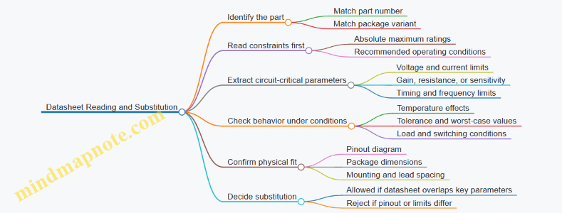
Part Substitution Rules That Prevent Silent Failures
Substitution is safe when the replacement satisfies every constraint your circuit depends on. A good rule is to compare minimum requirements to datasheet guarantees.
Rule 1: Never substitute across pinout differences. Even if the electrical specs look close, a different pin order can short power rails or invert signals.
Rule 2: Match voltage ratings with margin. For semiconductors, ensure the relevant breakdown rating exceeds your maximum stress. For capacitors, match both capacitance and voltage, and consider ripple current for switching supplies.
Rule 3: Match current capability and thermal limits. A transistor with higher current rating can still fail if its thermal resistance is worse for your mounting method.
Rule 4: Match the “mode” of operation. A part used as a linear amplifier must meet linear-region expectations, not just switching specs.
Rule 5: Match timing and frequency behavior. For RC timing, the resistor and capacitor values matter; for logic parts, propagation delay and input thresholds matter.
Example: Substituting a Resistor with a Different Tolerance
Suppose your circuit uses a 10 kΩ resistor as a voltage divider. If you substitute 10 kΩ ±1% for 10 kΩ ±5%, the divider ratio becomes more stable. That’s usually beneficial.
But if your circuit depends on a threshold crossing, tolerance affects whether the input stays above or below the threshold across temperature and supply variation. In that case, you should compute worst-case divider outputs using the tolerance values from the datasheets.
Example: Substituting a Regulator with a Similar-Looking Part
You find a regulator with the same package and output voltage. Before swapping, verify:
- Input voltage range includes your maximum input.
- Dropout at your load is low enough.
- Output current capability meets your load.
- Enable pin behavior matches your circuit.
- Quiescent current and thermal limits won’t overheat the regulator.
If any of these don’t match, the substitution may work on a bench test at room temperature but fail under your actual load or wiring conditions.
A Simple Substitution Checklist
Before you commit to a swap, confirm these in order:
- Pinout matches.
- Electrical limits cover your worst-case stresses.
- Key parameters match the circuit’s operating mode.
- Thermal behavior is compatible with your mounting.
- Tolerance and temperature effects won’t break thresholds.
This approach keeps substitutions from becoming guesswork, and it makes your builds easier to troubleshoot later—because you’ll know exactly which constraints you honored.
1.5 Building a Repeatable Workflow from Schematic to Verified Circuit
A repeatable workflow turns “it works on my breadboard” into “it works the same way every time.” The goal is not speed; it’s predictable outcomes with clear evidence at each step.
Start with a Build Plan That Matches the Schematic
Before touching parts, translate the schematic into a checklist.
- Create a net list: list each node name (VCC, GND, sensor_out, etc.) and what connects to it.
- Mark power domains: note which parts share the same supply rail and which are isolated.
- Identify measurement points: decide where you will probe to confirm behavior (input, output, reference voltage, and any control node).
Example: If you’re building a 5 V regulator plus an LED driver, your plan should include probing the regulator output, the LED driver input, and the LED current sense point (or the resistor voltage).
Assemble in Stages, Not in One Big Leap
Stage assembly reduces the number of unknowns.
- Power-only stage: build only the power path and any regulators.
- Signal path stage: add the first amplification or conditioning blocks.
- Load stage: connect the final output device like an LED, motor driver, or sensor.
Each stage ends with a verification step. If stage 1 fails, you don’t waste time debugging stage 3.
Verify Electrical Assumptions Early
Most beginner failures come from incorrect assumptions that could have been tested quickly.
- Continuity and shorts: confirm no accidental shorts between rails.
- Polarity checks: verify diode orientation, electrolytic capacitor polarity, and transistor pin mapping.
- Voltage expectations: compare measured voltages to what the schematic implies.
Example: For a divider that should produce 1.65 V from 3.3 V, measure the divider output before connecting it to an ADC. If it’s off by 20%, you’ll know the issue is resistor values or wiring, not the microcontroller.
Use a Consistent Measurement Routine
A routine prevents “probe roulette.”
- Define probe order: measure from input to output, left to right in the schematic.
- Record values with units: include volts, milliamps, and temperatures when relevant.
- Note conditions: whether the circuit is unloaded, lightly loaded, or fully loaded.
A simple table you can reuse:
| Node | Expected | Measured | Pass/Fail | Notes |
|---|---|---|---|---|
| VREG_OUT | 5.00 V | 4.86 V | Fail | Drop under load |
| LED_ANODE | 5.00 V | 5.00 V | Pass | — |
| LED_RES_V | 1.20 V | 0.95 V | Fail | Likely wrong resistor |
Confirm Function with a Minimal Stimulus
Instead of applying “real-world” inputs immediately, use minimal stimuli that isolate behavior.
- DC stimulus: apply a fixed input voltage to test biasing.
- Step stimulus: toggle a digital input to test timing and thresholds.
- Known load: use a resistor or dummy load before connecting a complex device.
Example: When testing a comparator or threshold detector, feed a slow ramp or a stepped voltage rather than a noisy sensor signal. Once thresholds are correct, you can add the sensor.
Document the Build Like a Lab Notebook
Documentation is part of verification, not an afterthought.
- Mark wiring changes: if you swap a resistor value, write it down immediately.
- Capture component IDs: record package type and any substitutions.
- Store screenshots or photos: take one photo of the full build and one of the measurement setup.
A good habit: label wires at both ends with the net name from the schematic. It saves time when you revisit the circuit later.
Mind Map: From Schematic to Verified Circuit
Example Workflow for a Simple LED Indicator Circuit
Assume the schematic includes a 5 V rail, a current-limiting resistor, and an NPN transistor switch.
- Power-only stage: build the 5 V rail and the resistor network; verify 5 V at the expected node.
- Polarity checks: confirm transistor orientation and LED direction.
- Signal path stage: connect the transistor base driver but keep the LED disconnected; measure base voltage and confirm it reaches the expected level.
- Load stage: connect the LED and measure the resistor voltage. If the resistor voltage is low, the LED current is low, which points to wiring, resistor value, or transistor saturation.
- Record results: write measured voltages and the observed LED behavior (on/off brightness under a known input).
Common Failure Points and How the Workflow Catches Them
- Wrong pinout: caught by polarity checks and early voltage expectations.
- Miswired nets: caught by continuity checks and net-name labeling.
- Incorrect resistor values: caught by measuring the voltage across the resistor before blaming the transistor.
- Load-dependent issues: caught by documenting load conditions and repeating measurements under the intended load.
A repeatable workflow is basically a chain of small proofs. Each proof narrows the search space, so the final “it works” is backed by measurements, not hope.
2. Core Circuit Building Blocks You Will Use Every Day
2.1 Resistors Capacitors and Inductors in Practical Circuits
Resistors, capacitors, and inductors are the “three knobs” of analog behavior. Resistors set current and voltage division, capacitors store charge and shape edges, and inductors resist changes in current. In practical bench projects, you use them together to control gain, timing, filtering, and stability—often without needing to memorize advanced theory.
Resistors: The Current and Voltage Shapers
A resistor follows Ohm’s law: \(V = I R\). In circuits, resistors appear in three common roles.
-
Current limiting and pull-ups/pull-downs: An LED needs a resistor to keep current within a safe range. If you have a 5 V supply and a 2.0 V LED drop, and you want about 10 mA, the resistor is \(R = (5-2)/0.01 = 300,\Omega\). A 330 \(\Omega\) part is a typical safe choice.
-
Voltage dividers: Two resistors split a voltage. If you need a reference for a comparator or ADC, choose divider values so the divider current is large enough to resist leakage effects but small enough to avoid wasting power. A useful rule of thumb is to keep divider current at least an order of magnitude higher than the input bias currents you’re dealing with.
-
Biasing and feedback: In amplifier stages, resistors define operating points and feedback ratios. The key practical habit is to verify the resulting currents and voltages with your multimeter before connecting sensitive parts.
Resistor Practicalities
Resistors are not perfectly constant. Tolerance affects thresholds, and temperature coefficient shifts values slightly. When you’re building something that depends on a precise trip point, measure the resistor with a multimeter and account for tolerance in your calculations.
Capacitors: Charge Storage and Timing
A capacitor stores charge: \(Q = C V\). The voltage across a capacitor cannot change instantly. That single sentence explains why capacitors smooth signals and create delays.
In time-domain behavior:
- Charging through a resistor follows an exponential curve with time constant \(\tau = R C\).
- After one \(\tau\), the capacitor reaches about 63% of its final voltage.
- After about 5\(\tau\), it’s effectively settled for most bench purposes.
Example: RC Delay for a Button
Suppose you want a “press-and-hold” delay before enabling an output. Use a resistor from the button to a capacitor, and a resistor from the capacitor to ground (or to a logic threshold reference). When the button is pressed, the capacitor charges; when released, it discharges. Choose \(R\) and \(C\) so \(\tau\) matches your desired delay scale. If you want roughly 0.5 s to reach near-threshold, pick \(\tau\) around 0.1 s to 0.2 s and then account for the threshold level you actually use.
Capacitor Practicalities
Capacitors have leakage and equivalent series resistance (ESR). For timing circuits, leakage matters mostly at high resistance values. For filtering power rails, ESR and ripple current ratings matter. If you see unexpected behavior, measure the capacitor voltage waveform with an oscilloscope—capacitors often reveal the truth quickly.
Inductors: Current Change Resistance
An inductor opposes changes in current. The voltage across an inductor is \(V = L \frac{dI}{dt}\). In steady DC, an ideal inductor acts like a wire; in changing conditions, it acts like a brake.
Example: Flyback Protection with an Inductor
When you switch an inductive load (like a relay coil), the current wants to keep flowing. If you don’t provide a path, the voltage can spike high enough to damage transistors. A flyback diode is common, but inductive energy also interacts with wiring inductance and supply impedance. The practical takeaway is to treat switching loops as physical objects: keep them short, and use the right protection topology.
Inductor Practicalities
Inductors have DC resistance (DCR) and saturate at high current. If a circuit “works on the bench” but fails under load, saturation is a frequent culprit. Measure coil resistance and verify current ratings against your expected peak current.
How They Work Together
Resistors set levels and currents, capacitors shape edges and filter noise, and inductors smooth current and resist rapid changes. When you combine them, you get predictable behaviors like low-pass filtering (resistor + capacitor) and resonant networks (resistor + capacitor + inductor).
Mind Map: Resistors Capacitors and Inductors
Bench Method: Verify Before You Trust
For any RC or RL timing circuit, measure the waveform at the capacitor or inductor node. Confirm the time constant scale, then confirm the threshold crossing that triggers your logic. This turns “the math says it should work” into “the circuit actually behaves the way we designed it,” which is the whole point of a bench.
2.2 Diodes and Rectifiers for Reliable Power Conversion
Power conversion is mostly about controlling where current is allowed to go. Diodes do that job with a simple rule: they conduct in one direction and block in the other. Rectifiers then use diode behavior to turn alternating current into a unidirectional output. In bench projects, this matters because “it powers up” is not the same as “it powers up predictably,” especially when loads change or ripple shows up.
Diode Fundamentals That Matter in Bench Builds
A diode’s key parameters are forward voltage drop, reverse leakage, and maximum ratings. The forward drop is not a fixed number; it depends on current and temperature. For beginners, the practical takeaway is to treat the diode drop as a budget item in your power calculations.
Reverse leakage is usually small at room temperature, but it can become noticeable in high-impedance circuits. Maximum ratings matter because a diode can fail short or open, and either outcome can confuse troubleshooting. Always check:
- Forward current rating versus your load current
- Reverse voltage rating versus the peak voltage across the diode
- Power dissipation based on forward drop and current
A diode also has a switching speed, but for typical rectifier frequencies in linear supplies and many bench adapters, the dominant effects are voltage drop and ripple.
Rectification Basics from Waveforms to Output
An AC source swings positive and negative. A rectifier forces the output to keep the same polarity by steering current through diodes.
Half-Wave Rectification
With one diode, only one half-cycle reaches the load. The output is pulsed DC with large ripple. This is simple, but it wastes power and stresses the supply with a pulsating current draw.
Full-Wave Rectification
Full-wave rectification uses both half-cycles, reducing ripple and improving efficiency. Two common approaches are:
- Center-tapped full-wave using two diodes
- Bridge rectifier using four diodes
A bridge is often easier for beginners because it works with a non-center-tapped transformer and still gives full-wave output.
Bridge Rectifier Behavior and the “Two Diodes” Reality
In a bridge, current always passes through two diodes during each half-cycle: one from the AC input to the positive output, and another from the negative output back to the other AC terminal. That means the effective forward drop is roughly two diode drops.
This is why bridge rectifiers often use Schottky diodes or low-drop silicon diodes when efficiency matters. For linear regulators, the extra drop reduces headroom, which can cause dropout at lower input voltages.
Filtering with Capacitors Without Getting Surprised
A capacitor across the load smooths the rectified waveform. It charges near the peaks and then discharges between peaks. The ripple voltage depends on load current, capacitance, and rectifier frequency.
A useful bench habit is to estimate ripple and verify that your regulator or downstream circuit can tolerate it. If ripple is too large, you may see unstable readings from sensors or noisy analog measurements.
Practical Design Workflow for Reliable Rectifiers
- Compute peak voltage from the transformer secondary RMS value: peak is about RMS × 1.414.
- Choose diode reverse voltage rating comfortably above the peak.
- Budget forward drops: half-wave uses one diode drop; bridge uses two.
- Estimate capacitor ripple using load current and rectification frequency.
- Check regulator headroom if you use a linear regulator after rectification.
Mind Map: Diodes and Rectifiers for Power Conversion
Example: Choosing Diodes for a 12 V RMS Transformer
Assume a transformer secondary of 12 V RMS.
- Peak voltage ≈ 12 × 1.414 ≈ 17 V.
- For a bridge, two diode drops reduce the capacitor-charged peak available to the load/regulator. If each diode drops about 0.7 V at your current, that’s about 1.4 V total.
- The capacitor will charge to roughly peak minus diode drops, minus any wiring losses. That gives a starting point for regulator headroom.
Now the diode reverse voltage rating should exceed the peak with margin. A common beginner mistake is using a diode rated just above the peak; in real builds, transformer regulation and transients can push higher. Pick a diode with a comfortably higher reverse voltage rating than the computed peak.
Example: Half-Wave vs Bridge Ripple Intuition
If you rectify with half-wave, the output pulses occur once per AC cycle. With full-wave, pulses occur twice per cycle. That means the capacitor sees more frequent recharge opportunities in full-wave, so ripple is typically smaller for the same capacitance and load.
A quick bench check is to measure ripple with a scope or even a multimeter on AC volts across the load capacitor. If the ripple is too high, increase capacitance (within diode and regulator limits) or switch to full-wave.
Common Bench Pitfalls and How to Avoid Them
- Underestimating diode drops: bridge circuits lose more voltage than half-wave.
- Ignoring regulator headroom: ripple and diode drops can push the regulator into dropout.
- Choosing diodes by current only: reverse voltage rating is equally important.
- Overlooking capacitor discharge behavior: large loads can cause ripple to rise sharply.
Rectifiers are simple circuits, but reliable power conversion comes from treating diode drops, ratings, and ripple as first-class design constraints rather than afterthoughts.
2.3 Transistors for Switching and Simple Amplification
Transistors are three-terminal devices that let you control a larger current with a smaller one. In beginner bench projects, the two most common jobs are switching (turning something on or off) and simple amplification (making a small signal bigger without adding much complexity).
Foundational Concepts for Transistor Behavior
A transistor has three terminals: base, collector, and emitter (for BJTs). For NPN BJTs, current flows from collector to emitter when the base is driven high enough. For PNP, the polarities flip.
Two operating regions matter most for switching:
- Cutoff: base-emitter is not forward biased, so collector current is near zero.
- Saturation: base-emitter is driven enough that the transistor behaves like a low-resistance path.
For amplification, you care about the active region, where the transistor behaves more like a controlled current source. The key idea is that the collector current changes with base current, but not in a perfectly linear way.
Switching with BJTs Using Clear Bench Rules
A practical switching design starts with a target load current and a safe base drive.
Step 1: Choose a Load and Target Current
Suppose you want an LED to turn on reliably from a 5 V control signal. If the LED plus resistor draws 20 mA, you want the transistor to sink about 20 mA when “on.”
Step 2: Pick a Base Resistor That Forces Saturation
A common beginner mistake is calculating base current using only transistor gain (β). Real transistors vary, and saturation requires extra base current. A good rule is to assume a conservative gain, such as using β = 10 for base-current sizing.
If the base-emitter drop is about 0.7 V for a BJT, then:
- Base resistor: \(R_B \approx (V_{in}-0.7)/I_B\)
- Base current: \(I_B \approx I_C/10\)
Step 3: Verify with a Quick Sanity Check
When saturated, the collector-emitter voltage is not zero; it might be around 0.1–0.3 V depending on current and device. That’s fine for LEDs and most small loads, but it matters for power dissipation.
Example: NPN Low-Side LED Switch
- Supply: 5 V
- LED current target: 20 mA
- Assume β-for-saturation: 10
- Base current target: 2 mA
- Base resistor: \(R_B \approx (5-0.7)/2mA \approx 2.15k\Omega\)
Use a standard value like 2.2 kΩ. If the LED is dim or doesn’t fully turn on, increase base drive (smaller resistor) rather than assuming the transistor is “wrong.”
Simple Amplification with BJTs Without Overpromising
Amplification is where you stop thinking in “on/off” terms and start thinking in “small changes.” A BJT amplifier usually uses a bias network so the transistor sits in the active region.
Biasing for Active Region
A basic common-emitter amplifier uses:
- A collector resistor to set current and convert current changes into voltage changes.
- An emitter resistor to stabilize operating point.
- A bias network to set base voltage.
The goal is to keep the transistor away from cutoff and saturation during the entire signal swing.
Small-Signal Reasoning
In active region, a small change in base current causes a larger change in collector current. That current change through the collector resistor creates a voltage change at the collector. The amplifier’s overall gain depends on resistor values and transistor behavior.
Example: Common-Emitter Voltage Amplifier Sketch
- Choose a collector resistor so the transistor has headroom.
- Add an emitter resistor for stability.
- Use a coupling capacitor to block DC while passing AC.
If your output clips at the top or bottom, it’s usually because the bias point is wrong or the input amplitude is too large.
Practical Design Mind Map
Mind Map: Transistor Switching and Amplification
Bench Checks That Prevent Most Problems
- Measure voltages, not vibes: confirm base-emitter is around 0.7 V when “on” for an NPN switch.
- Check saturation behavior: if the collector-emitter voltage is high, the transistor may not be fully saturated.
- Watch power: transistor dissipation is \(P \approx V_{CE} \times I_C\) in switching; in amplification it depends on signal swing.
- Use the right protection: for motors, solenoids, and relays, include a flyback diode across the inductive load.
Mini Case Study: Switching a Relay Coil
A relay coil is inductive, so turning it off creates a voltage spike. If you drive a relay coil with an NPN low-side switch, place a diode across the coil (cathode to the positive supply, anode to the transistor side for typical NPN low-side wiring). This lets the transistor switch safely without being punished by the coil’s stored energy.
When the relay turns on, the transistor should saturate so the coil sees near the supply voltage. When it turns off, the diode provides a path for current decay, preventing extreme voltage at the collector.
That’s the core pattern: choose a transistor that can handle the current, size the base to reach saturation, and add the protection your load demands.
2.4 Operational Amplifiers for Buffering and Basic Signal Conditioning
Operational amplifiers (op-amps) are voltage-controlled voltage amplifiers. In beginner bench work, their most useful trick is simple: they can take a high-impedance input signal and produce a low-impedance output that behaves nicely with the rest of your circuit. That’s buffering. They can also shape signals with a few resistors and capacitors, turning “messy” sensor outputs into signals your next stage can measure.
Core Ideas Before You Wire Anything
An op-amp has two inputs: the inverting input (−) and the non-inverting input (+). With negative feedback in place, the circuit tends to force the two input voltages to become equal. This is often summarized as a “virtual short” between inputs, but the practical takeaway is: feedback makes the input difference small, so the output adjusts to satisfy the resistor network.
Two more practical properties matter for buffering and conditioning:
- Input impedance: Ideally very high, so the op-amp doesn’t load your sensor or previous stage.
- Output impedance: Ideally very low, so the op-amp can drive the next circuit without the voltage collapsing.
Negative feedback is what makes these behaviors stable. If you remove feedback, the op-amp will usually saturate and rail hard, which is a great way to learn what “not connected correctly” looks like.
Buffering with Voltage Followers
The simplest buffer is the voltage follower: connect the output directly to the inverting input (−), and feed your signal into the non-inverting input (+). The op-amp then outputs nearly the same voltage as the input, while isolating the source from the load.
Why it works: the feedback forces the inverting input to track the non-inverting input, and the op-amp output supplies whatever current the load needs.
When it helps:
- You have a sensor with a high output impedance.
- You want to measure a node without disturbing it.
- You need to drive an ADC input or a filter network.
Example: A potentiometer feeding an ADC. Without buffering, the ADC’s input sampling current can cause the measured voltage to sag or jitter. With a voltage follower, the potentiometer sees a high impedance, and the ADC sees a low impedance.
Basic Signal Conditioning with Gain and Filtering
Once you add resistors, you can set gain and control bandwidth. Two common starting points are the inverting amplifier and the non-inverting amplifier.
Non-Inverting Amplifier for Simple Scaling
Feed the signal into (+). Use a resistor divider from output back to (−) to set gain. The gain is set by resistor ratios, so you can scale a sensor output into a convenient range.
Example: A temperature sensor output that varies from 0.2 V to 1.0 V. If your next stage expects roughly 0–3.3 V, you can choose gain so the top end fits without clipping.
Best practice: choose resistor values that keep input bias currents from creating noticeable offsets. If you use extremely large resistors, tiny bias currents can turn into measurable voltage errors.
Inverting Amplifier for Summing and Inversion
Feed the signal into (−) through an input resistor, and connect a feedback resistor from output to (−). The (+) input is usually tied to a reference voltage (often ground).
Example: You want to subtract an offset or combine two signals. An inverting stage can sum currents through multiple input resistors, producing an output proportional to the weighted sum.
Best practice: keep the input resistor values consistent and verify the sign. It’s easy to wire the network correctly and still get an inverted waveform.
Adding a Single-Pole Low-Pass Filter
For many sensors, noise is mostly high-frequency. A simple RC low-pass can smooth the signal. In an op-amp circuit, you can place a capacitor in the feedback path to create a controlled roll-off.
Example: A microphone preamp output that looks spiky on a scope. A low-pass filter reduces the spikes while preserving the slow envelope you care about.
Best practice: filter cutoff should be chosen relative to your signal bandwidth, not relative to your impatience. If you set the cutoff too low, you’ll “fix” noise by removing the useful parts.
Mind Map: Buffering and Conditioning
Bench Checks That Prevent “Why Is It Wrong?”
- Start with a known input: apply a steady voltage (or a slow ramp) and confirm the output moves in the expected direction.
- Check headroom: if your supply is 5 V single-supply, the output may not reach exactly 0 V or 5 V. If you see flat tops or bottoms, it’s clipping.
- Confirm stability: if you add capacitors, watch for ringing on a scope. A capacitor in the wrong place can turn a clean circuit into a tiny oscillator.
- Measure impedance effects: if you’re buffering, compare the source voltage before and after connecting the load. A good buffer keeps the source voltage nearly unchanged.
With these building blocks—voltage followers for isolation, gain stages for scaling, and simple RC filtering for noise—you can turn many raw sensor signals into something your measurements can trust.
2.5 Regulators and Reference Voltages for Stable Measurements
Stable measurements start with stable voltages. A regulator’s job is to make the supply less sensitive to changes in load current, input voltage, and temperature. A reference voltage’s job is to provide a known “yardstick” for measuring other voltages. In practice, you often need both: a regulator to feed your circuit, and a reference to interpret sensor or ADC readings.
What a Regulator Actually Fixes
A linear regulator reduces output variation by burning excess voltage as heat. It typically performs well when the input is only moderately higher than the output and the load current is within its safe range. Switching regulators are more efficient but can inject ripple and noise that may matter for analog measurements. Either way, you should treat the regulator as part of your measurement chain, not a background detail.
A useful mental model is: regulator output error comes from three places—input variation, load variation, and internal noise. Input variation is handled by the regulator’s control loop. Load variation is handled by output impedance and loop response. Internal noise shows up as a small voltage riding on the output, which can be amplified by your sensor front end or ADC.
Choosing Regulator Type for Bench Projects
For beginner bench circuits, linear regulators are often the simplest choice for clean rails like 3.3 V or 5 V when current is modest. If you’re powering a microcontroller plus a few sensors, a linear regulator plus good decoupling usually gives predictable results.
If you need higher efficiency or the input-to-output voltage difference is large, switching regulators become attractive. When you use one for analog work, you should plan for filtering and layout discipline so the ripple doesn’t masquerade as sensor signals.
Decoupling That Actually Helps
Decoupling capacitors are not decorative. Place a small ceramic capacitor close to the regulator output and another close to the load’s power pins. The small one handles fast transients; a larger one helps with slower changes. If your circuit includes an ADC or a sensitive amplifier, route the reference and analog supply carefully so capacitor currents don’t create voltage drops in shared traces.
A quick bench test: measure the regulator output with a multimeter while toggling a load (for example, turning an LED string on and off through a transistor). If the reading moves noticeably, your regulator or wiring needs attention before you trust any analog measurement.
Reference Voltages: The Yardstick Problem
An ADC converts an input voltage into a number by comparing it to a reference. If the reference moves, the ADC result moves even when the input is constant. That’s why reference stability matters more than many beginners expect.
There are three common reference approaches:
- Regulator-as-reference: using a regulated rail as the ADC reference. This works for rough measurements but couples ADC accuracy to load changes and regulator noise.
- Dedicated reference IC: a component designed to output a stable voltage with low noise and good temperature behavior.
- Reference divider from a stable source: using a stable higher voltage and a precision divider. This can be practical when you need a specific reference level, but resistor tolerance and temperature coefficients become your new enemy.
Practical Example: Measuring a Potentiometer Reliably
Suppose you want to read a potentiometer with an ADC. The potentiometer voltage depends on its supply and divider ratio. If you power the potentiometer from the same rail that the ADC uses, any rail sag becomes a measurement error.
A better approach is to:
- Regulate the supply feeding the potentiometer and ADC.
- Use a stable reference for the ADC.
- Add a small RC filter at the ADC input if the potentiometer wiper noise is significant.
Example reasoning: if your ADC reference is 3.300 V and it drifts by 10 mV due to regulator noise or load steps, that’s about 0.3% of full scale. On a 12-bit ADC, 0.3% corresponds to roughly 12 counts—enough to notice when you expect smooth readings.
Mind Map: Regulator and Reference Stability
Advanced Details That Still Fit on a Bench
Headroom matters for linear regulators. If the input falls too close to the output, the regulator may drop out, and your “stable” rail becomes a moving target. Always verify the minimum input voltage during your load conditions.
Load current limits matter. Many regulators have minimum load requirements for stable operation, especially in low-power modes. If you run a regulator with tiny loads, the output can behave oddly.
Reference buffering matters. Some ADCs expect the reference source to have low output impedance. If you use a reference IC or a divider, consider whether the ADC’s reference input needs buffering to avoid interaction.
Example: Quick Verification Workflow
- Power your circuit and measure the regulator output with a multimeter.
- Toggle a known load step and watch for output movement.
- Apply a known voltage to the ADC input (for example, from a stable divider or a bench supply set to a fixed value).
- Record ADC readings before and after load steps. If readings change, the reference or supply coupling is the culprit.
When this workflow is consistent, you can trust that changes in your ADC results come from the signal you’re measuring—not from the power system doing its own thing.
3. First Projects with Breadboards and Discrete Components
3.1 LED Indicators with Current Limiting and Test Points
LED indicator circuits look simple, but the “simple” part is mostly the wiring. The reliability part comes from controlling current, choosing the right resistor value, and making it easy to verify behavior without guessing.
Foundational Concepts for LED Indicators
An LED is a diode that emits light when forward-biased. Its brightness depends strongly on forward current, and its forward voltage depends on color and temperature. That means a fixed resistor is not optional if you want predictable results.
A basic indicator uses:
- A DC supply (often 5 V or 12 V)
- An LED
- A series resistor to limit current
- Optional test points so you can measure voltage and confirm polarity
Current Limiting with a Series Resistor
Use the resistor to absorb the “extra” voltage and set current.
- Find the LED forward voltage \( V_f \) from the datasheet (typical values: red ~2.0 V, green ~2.1–2.2 V, blue/white higher).
- Compute resistor value:
\[ R = \frac{V_{supply} - V_f}{I_{target}} \]
- Choose a standard resistor value close to the result.
- Pick a resistor with enough power rating: \[ P = I_{target}^2 \cdot R \]
Example: 5 V supply, red LED \(V_f = 2.0\text{ V}\), target current \(I = 10\text{ mA}\).
- \(R = (5 - 2)/0.01 = 300,\Omega\)
- Use \(330,\Omega\) for a slightly dimmer LED and extra safety.
Polarity and Wiring Checks
LEDs have polarity: the longer lead is typically the anode. If you reverse the LED, it won’t light, and the resistor won’t “fix” that. A quick continuity check with a multimeter helps prevent silent wiring mistakes.
Practical Build: One LED with Test Points
Build the circuit so you can measure:
- Supply voltage at the input
- Voltage across the LED
- Voltage across the resistor
- LED current indirectly (by measuring resistor voltage and using Ohm’s law)
Recommended Layout
- Place the resistor in series with the LED.
- Keep the loop area small to reduce noise pickup if you later add switching.
- Add test pads or header pins for the nodes: \(V_{in}\), \(V_{LED}\), and \(V_{R}\).
Node Voltage Reasoning
If the LED is on, you should see:
- \(V_{LED}\) near the LED forward voltage (often around 2 V for red)
- \(V_{R} = V_{in} - V_{LED}\)
- Current estimate: \(I \approx V_{R}/R\)
If the LED is off, measure anyway:
- If \(V_{in}\) is correct but \(V_{LED}\) is near 0 V, the LED may be reversed or open.
- If \(V_{in}\) is low, the supply wiring or regulator may be sagging under load.
Mind Map: LED Indicator Design Checklist
Example: 12 V Supply with a Green LED
Assume a green LED with \(V_f = 2.2\text{ V}\) and you want \(I = 8\text{ mA}\).
- \(R = (12 - 2.2)/0.008 = 1212.5,\Omega\)
- Choose 1.2 kΩ or 1.3 kΩ.
If you use 1.2 kΩ:
- Expected current \(I \approx (12 - 2.2)/1200 \approx 8.17\text{ mA}\)
- Resistor power \(P \approx I^2 R \approx (0.00817)^2 \cdot 1200 \approx 0.08\text{ W}\) Use at least a 0.25 W resistor for comfortable margin.
Test Point Strategy That Saves Time
Add three test points:
- Vin: confirms the supply is present.
- Vled: confirms the LED is forward-biased.
- Vr: lets you compute current without needing a current meter in series.
If you later build a multi-LED panel, keep the test point naming consistent across channels. That consistency turns troubleshooting into a repeatable routine instead of a guessing game.
Quick Troubleshooting Workflow
- Verify Vin at the Vin test point.
- If Vin is correct, check Vled.
- If Vled is near 0 V, suspect reversed LED or open circuit.
- If Vled is reasonable but the LED is dim, check resistor value and supply voltage under load.
- If Vr is unexpectedly high, current is likely lower than expected due to wrong resistor or a partially open connection.
This approach keeps the circuit “boring” in the best way: predictable current, measurable nodes, and fewer surprises when you probe it.
3.2 Button Debounce Circuits With Clean Digital Inputs
A pushbutton rarely produces a single, clean transition. Mechanical contacts bounce, creating multiple fast on/off edges that can look like several presses. Debouncing turns that messy reality into one reliable digital event.
What “Clean” Means for Digital Inputs
For a microcontroller or logic gate, “clean” usually means: when the button is pressed, the input becomes stable at a logic level within a short, known time, and stays there until release. The key is not eliminating bounce instantly, but ensuring the output changes only once per physical action.
Foundational Model of Button Behavior
Treat the button as two signals: the intended state and the contact waveform. During press or release, the contact waveform toggles for a few milliseconds. Your circuit’s job is to ignore those toggles.
A practical rule: if you sample faster than the bounce duration, you must filter. If you sample slower, you might miss the first stable level. Debounce designs handle this by either smoothing with time constants or by requiring consistent readings.
Mind Map: Debounce Design Choices
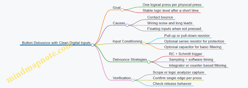
Hardware Debounce with RC Filtering and Schmitt Trigger
A simple and effective approach uses an RC network to slow the edge, then a Schmitt trigger input to create a decisive threshold crossing. The capacitor charges through a resistor; bounce wiggles the contact, but the threshold crossing happens only when the RC voltage has moved far enough.
How to choose values: start with an RC time constant in the range of a few milliseconds. If your button bounce is typically 5 ms, an RC that reaches the threshold in about 2–10 ms is a good starting point. Too small: bounce can still cross the threshold multiple times. Too large: the press feels sluggish.
Example circuit concept:
- Use a pull-up resistor to define the idle state.
- Add a series resistor and capacitor to ground to form an RC low-pass.
- Feed the node into a Schmitt trigger buffer or a microcontroller pin with built-in hysteresis.
Example: RC Debounce with a Schmitt Input
Assume a microcontroller pin with Schmitt trigger behavior, or an external buffer.
- Pull-up: 10 kΩ
- Series resistor: 1 kΩ (optional, helps limit current during transients)
- Capacitor: 100 nF
The RC time constant is roughly 10 kΩ × 100 nF = 1 ms, plus effects of the series resistor and input threshold. If you observe multiple edges, increase the capacitor (for example to 220 nF) or the pull-up (for example to 22 kΩ). If the button response feels delayed, reduce the capacitor.
Software Debounce with Consistent Sampling
If you already have a microcontroller, software debounce is often straightforward and flexible. The idea: sample the input repeatedly, and only accept a state change after it stays consistent for a minimum time.
Core logic:
- Read the raw button input.
- If it differs from the last stable state, start a timer.
- If the input remains different for the debounce interval, commit the new stable state.
- If it flips back, cancel the timer.
This approach naturally handles both press and release bounce.
Example: Edge-Detecting Debounce in Code
// Debounce parameters
const uint32_t DEBOUNCE_MS = 20;

bool stable = false;      // last committed state
bool lastRaw = false;     // last sampled raw state
uint32_t changeAt = 0;   // time when raw first changed

void updateButton(bool raw, uint32_t nowMs) {
  if (raw != lastRaw) {
    lastRaw = raw;
    changeAt = nowMs;
  }

  // Commit only after raw stays put long enough
  if (raw != stable && (nowMs - changeAt) >= DEBOUNCE_MS) {
    stable = raw;

    // Example: detect press event on rising edge
    if (stable) {
      // handlePress();
    }
  }
}
If your button uses pull-ups, “pressed” might correspond to a logic low. In that case, invert raw or adjust the event condition.
Advanced Detail: Preventing False Triggers
Even with debounce, two hardware issues can ruin your day:
- Floating inputs: always use a pull-up or pull-down so the pin has a defined idle level.
- Long wires and noise: a series resistor plus the RC filter (or input hysteresis) reduces the chance that fast noise spikes cross thresholds.
Verification Checklist
- Press and release the button while watching the input on a scope or logic analyzer.
- Confirm you get exactly one logical transition per action.
- Try both slow and fast presses; bounce patterns vary slightly.
- If you see multiple transitions, increase filtering time or the software debounce interval.
A good debounce design makes the button feel consistent, not necessarily instantaneous. The goal is predictable digital behavior that matches what your circuit expects.
3.3 Simple Audio Beeps With Transistors and Timing Networks
A “simple beep” is a controlled burst of sound: you turn a speaker or buzzer on for a short time, then turn it off. The cleanest beginner approach uses a transistor as a switch and a timing network that decides how long the on-time lasts.
Core Idea and Signal Flow
Start with a trigger input (like a pushbutton). That trigger charges or discharges a timing capacitor through a resistor network. When the capacitor voltage reaches a threshold, the transistor stage changes state and the beep ends. This approach keeps the timing mostly independent of the exact button press length.
A practical architecture is:
- Trigger: momentary switch to apply power to the timing network
- Timing network: resistor-capacitor (RC) that sets the beep duration
- Switching stage: NPN transistor that drives a buzzer
- Current limiting: resistor(s) to protect the transistor and set base current
Choosing the Transistor Stage
Use an NPN transistor as a low-side switch: emitter to ground, collector to the buzzer negative, buzzer positive to +V. The transistor turns on when base current flows.
For a typical small buzzer, you’ll likely need a base resistor that limits base current. A safe first pass is to pick a base resistor so base current is a few milliamps, not tens of milliamps. If you don’t know the buzzer current yet, measure it later with a multimeter in series.
Timing Network That Creates a Beep Burst
The simplest beep burst uses an RC network that produces a delayed turn-off or delayed turn-on. One common beginner-friendly method is:
- When the button is pressed, the RC charges quickly
- A second transistor stage or a logic threshold decides when to stop driving the buzzer
To keep this section focused and buildable with minimal parts, use a single-transistor “pulse shaping” approach with a capacitor that discharges through a resistor, causing the base drive to fade. The buzzer turns on strongly at first, then the base current drops as the capacitor voltage falls, reducing buzzer drive until it stops.
Component Selection and Practical Example
Example target: 0.2 s to 1 s beep duration.
- Pick a supply voltage, like 5 V.
- Choose the buzzer type. If it’s a passive piezo buzzer, it may need an oscillator; if it’s an active buzzer, it beeps when DC is applied.
- For an active buzzer, you can drive it directly with the transistor switch.
- Choose RC values using the rough time constant rule:
- Time constant τ = R × C
- Beep duration is often a few τ values depending on how the base current decays.
Start with C = 10 µF and R = 47 kΩ. That gives τ ≈ 0.47 s. If the beep is too long, reduce R; if too short, increase R or C.
Wiring and Build Steps
- Wire the buzzer to +V and transistor collector.
- Connect emitter to ground.
- Add a base resistor between the timing node and the transistor base.
- Place the RC capacitor so it charges when the button is pressed and then discharges through the resistor network.
- Add a diode across the buzzer if it’s an inductive load (motors/solenoids). For many active buzzers, a diode is still harmless, but verify polarity and behavior.
Quick Debugging Checklist
If you get no sound:
- Confirm the buzzer is an active type if you’re applying DC.
- Check transistor orientation and base resistor placement.
- Measure buzzer current; a buzzer that draws too much current can prevent proper switching.
If you get constant buzzing:
- The timing capacitor may not be discharging. Check the discharge resistor path.
- The base resistor may be too small, keeping the transistor on.
If the beep duration varies wildly:
- Ensure the button wiring doesn’t introduce intermittent contact resistance.
- Use a capacitor with reasonable tolerance; electrolytics can vary more than film capacitors.
Example Values That Usually Work
- Supply: 5 V
- Buzzer: active buzzer
- Transistor: common NPN like 2N2222 class
- Base resistor: 1 kΩ to 4.7 kΩ as a starting range
- Timing capacitor: 10 µF
- Timing resistor: 22 kΩ to 100 kΩ for roughly 0.2 s to 1 s beeps
Once the first build works, you can treat the RC pair as your “beep length knob” and keep the rest of the circuit stable. That separation of concerns is the main reason this design is beginner-friendly.
3.4 RC Timing Circuits for Delays and Pulse Generation
RC timing circuits use a resistor to control current and a capacitor to store charge. The capacitor voltage changes exponentially, which is why RC timing is so useful for predictable delays and simple pulse shaping. The key idea is that the capacitor does not “jump” to a new voltage; it moves gradually toward a target set by the supply and the circuit’s thresholds.
Core Concepts You Need First
An RC network has a time constant, τ = R·C. After one time constant, the capacitor reaches about 63% of the way from its starting voltage toward its final value (for charging), or falls to about 37% (for discharging). After about 5τ, the change is close enough to the final value for most bench work.
To make timing practical, you need a threshold. A logic input, a comparator, or a transistor base-emitter junction provides a switching threshold. The timing interval is the time it takes the capacitor voltage to cross that threshold.
Charging and Discharging Waveforms
For a capacitor charging from 0 V toward Vcc through R:
- \(Vc(t) = Vcc·(1 − e^{(−t/τ)})\)
For discharging from Vcc toward 0 V through R:
- \(Vc(t) = Vcc·e^{(−t/τ)}\)
In real circuits, you rarely measure the full exponential curve. Instead, you measure the time until a threshold is crossed, then choose R and C so that the threshold crossing happens where you want it.
Delay Using a Single Threshold
A common beginner-friendly delay uses a resistor-capacitor feeding a threshold device. For example, connect the RC node to a Schmitt-trigger input. When you apply power or a step, the Schmitt input switches only when the RC voltage passes its defined threshold. Because Schmitt inputs have hysteresis, the output won’t chatter when the capacitor voltage hovers near the threshold.
Practical bench rule: pick a target delay, estimate τ from the threshold crossing, then verify with a scope. If you don’t have a scope, a logic analyzer plus a multimeter can still confirm the timing.
Pulse Generation with RC and Thresholds
RC networks can also create pulses by charging and then quickly resetting the capacitor. The simplest pattern is:
- An input step starts charging.
- When the capacitor crosses the threshold, the output switches.
- A second event discharges or clamps the capacitor, ending the pulse.
This is the same “one threshold crossing” idea, but the circuit is arranged so the threshold is crossed for a limited time.
Mind Map: RC Timing Circuits
Example: Power-On Delay with a Schmitt Trigger
Suppose you want an output to stay low for about 2 seconds after power is applied. Choose a capacitor C = 10 µF. Then τ = R·C. If you start with R = 200 kΩ, τ = 200k·10µF = 2 seconds.
A threshold device will switch before or after 1τ depending on its threshold level. With a Schmitt-trigger input, you can expect a fairly repeatable crossing time because hysteresis prevents multiple transitions. On the bench, measure the capacitor node voltage and note when the output changes. If the output switches too early, increase R or C; if too late, reduce them.
Example: Single Pulse from a Button Press
A simple pulse can be made by charging an RC node when a button is pressed, then discharging it quickly when the button is released. Connect the RC node to a Schmitt input so the output produces a clean pulse width.
A practical wiring approach:
- Use a resistor R from Vcc to the RC node.
- Use a capacitor C from the RC node to ground.
- Use the button to connect the RC node to Vcc (or to start charging) and release to allow discharge through a defined path.
If you notice the pulse width depends too much on how fast you press, the fix is to ensure the capacitor charging and discharging paths are controlled by resistors, not by the button’s contact resistance.
Advanced Detail: Choosing R and C Without Surprises
- Capacitor leakage matters. Electrolytic capacitors can leak enough to shift timing, especially with large R values. If timing seems “off” at high resistance, try a different capacitor type or reduce R.
- Input loading changes effective C. The threshold device input adds capacitance. For most beginner circuits it’s small, but it can still shift timing when C is tiny.
- Too-large R slows edges. Slow RC edges can cause multiple threshold crossings if hysteresis is missing. Add hysteresis or buffer the signal.
- Too-small C increases current spikes. When the capacitor is near 0 V, charging current can be large. Use a resistor that limits current to a comfortable level for your supply and switch.
Quick Design Workflow
- Pick the timing interval you want.
- Choose a reasonable capacitor value (often in the 1 µF to 100 µF range for bench delays).
- Compute τ = R·C and start with R that makes τ close to your interval.
- Use a threshold device with hysteresis or a comparator with defined thresholds.
- Verify by measuring the RC node and the output switching time.
RC timing is simple in concept and precise in practice once you treat the threshold crossing as the real “timer.” The capacitor does the math; your threshold decides when the circuit counts the seconds.
3.5 Voltage Divider Measurements and Calibration With Multimeter Checks
A voltage divider is the simplest way to scale a higher voltage down into a range your multimeter or microcontroller can safely read. The divider is just two resistors in series, with the output taken from the junction. The key practical idea is that the divider’s “math voltage” assumes ideal conditions, while real measurements include resistor tolerance, meter loading, and wiring resistance. Calibration is how you turn the math into something you can trust.
Foundational Divider Math and What It Assumes
For resistors R1 (top) and R2 (bottom), with Vin applied across the series pair, the ideal output is:
Vout = Vin × R2 / (R1 + R2)
This assumes:
- Resistors are exactly their nominal values.
- The output node is not loaded by anything.
- Connections are clean and stable.
In real bench work, the multimeter is usually high impedance, so it loads the divider only slightly. Still, it’s worth checking because “slightly” can matter when you’re chasing accuracy.
Build a Divider You Can Measure Without Surprises
Use a breadboard or perfboard with short leads. Place R1 and R2 in series, then bring the junction to a test point. Before measuring, confirm polarity and that you’re not accidentally shorting the junction to either rail.
A practical best practice: label the node names on your wiring (Vin, Junction, GND). It sounds basic, but it prevents the most common calibration failure: measuring the wrong node with confidence.
Multimeter Measurement Strategy
Measure in two passes: first with no extra load, then with the divider connected to the intended measurement or input.
- No-load check
- Set the multimeter to DC volts.
- Measure Vin between Vin and GND.
- Measure Vout between Junction and GND.
- Compute the measured ratio: k_meas = Vout / Vin.
- Loading check If your divider output will feed a circuit input, measure again with that circuit connected. The input resistance (or any parallel path) effectively changes the divider.
If you don’t know the input resistance, you can still detect loading by comparing k_meas with and without the load.
Calibration Workflow That Stays Simple
Calibration means creating a correction you can apply consistently. You can do this with a single-point correction or a two-point linear check.
Single-point correction
- Pick a Vin value you can reproduce.
- Measure Vin and Vout.
- Compute k_meas.
- Use Vout ≈ k_meas × Vin for future readings.
This works well when the divider behaves linearly, which it does for resistive dividers.
Two-point check
- Measure at two different Vin values (for example, near the low end and near the high end of your expected range).
- Compute k_meas1 and k_meas2.
- If they match closely, a single k_meas is enough.
- If they differ, investigate loading, wiring issues, or meter range behavior.
Mind Map: Divider Measurement and Calibration
Example: Calibrating a 10 kΩ and 2.2 kΩ Divider
Suppose R1 = 10 kΩ and R2 = 2.2 kΩ. The ideal ratio is:
k_ideal = 2.2 / (10 + 2.2) = 0.1803
Now measure with a bench supply.
- Set Vin = 5.00 V.
- Measure Vin = 5.01 V (your supply may drift a bit).
- Measure Vout = 0.905 V.
- Compute k_meas = 0.905 / 5.01 = 0.1807.
That’s extremely close to ideal. For future readings, you can use:
Vout ≈ 0.1807 × Vin
If you later connect a circuit input and Vout drops to 0.870 V at the same Vin, the ratio becomes 0.1737. That tells you the input is loading the divider, so you either redesign (lower R values) or calibrate with the load attached.
Example: Detecting Wiring and Range Issues
If you see k_meas change wildly between two Vin settings, don’t immediately blame the resistors. Common causes include:
- Junction wire intermittently touching a rail.
- Measuring Vout with the meter leads swapped.
- Using a meter range that behaves differently due to resolution.
A quick sanity check: measure continuity from the junction to the intended resistor node, and re-measure Vout with the meter leads firmly seated.
Practical Calibration Notes That Prevent Rework
- Use the same wiring and measurement points during calibration and later use.
- Record k_meas with units-free ratio and note whether the load was connected.
- If you need repeatability, take a few readings and average; resistor noise and supply ripple can otherwise masquerade as “calibration error.”
Once you have a stable k_meas for your exact setup, voltage divider readings become predictable. The math gives you the starting point; the multimeter checks tell you what reality is doing on your bench.
4. Power Supply Projects and Bench Friendly Regulators
4.1 Creating a Clean 5 V Rail with a Linear Regulator
A “clean” 5 V rail is one that stays close to 5.00 V under changing load, and doesn’t inject extra noise into the circuits you’re building. A linear regulator is a good first choice because it trades extra heat for simplicity and low ripple. The goal is to choose the right regulator, wire it correctly, and verify performance with basic measurements.
Foundations You Need Before You Build
Start with three numbers: input voltage, load current, and allowable heat. If your input is higher than 5 V, the regulator must drop the difference as heat. For example, with 9 V input and a 5 V output, the regulator drops 4 V. At 200 mA load, that’s 0.8 W of heat (4 V × 0.2 A). If you expect 500 mA, the same drop becomes 2 W, which may require a heatsink and careful airflow.
Next, decide what “clean” means for your project. Digital logic usually tolerates some noise, but analog sensors and ADC measurements are more sensitive. In practice, you’ll improve cleanliness by using proper input/output capacitors, short wiring, and a stable ground reference.
Selecting a Linear Regulator
Pick a regulator with:
- Output accuracy close enough for your use (fixed 5 V regulators are convenient).
- Adequate current rating with margin.
- A dropout voltage low enough for your lowest input voltage.
Dropout matters because if the input falls near the regulator’s dropout, the output stops regulating. A quick check: if your input might sag to 6.5 V, and the regulator needs 1.0 V dropout at your load, you’re fine. If your input might sag to 5.8 V, you may not be.
The Wiring That Makes It Work
A linear regulator needs stable capacitors and a layout that avoids oscillation. Use a typical pattern:
- Input capacitor near the regulator input to handle sudden current draw.
- Output capacitor near the regulator output to maintain loop stability.
- A common ground point for the regulator and the load.
If your breadboard wiring is long, the added inductance and resistance can cause voltage dips and measurement confusion. Keep the regulator and capacitors physically close, and route power and ground as a pair.
Example Build: 9 V to 5 V at 200 mA
Use a fixed 5 V linear regulator rated for at least 300 mA, and plan for heat.
- Input: 9 V nominal.
- Load: 200 mA.
- Heat estimate: (9 − 5) × 0.2 = 0.8 W.
Choose capacitors that match the regulator’s datasheet recommendations. If you don’t have them, a common starting point is:
- Input capacitor: 10 µF to 47 µF electrolytic plus a small ceramic (0.1 µF) in parallel.
- Output capacitor: 10 µF to 47 µF electrolytic plus 0.1 µF ceramic.
The small ceramic helps with high-frequency stability; the larger electrolytic helps with slower load changes.
Mind Map: Clean 5 V Rail Design
Verification Steps That Catch Real Problems
-
Measure output voltage under load. Don’t measure at the regulator pin and assume the load sees the same voltage. Put the multimeter probes at the load’s power and ground.
-
Check for overheating. If the regulator case is too hot to touch comfortably after a few minutes, reduce load current, lower input voltage, or add a heatsink.
-
Look for ripple or oscillation. If you have an oscilloscope, observe output ripple and any high-frequency oscillation. Without one, you can still detect issues by watching for unstable readings or audible noise from nearby components.
Common Mistakes and Fixes
- Too much input voltage. Higher Vin increases heat and can reduce reliability. If you can, use a lower input like 7–9 V instead of 12 V.
- Capacitors far away. Long leads act like inductors, undermining stability. Move capacitors close to the regulator.
- Ground confusion. If the load ground returns through a different path than the regulator ground, you’ll measure “clean” voltage at the regulator while the load sees noise.
Quick Reference Example Settings
- For a 9 V input and 200 mA load: expect about 0.8 W dissipation.
- Use input and output capacitors near the regulator, including a 0.1 µF ceramic in parallel.
- Verify at the load, not just at the regulator.
With these steps, your 5 V rail becomes a dependable foundation for the rest of the bench projects—less mystery, fewer surprises, and measurements that match what the circuit actually experiences.
4.2 Building a Adjustable Bench Supply Using a Regulator Module
An adjustable bench supply is mostly about two things: predictable regulation and safe, repeatable wiring. A regulator module gives you the regulation part; your job is to feed it clean power, set the output correctly, and verify behavior under load.
Foundations: What You Are Building
A typical adjustable regulator module expects a higher input voltage than the output you want. It regulates down to a chosen output level, usually with a control knob or trim potentiometer. The module also needs proper grounding so the output voltage you measure is the same reference the regulator uses.
Start by deciding your target range. For many beginner projects, a practical goal is 1.2 V to 12 V (or 1.2 V to 24 V depending on the module). Then pick an input source that stays comfortably above the maximum output plus the module’s dropout voltage. If the input is too close to the output, regulation will collapse as soon as current demand rises.
Wiring Plan That Prevents Common Mistakes
Use a star-like grounding approach: connect the regulator module ground to a single bench ground point, then route measurement leads from that same point. If you share ground through random breadboard rails, you can end up measuring a voltage that includes wiring drops.
A clean wiring plan:
- Input positive to module input +
- Input negative to module input −
- Output positive to module output +
- Output negative to module output − and then to your bench ground
Add a fuse or current-limited protection on the input side. Many regulator modules are robust, but a shorted output can still turn into a “why is everything hot” lesson.
Setting the Output Voltage Safely
Before turning the knob, set up measurement:
- Multimeter in DC volts mode.
- Probe across the module output terminals.
- Keep the load disconnected at first.
- Power the module with the input supply.
- Adjust the trim knob slowly until you reach the desired output.
Now connect a load and re-check. The output should stay close to the set value. If it droops significantly, either the input is too low, the module is hitting current limits, or the load wiring is adding resistance.
Example: 5 V Rail for Digital Experiments
Goal: produce a stable 5.0 V rail for logic-level testing.
- Choose an input supply of at least 7 V if the module is a typical buck/linear design, or higher if the module requires more headroom.
- Set the module output to 5.0 V with no load.
- Add a modest load such as a small set of LEDs with resistors or a microcontroller board.
- Measure again at the output terminals and, if possible, at the load end.
If the load-end voltage is lower than the regulator output voltage, your wiring is the culprit. Shorten leads, increase conductor thickness, or add a thicker pair for power.
Example: 9 V Rail for Analog Prototypes
Goal: power an op-amp circuit that needs headroom for signal swings.
- Set output to 9.0 V.
- Use a load that draws a realistic current, not just a voltmeter reading.
- Watch for oscillation or instability if your circuit includes long wires and high-gain stages.
A simple mitigation is to place a small capacitor across the regulator output close to where the circuit connects. This reduces voltage dips caused by transient current draw.
Advanced Details That Matter in Real Builds
Current Limiting and Protection Behavior
If your regulator module includes current limiting, treat it as a feature to test your wiring, not as a substitute for a proper fuse. When current limiting engages, the output voltage may drop. That behavior is useful for diagnosing shorts: the supply “backs off” instead of instantly overheating.
Thermal Management
Linear regulator modules dissipate power as heat:
- Dissipation is roughly (input voltage − output voltage) × output current.
That means running from 12 V down to 5 V at 1 A can be a lot of heat. If your module is linear and you need higher current, reduce the input-output difference or use a buck-type module.
Measurement Discipline
Measure at the regulator output terminals for module verification. Then measure at the load for system verification. Those two readings tell you whether the problem is regulation or wiring.
Mind Map: Adjustable Regulator Bench Supply
Example: Quick Checklist Before You Power a Circuit
- Input voltage is safely above the maximum output plus headroom.
- Output is set with no load.
- Grounding is consistent and measured from the same reference.
- A fuse or current-limited input path is in place.
- You re-measure output after connecting the circuit.
A regulator module makes the supply adjustable, but your bench discipline makes it trustworthy. Once you follow the same wiring and measurement steps every time, debugging becomes much less mysterious.
4.3 Adding Overcurrent Protection with Fuses and Current Limiting
Overcurrent protection is the part of your bench build that keeps a small mistake from turning into a scorched component. The goal is simple: when current rises above what the circuit can safely handle, the protection device interrupts the fault quickly and predictably.
Foundational Concepts You Need Before Choosing Parts
Start with three numbers: the supply voltage, the maximum normal current, and the worst-case fault current. Normal current is what your circuit draws when everything is healthy. Fault current is what could flow if a wire shorts, a regulator fails, or a load is miswired.
A fuse is a sacrificial switch. It opens when current exceeds its rating for long enough to heat the fuse element. Current limiting is a way to restrict how much current can reach the fault in the first place, buying time for the fuse (or preventing nuisance blows).
A practical bench rule: use a fuse to protect the wiring and upstream supply, and use current limiting to protect sensitive parts like regulators, LEDs, sensors, and small transistors.
Fuses: Choosing the Right Type and Rating
Pick a fuse type that matches your environment. For bench projects, common choices include:
- Fast-acting (F): interrupts quickly for electronics where you want minimal energy during faults.
- Time-delay (T): tolerates short inrush currents, useful for loads with capacitors or motors.
Next, choose the fuse rating using a conservative approach:
- Estimate normal current at the highest expected load condition.
- Select a fuse with a current rating above that normal current so it doesn’t blow during typical operation.
- Ensure the fuse’s interrupt rating is high enough for the maximum fault current your supply can deliver.
If you skip the interrupt rating, the fuse might open, but not safely. On a bench supply with a lot of available current, this matters.
Current Limiting: Two Simple Methods That Work
Current limiting can be done with either a series element that limits current by design, or a protection circuit that reacts to overcurrent.
Method A: Series resistor or PTC
- A resistor limits current immediately, but it wastes power during normal operation.
- A PTC resettable fuse (polyfuse) increases resistance as it heats, then returns to normal after cooling.
Use a resistor when you want a fixed limit and can tolerate heat. Use a PTC when you want automatic reset and don’t mind a slower response.
Method B: Electronic current limiting with a regulator or dedicated IC Many bench-friendly regulator modules include current limiting. If you use one, treat it as current limiting and still add a fuse upstream for wiring protection.
Integrated Protection Strategy for a Linear Regulator Rail
A common beginner-friendly architecture is: input fuse → current limiting element → regulator → load.
- The fuse protects the input wiring and the upstream supply.
- The current limiter reduces fault energy and helps avoid repeated fuse blows.
- The regulator protects itself within its own limits, but it should not be your only protection.
Here’s a concrete example.
Example: Protecting a 5 V Regulator Feeding a Small Sensor Board
Assume:
- Supply: 12 V
- Normal load: 150 mA at 5 V
- Worst-case fault: output short to ground
Steps:
- Choose a fuse that won’t blow at 150 mA normal current. If the input current is roughly 12 V to 5 V conversion efficiency (say 80%), normal input current is about 0.15 A × (5/12) / 0.8 ≈ 0.078 A. Pick a fuse rating above that, such as 0.25 A, while still being fast enough to protect wiring.
- Add a current limiting element in series with the regulator input. A small resistor can limit short-circuit current, but it will drop voltage during normal operation. A better bench compromise is a PTC sized so it trips under fault current but stays stable during normal operation.
- Verify with a controlled test: power the circuit with the load disconnected first, then connect the load. Finally, simulate a short at the regulator output using a current-limited bench setup or a safe temporary jumper and confirm the fuse behavior.
Mind Map: Overcurrent Protection with Fuses and Current Limiting
Practical Wiring and Layout Details That Prevent “Mystery Failures”
Place the fuse as close as possible to the power entry. If the fuse is far away, the wire segment between the connector and the fuse can still overheat during a short.
Use appropriate wire gauge for the maximum current your protection could allow before it trips. Also, avoid putting the fuse in a place where it can be bypassed by a loose connector or a solder bridge.
Finally, label the fuse value on the enclosure or on the bench power lead. When you’re troubleshooting later, you’ll thank yourself for not playing component detective.
Quick Checklist for This Subsection
- Normal current estimated at worst-case load.
- Fuse type chosen for electronics behavior and inrush conditions.
- Fuse interrupt rating checked against supply capability.
- Current limiting added to reduce fault energy and protect sensitive parts.
- Fuse placed at the power entry with correct wiring gauge.
- Controlled fault test performed safely and repeatably.
4.4 Creating a Dual Rail Setup for Analog and Digital Experiments
A dual-rail bench setup keeps analog measurements stable while digital circuits do their noisy, switching thing nearby. The goal is simple: separate power paths so digital current spikes don’t modulate your analog reference or sensor bias.
Foundational Concept: What “Dual Rail” Really Means
A dual rail setup typically uses two regulated supplies derived from one source:
- Analog Rail: powers op-amps, sensor front ends, ADC reference buffers, and anything that cares about microvolts.
- Digital Rail: powers logic, microcontrollers, level shifters, and drivers.
Both rails can share a common ground, but you route currents so the analog ground doesn’t carry digital return spikes.
Step 1: Choose Voltages and Decide the Common Ground Strategy
Start by listing what each subsystem needs. Common beginner-friendly choices:
- Analog rail: 5 V (for many sensor modules) or 3.3 V (if your ADC and sensors are 3.3 V).
- Digital rail: 5 V or 3.3 V depending on your logic board.
Then decide grounding:
- If both rails are low voltage and you’re building on a bench, use a single ground node but implement star routing so digital return currents don’t flow through the analog measurement ground.
- If you’re using higher precision analog, consider a separate analog ground node that connects to digital ground at one controlled point.
Step 2: Build the Power Distribution with Filtering at the Right Places
Filtering is where most “it works on the breadboard” circuits become “it works on the bench.” Use a two-stage approach:
- Bulk decoupling near each rail entry to handle sudden current demand.
- Local high-frequency decoupling near each IC or module to handle fast edges.
A practical starting point per rail:
- At the rail entry: 10 µF to 47 µF electrolytic (or polymer) plus 0.1 µF ceramic.
- Near analog ICs: add 0.1 µF ceramic and optionally 1 nF to 10 nF if you see ringing.
- Near digital ICs: keep 0.1 µF ceramic close to each power pin; add 1 µF if the board has long traces.
If you use a regulator module, still add decoupling at the module output. Regulators are not magic; they just reduce the problem, not erase it.
Step 3: Add Isolation Without Creating Measurement Errors
Isolation can be done with either components or layout. For beginners, component isolation is easiest to reason about.
- Use a ferrite bead or small resistor between the analog rail and the digital rail only if you’re sure the analog current is modest.
- For a ferrite bead: it blocks high-frequency noise while allowing DC current.
- For a resistor: it forms an RC-like drop with decoupling capacitors; it can be fine for op-amp bias rails but watch voltage drop.
A good rule: isolate the rails, but keep the analog rail impedance low at the frequencies your analog circuit needs.
Step 4: Wire It Like You Mean It
Use a star point at the supply outputs:
- Run separate wires from the star point to the analog rail distribution and digital rail distribution.
- Route analog sensor returns directly back to the analog ground point.
- Route digital returns back to the digital ground point.
If you must share a ground plane, keep the analog front end physically separated from digital switching areas.
Mind Map: Dual Rail Architecture
Example: Dual Rail for a Sensor Plus Microcontroller
Assume a sensor front end uses an op-amp at 5 V, and a microcontroller runs at 3.3 V.
- Create two regulated outputs from your bench source: 5 V analog and 3.3 V digital.
- At each regulator output, place 10 µF + 0.1 µF close to the rail distribution node.
- For the op-amp board, add 0.1 µF at each op-amp power pin and keep the sensor ground return wired back to the analog ground star.
- For the microcontroller board, ensure its decoupling is present on the board and add a 1 µF near the rail entry if the wiring is long.
- If you observe ADC jitter when the microcontroller toggles GPIO, add a ferrite bead in series with the analog rail feed to the sensor board, then re-check stability.
Example: Verifying the Setup with Measurements
Use your multimeter and oscilloscope if available.
- Measure analog rail ripple while toggling digital outputs.
- Probe the analog ground near the sensor return and compare it to the digital ground near the microcontroller.
- If the analog ground moves when digital switches, your return paths are still mixing.
A dual rail setup is “correct” when analog readings remain consistent during digital activity, not when the schematic looks tidy.
Common Pitfalls and Fixes
- Pitfall: One long ground wire from everything back to the supply. Fix by star routing and shortening analog returns.
- Pitfall: Decoupling only at the regulator. Fix by adding local capacitors at the analog ICs and near digital power pins.
- Pitfall: Isolation that causes voltage sag. Fix by using ferrite beads instead of resistors, or reduce analog current draw.
When you treat power and ground as part of the circuit, not just “where electricity comes from,” your analog experiments stop behaving like they’re haunted.
4.5 Adding Reverse Polarity Protection and Robust Power Connectors
Reverse polarity is the bench equivalent of stepping on a LEGO: it happens fast, and it can ruin your day. The goal is not just to “survive” a mistake, but to fail in a predictable way while keeping normal operation low-loss and easy to debug.
Foundational Concepts for Safe Power
Start by defining what “reverse” means in your setup. In most bench builds, the risk is swapping the two DC leads, not shorting them. That means your protection should address both cases:
- Reverse polarity: + and − are swapped.
- Accidental short: the supply is connected correctly, but the circuit draws too much current.
A robust design uses layers: input protection first, then distribution, then per-module protection. This section focuses on the first layer and the connectors that make correct wiring more likely.
Reverse Polarity Protection Options
Option A: Series Diode with Indicator
A simple diode in series with the input blocks reverse voltage. Choose a diode with:
- Current rating above your expected maximum.
- Voltage drop you can tolerate (often 0.4–1.0 V depending on diode type).
For a 5 V rail, a standard diode can steal enough voltage to cause brownouts. If you use this approach, verify the minimum input voltage your regulator still needs.
Option B: Schottky Diode for Lower Drop
Schottky diodes reduce forward drop, which helps when you’re near regulator dropout limits. The tradeoff is higher leakage current, which usually matters only for very low-power circuits.
Option C: MOSFET “Ideal Diode” Style
A P-channel MOSFET (or an N-channel arrangement with a controller) can reduce loss dramatically. The key idea is that the MOSFET is oriented so it turns on for correct polarity and turns off for reverse polarity.
When you implement this, pay attention to:
- Gate drive: the gate must see the right voltage relative to the source.
- Body diode behavior: some MOSFET arrangements still allow a path in one direction unless you use the correct topology.
Option D: Fuse Plus Protection
A fuse doesn’t stop reverse polarity by itself, but it prevents a reverse event from turning into a smoke event. Pair the fuse with one of the reverse-blocking methods above so the fuse handles shorts and the polarity device handles swaps.
Robust Power Connectors That Reduce Mistakes
Connectors are part of the circuit. A connector that allows easy miswiring is like leaving the safety off a tool.
Use these practices:
- Keyed connectors when possible so physical orientation prevents reversal.
- Consistent pinout across your bench modules.
- Color coding that matches your wiring convention, but don’t rely on color alone.
- Strain relief so tugging doesn’t loosen a conductor and create intermittent faults.
For bench work, consider a connector system where the mating plug is polarized. If you must use unkeyed headers, add a mechanical rule: one side always connects to the same rail, and the harness is built once and never “reversed for convenience.”
Systematic Wiring and Verification Workflow
- Plan the current path: input connector → protection → fuse → distribution rail → module.
- Measure voltage drop across your protection in normal operation.
- Test reverse polarity with a current-limited supply or a bench supply set to a safe current limit.
- Confirm fuse behavior by verifying the fuse rating matches your worst-case short current.
A good test is to intentionally swap the leads while watching whether the protection blocks power without drawing excessive current.
Example: Diode Protection with Fuse and Test Points
Below is a practical pattern for a simple DC input. It blocks reverse polarity and limits damage from shorts.
[DC Input Connector]
        |
     [Fuse]
        |
   [Reverse-Blocking Diode]
        |
   +V Rail to Modules
   -V Rail to Modules

Add test points:
TP+ before diode
TP+out after diode
TP- reference
Use TP+ and TP+out to quickly see whether the diode is conducting. If TP+out stays near zero during a reverse test, the protection is doing its job.
Mind Map: Reverse Polarity and Connector Robustness
Practical Design Checks Before You Build
- Voltage budget: ensure your regulator still works with the protection’s forward drop.
- Thermal budget: if you use a diode, confirm it won’t overheat at maximum current.
- Connector integrity: verify the connector mates firmly and doesn’t wiggle under light tug.
- Labeling: mark the rails on the harness and on the module so the next person (including future-you) doesn’t have to guess.
When these pieces work together, reverse polarity becomes a controlled event: the circuit stays off, the fuse doesn’t instantly become a one-time story, and the correct wiring is obvious from the hardware itself.
5. Sensor Interface Projects with Analog Front Ends
5.1 Reading Potentiometers and Light Sensors with Proper Scaling
When you read a potentiometer or a light sensor, you’re really doing two jobs: converting an analog voltage into a number, and then converting that number into a meaningful unit. The first job is electrical; the second is math plus calibration discipline. If you do both carefully, your readings stay stable and your controller logic stops acting like it’s guessing.
Foundational Signal Model
Most beginner bench setups use a voltage divider feeding an ADC input. The ADC measures voltage relative to a reference, producing a code from 0 to 2^N − 1.
- Potentiometer: a variable divider that maps knob position to voltage.
- Light sensor: often a photoresistor (LDR) or photodiode module that maps light level to voltage, usually through a divider or amplifier.
A key idea: the ADC does not know “brightness” or “knob position.” It only sees voltage.
Voltage Divider Basics That Matter
A divider has two resistances: Rtop from the supply to the node, and Rbot from the node to ground. The node voltage is:
- Vnode = Vsupply × Rbot / (Rtop + Rbot)
For a potentiometer used as Rbot, turning the knob changes Rbot, which changes Vnode. For an LDR, changing light changes Rldr, which changes Vnode in the same divider equation.
Choosing Divider Values
If Rtop and Rbot are wildly mismatched across the expected range, the node voltage will barely move for most of the range, and your ADC will waste resolution. A practical rule: pick values so that Vnode spans a useful portion of the ADC range (not just a tiny sliver).
ADC Scaling from Codes to Volts
For an N-bit ADC with reference Vref, the conversion is:
- code = round((Vnode / Vref) × (2^N − 1))
- Vnode = (code / (2^N − 1)) × Vref
Use the same Vref you actually have. If your board’s “5 V” supply is really 4.86 V, pretending it’s 5.00 V creates systematic error.
Scaling Volts to Meaningful Units
Potentiometer as Position
If the potentiometer is wired as a divider from Vs to ground, you can map the measured voltage to a normalized position:
- position = Vnode / Vsupply
If you want a 0–100% scale, multiply by 100. If you want degrees, you need the mechanical travel and any dead zones.
Light Sensor as Brightness Proxy
For an LDR divider, the relationship between light and resistance is nonlinear, so “brightness” is usually a proxy. You can still scale readings in a useful way:
- Use a normalized scale between two measured conditions.
- Optionally apply a curve fit later if you need better linearity.
A simple normalized brightness metric:
- brightness = (Vnode − Vdark) / (Vbright − Vdark)
Clamp to 0–1 to avoid negative values when the sensor is darker than your baseline.
Calibration Workflow That Doesn’t Drift into Chaos
- Measure Vsupply and Vref (or at least Vsupply if Vref is tied to it).
- Record ADC codes at known endpoints.
- Convert endpoints to volts using the ADC scaling.
- Compute mapping parameters for your chosen unit.
For potentiometers, endpoints are often “knob fully one way” and “fully the other way.” For LDRs, endpoints are “dark” and “bright” under your actual bench lighting.
Mind Map: Proper Scaling Pipeline
Example: Potentiometer to Percent
Assume:
- N = 10 (0–1023)
- Vref = 5.00 V
- ADC code = 512
Vnode = (512 / 1023) × 5.00 ≈ 2.50 V
position = Vnode / Vsupply ≈ 2.50 / 5.00 = 0.50
percent ≈ 50%
If your measured Vsupply is 4.86 V, redo the percent using 4.86 V to keep the endpoints honest.
Example: LDR Brightness Proxy
Assume you measure:
- Vdark = 0.62 V
- Vbright = 3.90 V
Now you read Vnode = 2.20 V.
brightness = (2.20 − 0.62) / (3.90 − 0.62) ≈ 0.55
Clamp to 0–1 if needed. This gives you a stable number that tracks light changes even though the underlying physics is nonlinear.
Practical Checks Before You Trust the Numbers
- Monotonicity: as you turn the potentiometer or increase light, the scaled value should move in the same direction every time.
- Endpoint sanity: fully one side should land near 0% and fully the other near 100% for the potentiometer.
- Noise behavior: if readings jump wildly, add a small RC filter at the ADC input or average multiple samples.
Proper scaling is mostly about respecting the chain: divider physics → ADC voltage → conversion math → calibrated meaning. Once that chain is consistent, your bench projects stop surprising you in the most avoidable ways.
5.2 Conditioning Thermistor Signals with Bias Networks
Thermistors change resistance with temperature, but most beginner circuits expect a voltage that moves in a predictable direction. A bias network turns the resistance change into a measurable voltage, while also setting the measurement range and the noise behavior.
What a Bias Network Must Do
A bias network should:
- Convert resistance change into a voltage with enough slope to measure temperature.
- Keep the thermistor within its intended operating current so self-heating stays small.
- Match the rest of your circuit’s input range, whether you use a multimeter, ADC, or comparator.
A good starting point is a voltage divider: one fixed resistor and the thermistor. The divider output is then read by your instrument.
Voltage Divider Fundamentals
Assume a thermistor resistance \(R_T\) and a fixed resistor \(R_F\). With a supply \(V_{S}\), the divider output at the junction is:
- If \(R_F\) is on top: \(V_{OUT}=V_S\cdot\frac{R_T}{R_F+R_T}\)
- If \(R_F\) is on bottom: \(V_{OUT}=V_S\cdot\frac{R_F}{R_F+R_T}\)
Choosing which side the thermistor sits on flips the direction of the voltage change. That matters when you want “higher temperature equals higher voltage” without extra inversion.
Choosing the Fixed Resistor for Useful Sensitivity
Sensitivity is about how much \(V_{OUT}\) changes per degree. In a divider, the slope is strongest when \(R_F\) is near \(R_T\) in the middle of your temperature range. Practical method:
- Pick a target midpoint temperature \(T_{MID}\).
- Look up \(R_T\) at \(T_{MID}\) from the thermistor’s datasheet.
- Set \(R_F\approx R_T(T_{MID})\).
If you choose \(R_F\) far away, the output becomes “stuck” near one rail and small temperature changes won’t move the voltage much.
Self-Heating Control
Thermistors heat themselves when current flows through them. The power is \(P=I^2R_T\). With a divider, the thermistor current is roughly \(I\approx\frac{V_S}{R_F+R_T}\). To reduce self-heating:
- Use the lowest supply voltage that still gives good measurement resolution.
- Prefer larger resistor values if your ADC input can handle the resulting source impedance.
- Avoid continuous high excitation if you can sample briefly.
A quick sanity check: if your measured temperature rises when the circuit is powered and then slowly settles, self-heating is likely.
Divider Output Conditioning for ADC Inputs
Many microcontroller ADCs have input impedance limits and benefit from a stable source impedance. If you use a divider with large resistors, the ADC’s sampling capacitor may not charge fully during the conversion window.
Two common fixes:
- Lower \(R_F\) and \(R_T\) values while keeping self-heating in check.
- Add a buffer amplifier or a small RC filter at the ADC pin.
A simple RC filter is often enough: place a small capacitor from ADC input to ground. This averages noise, but keep the RC time constant compatible with your sampling rate.
Example: 10 kΩ Thermistor Divider on 3.3 V
Suppose your thermistor is nominally 10 kΩ at 25°C and you care about roughly 10°C to 40°C. Start with \(R_F=10\text{ kΩ}\) and a 3.3 V supply.
- At 25°C, \(R_T\approx R_F\), so \(V_{OUT}\approx 1.65\text{ V}\).
- At colder temperatures, \(R_T\) increases or decreases depending on thermistor type. For an NTC thermistor, resistance increases when colder, so \(V_{OUT}\) moves toward the rail set by the divider orientation.
If your ADC reference is 3.3 V and you use a 12-bit ADC, each count is about 0.8 mV. That’s usually enough to see temperature changes, especially if you chose \(R_F\) near the midpoint.
Mind Map: Bias Network Design Flow
Example: Adding an RC Filter Without Breaking Measurements
If you see noisy readings, add a capacitor \(C\) from the divider output to ground before the ADC pin. Start small, like 0.1 µF to 1 µF, then verify that your readings settle quickly enough for your sampling interval. If you sample once per second, a larger capacitor is usually fine; if you sample rapidly, keep \(C\) smaller.
Calibration That Matches the Divider Reality
Even with a good \(R_F\), real thermistors vary. Calibration can be simple:
- Measure \(V_{OUT}\) at two or three stable temperatures.
- Convert each \(V_{OUT}\) back to \(R_T\) using the divider equation.
- Use the thermistor model or a lookup table to map \(R_T\) to temperature.
This keeps the bias network’s role clear: it provides a consistent electrical translation, and calibration corrects the remaining mismatch between ideal math and real parts.
5.3 Measuring Temperature with LM35 Style Sensors and Calibration
LM35 style sensors output a voltage proportional to temperature, typically 10 mV per °C. That simple relationship is great for beginners, but it also means your measurement chain matters: supply voltage, wiring resistance, ADC reference, and calibration choices all show up as real errors. The goal is to turn “volts” into “°C” with predictable accuracy.
Foundational Concepts and Signal Path
Start by mapping the signal path end to end:
- Sensor temperature changes the sensor’s internal output.
- The sensor’s output voltage travels through wires to your measurement point.
- Your ADC or multimeter measures that voltage.
- You convert voltage to temperature using the sensor’s scale factor.
- You optionally correct systematic error using calibration.
For an LM35 style sensor, the ideal equation is:
- Temperature in °C = (Measured_Volts) / 0.010
In practice, you rarely measure the “ideal” voltage. If your ADC reference is off by 2%, your temperature result will be off by about 2% too. If your wiring adds noise, the reading will jitter.
Wiring Practices That Prevent Common Errors
Use a stable supply and keep the sensor wiring tidy.
- Power: Feed the sensor from the same regulated rail you use for your ADC reference when possible.
- Grounding: Use a common ground point for sensor output measurement and ADC reference.
- Decoupling: Place a small capacitor (for example 0.1 µF) close to the sensor between V+ and GND to reduce supply ripple effects.
- Shielding: If you run long wires near switching signals, twist the sensor output with ground to reduce pickup.
A quick sanity check: measure the sensor output at room temperature before connecting it to any controller. If the voltage is wildly outside the expected range, stop and fix wiring or power.
Measurement Setup with a Multimeter or ADC
With a multimeter, you can directly read voltage and compute temperature. With an ADC, you convert ADC counts to volts first.
Example using an ADC:
- Suppose your ADC reference is 3.300 V.
- ADC reading is 2048 counts out of 4096.
- Measured_Volts = 2048/4096 * 3.300 = 1.650 V.
- Temperature = 1.650 / 0.010 = 165 °C.
If that number seems too high for your environment, the issue is usually reference voltage, scaling, or wiring polarity—not the sensor.
Calibration Strategy That Actually Helps
Calibration corrects systematic error. Two common sources are:
- Scale error: the sensor’s mV/°C differs slightly from the nominal 10 mV/°C.
- Offset error: the sensor output at 0 °C is not exactly 0 V.
A practical two-point calibration uses two known temperatures and fits a line:
- T = a * V + b
Where:
- a captures the effective mV/°C scale
- b captures offset
Procedure:
- Choose two temperatures you can reproduce reliably (for example, near 20 °C and near 50 °C).
- Let the sensor settle at each temperature until readings stabilize.
- Record V1 at T1 and V2 at T2.
- Compute:
- a = (T2 - T1) / (V2 - V1)
- b = T1 - a * V1
- Use T = a * V + b for subsequent measurements.
If you only do one-point calibration, you can correct offset but not scale. Two points generally give noticeably better results for beginners.
Mind Map: Temperature Measurement and Calibration
Example: Two-Point Calibration with Real Numbers
Assume you measure:
- At T1 = 20.0 °C, V1 = 0.206 V
- At T2 = 50.0 °C, V2 = 0.506 V
Compute:
- a = (50.0 - 20.0) / (0.506 - 0.206) = 30.0 / 0.300 = 100 °C/V
- b = 20.0 - 100 * 0.206 = 20.0 - 20.6 = -0.6 °C
So your calibrated formula is:
- T = 100 * V - 0.6
If later you measure V = 0.350 V:
- T = 100 * 0.350 - 0.6 = 34.4 °C
Notice how the correction shifts the result slightly compared to the ideal T = V/0.010 = 35.0 °C. That’s the point: calibration turns “close” into “consistent.”
Practical Tips for Stable Readings
- Settling time: After moving the sensor or changing its environment, wait for the voltage to stop drifting.
- Averaging: Take multiple samples and average to reduce noise; don’t average across a temperature change.
- Plausibility checks: If computed temperature jumps by tens of degrees while nothing changed, suspect wiring or reference issues.
With careful wiring, correct voltage-to-count conversion, and a simple two-point fit, an LM35 style sensor becomes a dependable temperature input for bench experiments—no mystery, just math and good habits.
5.4 Interfacing Microphones and Piezo Sensors with Gain Control
Microphones and piezo sensors both turn motion into voltage, but they do it in different ways. A typical electret microphone outputs a small analog signal that needs biasing and amplification. A piezo element outputs a voltage that can be large for a brief impact, but it is also high-impedance and can look “spiky” to the next stage. Gain control is how you make those signals land in a predictable voltage range for your ADC or comparator.
Signal Types and What They Imply
Start by identifying the sensor’s output behavior.
- Electret microphone modules usually include an internal preamp and output a low-impedance analog signal (often centered around a mid-supply bias). Your job is mostly to set overall gain and filter noise.
- Bare piezo elements behave like a voltage source in series with a capacitor. They can produce high voltages with sharp edges, so you need input protection, a defined load, and often a way to tame the spikes.
A practical rule: if the sensor’s datasheet says “high impedance” or shows an equivalent capacitance, treat it like a capacitor you’re measuring through a resistive path.
Gain Control Architecture
A reliable beginner-friendly architecture is a three-block chain:
- Input conditioning: biasing, protection, and impedance matching.
- Gain stage: non-inverting amplifier or a simple op-amp stage.
- Output shaping: filtering and level shifting so the ADC sees a stable range.
For both sensor types, you want to avoid saturating the amplifier. Saturation is not just “wrong amplitude”; it also destroys waveform shape and makes debugging harder.
Mind Map: Microphone and Piezo Gain Control
Electret Microphone Gain Control Example
Assume you have a microphone module that outputs an analog voltage centered at Vref = 2.5 V (for a 5 V system). You want a gain that makes speech-like peaks fit within the ADC range.
Step 1: Choose a gain target. If your ADC is 0–5 V and you expect about ±50 mV around Vref from the module, a gain of 20 gives ±1 V swings, which is usually safe.
Step 2: Build a non-inverting amplifier. Use an op-amp powered from 5 V (or ensure it can handle your supply). Set gain with the resistor ratio:
- Gain = 1 + (Rf / Rg)
Pick Rg = 10 kΩ and Rf = 190 kΩ for gain ≈ 20.
Step 3: Add a low-pass filter. A simple RC at the op-amp output (or in the feedback path) reduces high-frequency noise. For example, choose a cutoff around a few kHz if you’re sampling audio-like signals.
Step 4: Verify headroom. Tap the microphone lightly and watch the op-amp output. If it hits the rails, reduce gain or add attenuation.
Piezo Sensor Gain Control Example
A piezo element can generate a sharp voltage spike. If you connect it directly to an op-amp input, the input can be driven beyond rails or behave unpredictably due to the high source impedance.
Step 1: Define a safe input path. Use a series resistor (for current limiting) and clamp diodes to the rails (or to the op-amp input protection network if present). This keeps the op-amp from seeing out-of-range voltages.
Step 2: Provide a discharge path. Add a resistor from the piezo signal node to ground (or to a bias reference). This forms a load that reduces floating behavior and controls how quickly the piezo “rings” down.
Step 3: Use a gain stage that tolerates transients. A non-inverting amplifier works, but you must consider that the input is AC-like and spiky. Keep gain moderate at first.
Step 4: Shape the output. Add a low-pass filter to smooth the spikes into something your ADC can sample meaningfully. If you need “impact detection,” you can also follow the amplifier with a rectifier-and-filter approach, but for this section focus on linear gain plus filtering.
Practical Gain Tuning Workflow
- Start with low gain and confirm the output stays within your ADC range.
- Increase gain gradually while monitoring clipping on peaks.
- Adjust filtering last so you don’t confuse “too much gain” with “too much noise.”
- Use a repeatable stimulus: speak at a consistent distance for microphones, and tap the piezo with the same force and location.
Common Pitfalls and Fixes
- Ignoring bias for AC signals: if your sensor output is centered at mid-supply, your amplifier must preserve that reference.
- Too much gain with no headroom: clipping makes waveforms look “busy” and hides the real problem.
- Direct piezo connection: high impedance plus spikes equals unpredictable behavior; always include a load and protection.
- No filtering: the ADC samples noise and spikes, which makes gain tuning feel inconsistent.
With these pieces in place—conditioning, a controlled gain stage, and output shaping—you can treat both microphones and piezo sensors as predictable inputs rather than mystery voltage generators.
5.5 Filtering Noisy Sensor Signals with RC and Active Filters
Noise shows up as unwanted variation in a sensor’s output, and filtering is how you trade a little speed for cleaner measurements. The key is to filter at the right place: before a signal reaches a sensitive ADC input, and with component values chosen from the noise’s time scale.
Start with Signal and Noise Time Scales
Begin by identifying what you’re trying to measure. If your sensor changes slowly (temperature, light level), a modest low-pass filter is usually appropriate. If you need fast edges (switching, vibration), filtering must be gentler or targeted, because heavy filtering smears timing.
A practical way to reason about RC filters is to compare the filter’s cutoff frequency to the signal’s bandwidth. For a first-order RC low-pass, the cutoff frequency is:
- f_c = 1 / (2πRC)
Signals with frequency well below f_c pass with little attenuation. Signals well above f_c are reduced, with the attenuation increasing at 20 dB per decade for each pole.
RC Low-Pass Filters That Behave Predictably
A basic RC low-pass uses a resistor in series and a capacitor to ground. For sensor interfaces, the resistor often sits between the sensor output and the ADC input, while the capacitor shunts high-frequency noise to ground.
Best practice: choose R so the capacitor can charge quickly enough for your measurement rate, but not so small that it loads the sensor heavily. If the sensor is a voltage source with low output impedance, you can use a larger R without issues.
Example: Suppose a light sensor output is noisy due to switching power supplies around it. You want to smooth variations faster than about 10 Hz, but keep changes slower than that. Pick f_c ≈ 10 Hz.
- Choose C = 10 µF
- Then R ≈ 1 / (2π f_c C) ≈ 1 / (2π·10·10e-6) ≈ 1.6 kΩ
This yields a time constant τ = RC ≈ 16 ms, meaning the output approaches a new value with a few time constants. If you sample every 20–50 ms, the filter will settle enough to be useful.
Avoiding ADC Loading and Hidden Time Constants
Many ADC inputs are not infinite impedance. If you add an RC filter but ignore the ADC’s input capacitance, you may create a second, unintended pole. That can shift cutoff frequency and cause extra settling time.
Best practice: treat the ADC input as a small capacitor to ground. If you know the ADC input capacitance (or can measure settling), ensure the RC filter’s resistor is not so large that the ADC cannot settle within your sampling window.
A simple rule of thumb is to keep the RC resistor modest when sampling quickly, or buffer the signal with an op-amp.
Active Low-Pass Filters for Better Control
Active filters use an op-amp to provide gain or buffering while filtering. The advantage is that the op-amp isolates the filter network from the ADC input, and you can set cutoff more precisely.
A common choice is a single-pole active low-pass: an op-amp buffer or non-inverting amplifier with an RC network in the feedback path or at the input.
Example: You have a thermistor divider feeding an ADC. The divider is high impedance, and the ADC sampling causes jitter. Use an op-amp buffer with a low-pass at the op-amp input.
- Put R_f in series with the sensor output
- Add C_f from the op-amp input node to ground
- Configure the op-amp as a buffer (gain of 1) so the ADC sees low output impedance
This keeps the RC cutoff where you designed it and prevents the ADC from stealing charge from the capacitor.
Two-Pole Filtering with RC and Op-Amp Stages
If one pole is not enough, a two-pole filter reduces noise more strongly. A two-pole low-pass can be built by cascading two single-pole stages (each with its own RC cutoff), or by using a standard second-order topology.
Cascaded RC stages:
- Stage 1: f_c1
- Stage 2: f_c2
If both are equal (f_c1 = f_c2), the overall response rolls off faster than a single pole. The tradeoff is slower settling and more careful choice of sampling timing.
Best practice: when cascading, keep each stage’s resistor reasonable and ensure the op-amp can drive the next stage without saturating.
Mind Map: Choosing and Implementing Filters
Quick Design Workflow That Doesn’t Get Lost
- Estimate the signal’s useful bandwidth from how fast the physical quantity changes.
- Pick a cutoff slightly above the useful bandwidth so you don’t blur real changes.
- Choose C first based on component availability and acceptable settling time.
- Compute R from f_c and verify τ fits your sampling interval.
- Check loading: if the ADC sampling is fast or the source is high impedance, buffer with an op-amp.
- If noise remains, add a second pole by cascading stages rather than making one RC extremely aggressive.
Example: RC Then Active Buffer for a Noisy Divider
A common setup is a sensor divider with a noisy output. If the divider uses large resistors to save power, the ADC may see a high source impedance and sample-and-hold effects can look like noise.
- Add a small series resistor and capacitor to ground right before the ADC.
- If settling is still inconsistent, insert an op-amp buffer and keep the RC cutoff at the op-amp input.
The result is a stable, repeatable measurement chain: the filter removes fast noise, and the buffer prevents the ADC from changing the filter’s behavior mid-sample.
6. Digital Control Projects with Timers and Logic
6.1 Building a Monostable One Shot with Discrete Timing Components
A monostable one-shot produces a single output pulse of fixed duration when triggered. The key idea is simple: a trigger event charges or discharges a timing capacitor through a resistor, and the output changes state until the capacitor voltage crosses a threshold. After that, the circuit ignores further triggers until it resets.
Foundations: What Makes a One Shot Work
A practical one-shot needs four behaviors:
- Trigger detection: a clean way to recognize “something happened.”
- Timing interval: a predictable RC ramp that sets pulse width.
- Output switching: a stage that flips quickly when the ramp crosses a threshold.
- Reset and retrigger rules: how the circuit behaves if triggers arrive during the pulse.
In discrete designs, the most common approach is an RC network feeding a transistor stage or a comparator-like threshold using a transistor pair. The RC sets the time constant; the transistor stage provides the logic-level output.
Core Circuit Concept: RC Ramp with Threshold Switching
Consider an RC network where the capacitor voltage rises (or falls) after a trigger. A threshold device watches that voltage. When the capacitor reaches the threshold, the output returns to its idle state.
A typical timing relationship is:
- Pulse width is proportional to R × C.
- Threshold level depends on transistor biasing, so the exact constant varies by design.
For beginners, the best practice is to treat the formula as a starting point, then measure and adjust with a resistor or capacitor value.
Discrete One Shot Using a Transistor Threshold Stage
A straightforward topology uses:
- A trigger input that forces the capacitor into the “timing” direction.
- A transistor pair (or a single transistor with a biased threshold) that changes output state when the capacitor voltage crosses its base-emitter or base threshold.
- A reset path that returns the capacitor to its idle condition after the pulse.
Mind Map: One Shot Design Flow
Practical Example: LED Pulse Generator
Let’s build a one-shot that turns an LED on for a short time when you press a button. The LED is a friendly load because it makes timing visible.
Design Choices
- Use a pull-up or pull-down so the trigger input has a defined idle level.
- Use an RC timing network so the pulse ends automatically.
- Include a current-limiting resistor for the LED.
Example Values to Start With
- Choose a capacitor in the range of 10 nF to 1 µF.
- Choose a resistor in the range of 10 kΩ to 1 MΩ.
- Expect pulse widths from milliseconds to seconds, depending on R and C.
If you want a quick starting point for a visible LED pulse, try R = 100 kΩ and C = 100 nF. That gives R × C = 10 ms. The actual pulse width will differ because transistor thresholds are not perfect comparators, but it’s a solid first estimate.
Timing Verification and Adjustment
- Measure the pulse width with a multimeter that can capture min/max, or better, an oscilloscope if available.
- If the pulse is too short, increase R or C.
- If the pulse is too long, decrease R or C.
A useful bench practice is to keep one part fixed while changing the other. For example, keep C constant and sweep R across a few values. That makes it easier to see whether the circuit is behaving like an RC timer or something else.
Retrigger Behavior: The Part People Accidentally Ignore
A one-shot can be:
- Non-retriggerable during the active pulse: triggers arriving mid-pulse are ignored.
- Retriggerable: a new trigger restarts the timing interval.
Discrete circuits often end up non-retriggerable unless you deliberately add logic to restart the capacitor ramp. For a button-triggered LED, non-retriggerable is usually fine. For a control input, you may want retriggerable behavior.
Common Pitfalls and How to Avoid Them
- False triggers from switch bounce: even if the one-shot is correct, a bouncing button can look like multiple triggers. Add simple debounce using an RC plus a Schmitt-like input stage, or trigger on a clean edge.
- Timing drift from leakage: large resistors with small capacitors can be affected by transistor leakage and board contamination. If timing seems inconsistent, reduce resistor value or increase capacitor value.
- Output loading effects: if the output stage is weak, the timing node can be disturbed by the load. Buffer the output or keep the load current modest.
Minimal Reference Implementation Sketch
Trigger -> Input conditioning -> Timing RC -> Threshold transistor stage -> Output pulse
                           ^                         |
                           |                         v
                           +----------- Reset path --
The exact component connections depend on whether you choose a rising or falling capacitor ramp and whether your transistor stage switches on a base threshold or a saturation release. The workflow stays the same: set the RC, set the threshold bias, then measure and tune.
Quick Bench Checklist
- Confirm trigger idle level and active level.
- Verify pulse width at 2–3 different trigger intervals.
- Check that the output returns to idle reliably.
- Adjust R or C based on measured pulse width, not just the RC estimate.
Once you can predict and measure pulse width, you can reuse the same timing core in later projects like timed controllers, relay kick pulses, and sensor event latching.
6.2 Creating a Stable Oscillator for Test Signals
A stable oscillator is a circuit that produces a repeating waveform at a predictable frequency, with minimal drift when power, temperature, or component tolerances change. For bench work, “stable” usually means two things: the frequency stays close to target, and the waveform stays clean enough that your measurements (timing, frequency response, filtering) aren’t dominated by noise or jitter.
Foundational Concepts You Need First
Start by separating three ideas that beginners often mix together.
- Frequency accuracy is how close you are to the target frequency.
- Frequency stability is how much the frequency changes with conditions.
- Waveform quality is how smooth the output is, including duty cycle and harmonic content.
A practical test oscillator should also have predictable amplitude and a known output impedance so you can load it without surprises. If you plan to feed an oscilloscope, a buffer stage helps keep the waveform from changing when you connect a probe.
Choosing an Oscillator Type for Bench Use
For a beginner bench, two common approaches are easiest to reason about.
- RC relaxation oscillators (like a Schmitt-trigger plus RC) are simple and fast to build, but their frequency depends strongly on resistor and capacitor tolerances and on the exact switching thresholds.
- Crystal or ceramic resonator oscillators are more stable, but they require the right resonator and often a specific driver topology.
For “stable test signals,” the best starting point is usually a Schmitt-trigger oscillator with careful component choices, or a crystal-based oscillator if you truly need low drift.
A Systematic Design Path
Step 1: Pick the Target Waveform and Frequency Range
Decide whether you need a square wave, a triangle wave, or a sine-like signal. Square waves are easiest to generate and measure. If you need a sine wave, you can later filter a square wave, but start with square for debugging.
Choose a frequency range that matches your components. For example, 1 Hz to 10 kHz is comfortable for RC timing with typical bench parts.
Step 2: Use a Schmitt Trigger to Make Switching Deterministic
A Schmitt trigger adds hysteresis, meaning the threshold voltages are separated. That reduces sensitivity to noise and slow edges. It also makes the oscillation period more repeatable because the capacitor charges and discharges between two known levels.
Step 3: Derive the Frequency Relationship
In a typical Schmitt-trigger relaxation oscillator, the timing capacitor charges toward one threshold and then discharges toward the other. The period is the sum of the charge and discharge times.
If your thresholds are \(V_{TH+}\) and \(V_{TH-}\), and the capacitor charges through a resistor \(R\) toward a supply rail, the time constants are set by \(R C\) and the natural log of threshold ratios. The key bench practice is to measure thresholds indirectly by observing the switching points on a scope, then compute expected frequency.
Step 4: Control Amplitude and Output Loading
Use a buffer or a dedicated output stage so the oscillator core isn’t disturbed by the load. A simple way is to route the oscillator output through a resistor and then buffer with a transistor or op-amp configured as a voltage follower.
Step 5: Reduce Drift with Component Choices
- Use 1% resistors for timing resistors.
- Use stable capacitor types (film or C0G/NP0 where possible).
- Keep wiring short and avoid breadboard capacitance when you care about stability.
Example: Schmitt-Trigger RC Oscillator for a 1 kHz Test Signal
Build a square-wave oscillator using a Schmitt-trigger inverter (or comparator with hysteresis) and an RC network.
- Connect the Schmitt input to a capacitor \(C\) that charges through resistor \(R\).
- Feed the output back so the capacitor alternates between charging and discharging through the same resistor path.
- Measure the output on a scope and adjust \(R\) slightly to hit the target frequency.
Bench practice: start with a frequency estimate from the RC time constant, then fine-tune using measured thresholds. If your output frequency is off by 20%, don’t immediately blame the formula—check whether the capacitor is actually charging toward the expected rail and whether the thresholds match your assumed values.
Mind Map: Stable Oscillator Design
Verification Checklist on the Bench
- Measure period over at least 10 cycles and compute average frequency.
- Check duty cycle. A relaxation oscillator often has duty cycle that depends on threshold asymmetry; that’s fine as long as it’s consistent.
- Load test. Add a known resistor load and confirm amplitude and frequency don’t shift dramatically.
- Power sensitivity. Change supply voltage slightly and observe frequency change. If it moves a lot, your timing depends too strongly on thresholds or rails.
A stable oscillator isn’t about perfection; it’s about knowing what changes what. Once you can explain your frequency in terms of \(R\), \(C\), and switching thresholds, you can build test signals that behave like tools instead of mysteries.
6.3 Designing a Simple Frequency Counter Input Stage
A frequency counter measures how often a signal crosses a threshold per second. Before you count, you need to turn a messy real-world waveform into clean, digital-like pulses that a counter input can reliably detect. This section focuses on a bench-friendly input stage that accepts common signals (square waves, sine waves, and sensor outputs) and produces consistent logic pulses.
Foundational Concepts for Frequency Counting
A counter usually expects pulses with:
- A defined logic threshold (high vs low)
- Fast edges so the input doesn’t linger in the threshold region
- Enough amplitude margin to tolerate noise and component tolerances
For analog inputs, the key step is thresholding. You can do it with a comparator or a Schmitt-trigger buffer. A Schmitt-trigger input adds hysteresis, meaning the threshold for switching high differs from the threshold for switching low. That hysteresis prevents chatter when the waveform hovers near the threshold.
Input Stage Requirements
Start by listing what your input stage must handle:
- Input amplitude range (e.g., 0–3.3 V logic, or 0.2–2 V sine)
- Input source impedance (low impedance signals behave differently than high impedance ones)
- Maximum frequency and minimum pulse width
- Allowed loading on the source
A practical bench rule: design for the worst-case amplitude and noise, then add hysteresis so the switching point is stable.
Signal Conditioning Chain
Use a simple chain: protect → scale/limit → threshold → output conditioning.
1) Protection and Current Limiting
Even if you “know” the signal is safe, add basic protection:
- Series resistor (limits input current)
- Clamp diodes to the rails (optional but common)
- A capacitor to ground only if you need filtering and the source can drive it
For example, a 1 kΩ series resistor plus a pair of clamp diodes to 3.3 V and ground keeps accidental overvoltage from stressing the logic input.
2) Scaling and Filtering
If your signal is too large for the threshold device, scale it with a resistor divider. If it’s too noisy, add a small RC low-pass before thresholding. Keep the RC time constant small enough that it doesn’t smear the edges into slow crossings.
A useful starting point: choose RC so the cutoff is at least 5–10× higher than the highest frequency you plan to measure.
3) Thresholding with Hysteresis
There are two beginner-friendly approaches:
- Comparator with hysteresis (often using positive feedback)
- Schmitt-trigger buffer (simpler wiring, fewer knobs)
If you’re measuring sine waves, hysteresis is especially important. Without it, noise can cause multiple transitions per cycle.
4) Output Shaping and Level Compatibility
After thresholding, ensure the output level matches your counter input. If your counter expects 3.3 V logic, don’t feed it 5 V directly. If needed, add a resistor divider or use a level-shifting buffer.
Example: Comparator-Based Input Stage
This example assumes a 0–2 V sine or square wave and a 3.3 V counter input. The goal is to produce clean pulses with hysteresis.
Design choices
- Series resistor: 1 kΩ
- Divider to set threshold: choose values so the threshold sits near mid-amplitude
- Hysteresis: set a small band so noise doesn’t cause chatter
Input -> R_in (1k) -> node X
Node X -> comparator + input
Comparator - input gets Vref with hysteresis network
Comparator output -> counter input (3.3V logic)

Hysteresis: feed a portion of comparator output back to the - input
Practical Threshold Setting
If your sine wave is centered around 0 V and swings from 0.2 V to 1.8 V, a threshold around 1.0 V is reasonable. Then set hysteresis so the switching points differ by, say, 50–150 mV. That’s enough to reject noise without distorting the effective period.
Example: Schmitt-Trigger Buffer Input Stage
If your signal is already near logic levels, a Schmitt-trigger buffer is the fastest path.
Design choices
- Series resistor: 1 kΩ to 10 kΩ depending on source strength
- Optional RC: small capacitor only if the signal is noisy
Input -> R_in -> Schmitt-trigger input
Schmitt output -> counter input

If input is 5V logic and counter is 3.3V:
use a level shifter or a divider plus buffer
Mind Map: Frequency Counter Input Stage
Verification on the Bench
Build the stage, then verify with a scope or logic analyzer:
- Feed a known square wave and confirm the output pulse width and amplitude.
- Feed a sine wave with slowly varying amplitude and watch for chatter. If you see multiple edges per cycle, increase hysteresis or reduce noise before thresholding.
- Sweep frequency upward until the output still shows one clean transition per input cycle.
A good input stage makes the counter’s job boring—in the best way. Once the pulses are stable, the frequency measurement becomes straightforward.
6.4 Implementing a State Based Controller with Logic Gates
A state based controller is just a circuit that remembers “where it is” and changes behavior only when the right conditions appear. With logic gates, you implement memory using latches or flip flops, then use combinational logic to decide the next state. The key idea: outputs are functions of the current state, while state transitions are functions of the current state and inputs.
Foundational Concepts You Need First
Start by naming signals clearly:
- Inputs: switches, sensor thresholds, timer pulses (example:
START,STOP,LIMIT_HIT). - State bits: one or more flip flop outputs (example:
S0,S1). - Outputs: what you drive (example:
MOTOR_ON,VALVE_OPEN,STATUS_LED).
Then choose a state encoding. For beginners, two common choices are:
- One hot: one flip flop per state. Easy decoding, more parts.
- Binary: fewer flip flops, more decoding logic.
For logic gate projects, one hot is often simpler because each state has a direct “enable” line for outputs.
Designing the State Machine Step by Step
- List states in plain language.
- Example:
IDLE(waiting),RUN(moving),STOPPED(latched stop).
- Example:
- Define transitions using conditions.
IDLE→RUNwhenSTARTis asserted.RUN→STOPPEDwhenLIMIT_HITis asserted.STOPPED→IDLEwhenSTOPis asserted.
- Write output rules tied to states.
MOTOR_ONis true only inRUN.
- Implement memory with flip flops.
- Each state bit is stored across clock cycles.
- Implement next state logic with gates.
- Next state depends on current state bits and inputs.
A practical rule: treat all inputs as synchronous to a clock. If your inputs are buttons, debounce them first or sample them with a small synchronizer so you don’t get random transitions.
Mind Map: State Based Controller with Logic Gates
Example: Three State Controller with One Hot Encoding
Assume a clocked design with one hot state lines IDLE, RUN, STOPPED. Exactly one should be high at a time.
Transition rules:
- If
IDLEandSTARTthen next isRUN. - If
RUNandLIMIT_HITthen next isSTOPPED. - If
STOPPEDandSTOPthen next isIDLE. - Otherwise, stay in the current state.
Output rule:
MOTOR_ON = RUN.
Next state equations (conceptual):
IDLE_next = (IDLE & ~START) | (STOPPED & STOP)RUN_next = (IDLE & START) | (RUN & ~LIMIT_HIT)STOPPED_next = (RUN & LIMIT_HIT) | (STOPPED & ~STOP)
You implement these equations using AND/OR/NOT gates, then feed each into the D input of a flip flop. The flip flops provide the “remembering.”
Practical Implementation Notes That Prevent Common Bugs
- Reset to a known state: add a reset line that forces
IDLEhigh and the others low. Without this, power-up can start in an illegal combination. - Handle illegal states: if two state lines are high, your outputs may behave oddly. A simple fix is to add logic that forces recovery, such as prioritizing one state line in the next state equations.
- Use a clocked update: even if your inputs are slow, a clocked design makes behavior repeatable. If you update combinationally without memory, you’ll accidentally build a maze of glitches.
Diagram: State Diagram for the Example
stateDiagram-v2
  [*] --> IDLE
  IDLE --> RUN: START
  RUN --> STOPPED: LIMIT_HIT
  STOPPED --> IDLE: STOP
  IDLE --> IDLE: not START
  RUN --> RUN: not LIMIT_HIT
  STOPPED --> STOPPED: not STOP
Quick Verification Checklist
Before wiring everything, verify these three things with a truth table or by hand simulation:
- Exactly one state is active after reset.
- Transitions occur only on the specified conditions.
- Outputs match the state rules (for this example,
MOTOR_ONequalsRUN).
Once those pass, the gate-level build becomes mostly mechanical: gates for next-state logic, flip flops for storage, and a reset that makes the first step deterministic.
6.5 Driving Relays and Solenoids with Flyback Protection
Relays and solenoids are “inductive loads”: when you switch current off, the magnetic field collapses and the circuit tries to keep current flowing. That attempt shows up as a voltage spike that can exceed what your driver transistor or microcontroller pin can tolerate. Flyback protection gives the energy a safe place to go.
Foundational Concepts You Need First
Inductive Kick and Why It Matters
A relay coil or solenoid coil stores energy in its magnetic field. When the driver turns off, the coil current cannot change instantly, so the voltage across the coil rises until current can continue through some path. If you don’t provide that path, the voltage rises through whatever parasitic paths exist—often the transistor’s collector-emitter junction.
What “Flyback” Actually Means
Flyback protection is not a single magic part. It’s a controlled way to clamp the voltage and dissipate the stored energy. The goal is to protect semiconductors and keep switching behavior predictable.
Protection Options and How to Choose
Diode Across the Coil
The simplest approach is a diode in parallel with the coil, reverse-biased during normal operation and forward-biased during turn-off. It clamps the voltage to roughly one diode drop above the supply rail.
Tradeoff: the current decays slowly, so the relay release time can be longer and the coil may keep pulling longer than you expect.
Zener or TVS Diode for Faster Release
A diode plus a Zener (or a bidirectional TVS) can clamp at a higher voltage than a plain diode. Higher clamp voltage lets current fall faster, improving release time.
Tradeoff: more voltage stress on the driver, so choose parts and ratings carefully.
RC Snubbers for AC Coils and Contacts
For AC coils or when you’re dealing with contact arcing, an RC snubber across the coil or across the switching contacts can reduce spikes and radio noise.
Tradeoff: snubbers waste some energy continuously or during transitions, and values depend on coil characteristics.
A Practical Low-Side Driver Circuit
Use a transistor or MOSFET as a low-side switch. The coil connects to +V, the driver connects to ground, and flyback protection sits across the coil.
Wiring Rules That Prevent “Mystery Failures”
- Put the flyback diode across the coil terminals, not across the transistor.
- Use a base resistor for BJTs to limit base current.
- Share ground between driver and control logic, but route coil current away from sensitive signal traces.
Example: Relay Coil with BJT and Diode
Assume a 12 V relay coil drawing 80 mA.
- Choose a transistor with adequate current gain at 80 mA and sufficient voltage rating.
- Use a base resistor that drives the transistor into saturation.
- Add a diode across the coil.
+12V ---- Relay Coil ---- Collector
                           Transistor
Control ---- Base Resistor ---- Base
Emitter ------------------------ GND

Flyback diode across Relay Coil
Diode polarity: cathode to +12V side, anode to transistor side
Solenoid Drivers: Same Idea, Different Expectations
Solenoids often draw more current than small relays and may be used for longer pulses. The driver must handle higher current and heat, and the flyback choice affects how quickly the solenoid releases.
Example: MOSFET with TVS for Faster Turn-Off
If you need quicker release, use a clamp that allows a higher voltage than a plain diode.
+24V ---- Solenoid ---- Drain
                         MOSFET
Gate ---- Gate Resistor ---- Gate
Source ---------------------- GND

TVS or diode+Zener across Solenoid
Clamp voltage chosen to protect MOSFET Vds rating
Mind Map: Relay and Solenoid Driving
Systematic Debugging with Measurements
- Confirm coil polarity and diode orientation. A reversed diode won’t clamp, and the transistor will do the clamping.
- Measure turn-off voltage at the coil. You should see a controlled clamp rather than a sharp uncontrolled spike.
- Check driver temperature after repeated switching. Even correct clamping can still cause heating if the driver is not fully saturated or if the clamp dissipates too much.
- Verify release behavior. If the relay releases too slowly, switch from a plain diode to a higher-voltage clamp approach.
Case Study: Why “It Works on the Bench” Then Fails
A common failure pattern is using a diode across the coil but choosing a diode with insufficient current or power rating. The diode may survive a few tests, then overheat during longer pulses. The fix is to select a diode or TVS rated for the coil current and the energy it must absorb during turn-off.
In short: pick the driver for current and voltage, pick the clamp for the behavior you want, then verify with a scope or at least careful voltage measurements. The circuit should protect itself while behaving predictably—no heroics required.
7. Motor and Actuator Bench Projects with Safe Drivers
7.1 Understanding Motor Types and Selecting Driver Topologies
Before you choose a driver, you need to know what kind of motor you’re driving and what electrical behavior it brings to the party. Motors are not just “loads”; they are energy converters with quirks that show up as current spikes, back-EMF, and speed-dependent electrical characteristics.
Motor Types You’ll Actually Meet
Brushed DC Motors
A brushed DC motor has a commutator and brushes, so its electrical model is roughly: a winding resistance in series with an inductor, plus a back-EMF voltage proportional to speed. When the motor is stalled, back-EMF is near zero, so current is limited mostly by winding resistance. That’s why stall current matters more than running current.
Practical implication: choose a driver that can handle stall current and survive voltage kickback when you switch off power.
Stepper Motors
A stepper motor is driven by energizing coils in patterns. It behaves like a set of inductive windings with torque depending on current and step sequence. Because it can be held at standstill while drawing current, drivers must manage heat and current regulation.
Practical implication: you typically need a current-regulating driver, not just a voltage switch.
Brushless DC Motors
A BLDC motor uses electronic commutation. It has three phases and produces back-EMF that depends on rotor position and speed. The driver must generate phase currents in the right sequence, usually using Hall sensors or sensorless estimation.
Practical implication: you need a three-phase inverter-style driver and a control strategy that matches the motor’s commutation method.
AC Induction Motors
These are common in mains-powered appliances. Their control is more complex because the motor is designed for sinusoidal AC excitation and has slip-dependent behavior.
Practical implication: for beginner bench projects, they’re usually out of scope unless you’re using a purpose-built controller.
Selecting Driver Topologies by Electrical Needs
Think in terms of what the driver must do: switch voltage, regulate current, and handle inductive energy.
Brushed DC Driver Topologies
- Low-side N-MOSFET switch: good for simple on/off control. You still need a flyback path (often a diode) and careful wiring.
- H-bridge: enables forward/reverse and braking. It’s the go-to for direction control.
- PWM with current limiting: reduces average power and can protect the motor and driver, but it doesn’t replace stall-current capability.
Stepper Driver Topologies
- Chopper current regulation: the driver measures coil current and switches power rapidly to maintain a target current.
- Microstepping: uses controlled current ratios between coils to smooth motion; it still depends on correct current regulation.
BLDC Driver Topologies
- Three-phase inverter: six-switch structure (half-bridge per phase) controlled by commutation logic.
- Hall-based or sensorless commutation: determines how the driver decides which phase to energize.
Mind Map: Motor Types to Driver Choices
Example: Choosing a Driver for a Brushed DC Motor
Suppose your motor is rated 12 V and draws 0.5 A running, but the datasheet (or measurement) shows stall current around 5 A. A simple low-side MOSFET switch can work for PWM speed control, but only if:
- The MOSFET’s current rating covers stall current with margin.
- You include a flyback diode or use a driver module that does.
- Your wiring keeps the high-current loop short to reduce voltage spikes.
If you need forward/reverse, switch to an H-bridge. Then you must ensure the driver prevents shoot-through (both sides conducting at once). That’s not optional; it’s the difference between “works” and “smoke, but educational.”
Example: Choosing a Driver for a Stepper Motor
If a stepper has a rated phase current of 1.2 A, driving it with a voltage-only switch risks under-torque at speed and overheating at standstill. A chopper current-regulated driver sets the coil current to the target value, so torque and heat behavior are predictable.
Quick Decision Checklist
- Is it brushed, stepper, or BLDC? This determines whether you need voltage switching or current regulation.
- Do you need direction control? If yes, brushed DC usually points to an H-bridge.
- What’s the worst-case current? Stall current for brushed DC; rated phase current for steppers.
- How will inductive energy be handled? Flyback paths for brushed DC; regulated switching for steppers; inverter commutation for BLDC.
Once you can classify the motor and identify the driver’s job, the rest of the design becomes straightforward: pick topology, then size protection and switching components to match the motor’s worst-case behavior.
7.2 Building a Low Side Switch Driver with Flyback Protection
A low-side switch driver lets a controller turn a load on and off while keeping the load’s high side at its supply voltage. The core idea is simple: the load current flows from the supply into the load, then through the switch to ground. The part that usually causes trouble is the flyback event—when the load current is interrupted, the inductor tries to keep the current flowing, and the voltage spikes.
Foundations: What You’re Switching
Start by identifying the load type:
- Resistive loads (heaters, lamps): current changes quickly, voltage spikes are usually small.
- Inductive loads (solenoids, relays, motors): current cannot change instantly, so voltage spikes appear when switching off.
Flyback protection matters most for inductive loads. Even a relay coil can generate a noticeable spike that can stress a transistor, a microcontroller pin, or both.
Choosing the Switch Device
For beginners, a common path is a logic-level N-MOSFET as the low-side switch.
- The MOSFET’s gate needs a voltage, not much current.
- The MOSFET dissipates power mainly through its on-resistance and switching losses.
A BJT can work too, but you must size base current and accept more heat. MOSFETs are usually easier to drive from logic.
Gate Drive Basics That Prevent “Why Is It Hot?”
A microcontroller pin rarely drives a MOSFET gate directly without thought. Use these practices:
- Gate resistor (series): limits gate ringing and controls switching speed.
- Gate pulldown: ensures the MOSFET stays off during reset or when the pin is high-impedance.
- Check gate voltage: confirm the MOSFET is fully enhanced at your logic voltage.
A typical starting point is a 100–330 Ω gate resistor and a 10 kΩ gate pulldown.
Flyback Protection: Diode Placement and Selection
For a low-side switch, place the flyback diode across the inductive load so it clamps the voltage when the switch turns off.
- Diode orientation: reverse-biased during normal operation, forward-biased during turn-off.
- Diode type: a standard rectifier can work for small coils, but a fast or Schottky diode reduces stress and noise.
The diode’s job is to provide a current path so the inductor current decays safely instead of forcing a huge voltage through the MOSFET.
Integrated Example: Relay Coil Driver
Assume a 12 V relay coil drawing 80 mA. You want a microcontroller to switch it.
Wiring concept:
- Supply +12 V → relay coil → MOSFET drain
- MOSFET source → ground
- Flyback diode across the coil
- Microcontroller pin → gate resistor → MOSFET gate
- Gate pulldown from gate to ground
Sizing checks:
- MOSFET current rating: comfortably above 80 mA (use margin).
- MOSFET voltage rating: above the supply plus any reasonable spike (diode clamps, but don’t assume zero overshoot).
- Diode current rating: above the coil current.
- Diode power: depends on how long current circulates during decay.
Mind Map: Low-Side MOSFET Driver with Flyback
Advanced Details Without the Mystery
1) Switching speed tradeoff: A larger gate resistor slows turn-off, which can reduce ringing but increases switching time and heat. A smaller resistor speeds transitions but may cause oscillation with wiring inductance.
2) Layout matters: Keep the loop area small: supply → coil → MOSFET → ground should be tight. The flyback diode should be physically close to the coil terminals to clamp voltage where it’s generated.
3) Grounding strategy: If you share ground with sensors, route the high-current return so it doesn’t inject noise into measurement references. Even a simple driver can create measurable ground bounce.
4) Test method: Use an oscilloscope if available. Look for drain voltage overshoot when turning off. If the spike is much larger than expected, suspect diode placement, diode type, or wiring inductance.
Example: Minimal Schematic Description
Use this checklist to build the circuit correctly:
- MOSFET N-channel low-side
- Flyback diode across the inductive load
- Gate resistor in series with the controller pin
- Gate pulldown to ground
- Common ground between controller and MOSFET source
If you can describe the current path in one sentence—“current goes through the load, then through the MOSFET to ground, and the diode provides an alternate path on turn-off”—you’re building the right thing.
7.3 Creating a PWM Motor Speed Controller with Feedback Options
A PWM motor speed controller uses a fixed-frequency pulse train to vary the average voltage delivered to the motor. The motor responds to average power, so speed changes with duty cycle, but the relationship is not perfectly linear because load, friction, and supply voltage all matter. Feedback options fix that by measuring speed (or a proxy) and adjusting duty cycle until the measured value matches the target.
Foundational PWM Concepts That Matter
Start with the PWM basics that affect real motors. First, choose a PWM frequency high enough that the motor does not audibly “chatter” at the control frequency. Second, ensure the driver can switch quickly and handle motor current. Third, remember that PWM is not a voltage regulator; it changes average power, so current ripple and torque ripple still exist.
A practical control loop typically does this: read a speed measurement, compare it to a setpoint, compute an error, and update duty cycle. If you skip the measurement, you get open-loop control: it will work, but speed will sag when the load changes.
Hardware Path from PWM Signal to Motor Torque
Use a driver stage that matches your motor type and current. For DC motors, a common approach is a low-side MOSFET with a freewheel diode (or a MOSFET body diode plus proper layout). For bidirectional control, you’d use an H-bridge, but this section focuses on speed control with one direction.
Key best practices:
- Put the MOSFET close to the motor return path to reduce ringing.
- Use a gate resistor to tame fast edges and reduce EMI.
- Add a flyback diode or ensure the driver topology provides a safe current path during PWM off-time.
- Share ground between the controller and the measurement circuitry, but route motor current separately from sensor signals.
Feedback Option 1: Open-Loop Duty Control with Calibration
Before adding sensors, you can still improve predictability. Calibrate duty cycle versus speed at a few loads. Use a tachometer reading or a simple optical sensor temporarily. Then store a small mapping table in firmware: target speed maps to a starting duty cycle. This is still open-loop, but it reduces the “why is it slower today?” problem.
Example: if 40% duty gives 1200 RPM at light load and 1000 RPM at heavier load, you can choose a higher starting duty for the heavier case. This is crude, but it teaches the control problem clearly.
Feedback Option 2: Closed-Loop Speed Control with Tachometer
A tachometer can be an optical encoder, hall sensor, or back-EMF based method. The simplest for beginners is a hall sensor or optical encoder that produces pulses per revolution.
Measure speed by counting pulses over a fixed time window. Convert counts to RPM:
- pulses_per_rev = N
- rpm = (pulses / N) * (60 / window_seconds)
Then run a controller such as PI (proportional-integral). Proportional reacts to current error; integral removes steady-state error caused by friction and load.
A practical PI update:
- error = setpoint_rpm - measured_rpm
- duty += Kp * error + Ki * error_sum
- clamp duty to safe limits
Anti-windup matters because duty saturates at 0% or 100%. If duty hits a limit, stop integrating until the error moves back toward the controllable region.
Mind Map: PWM Speed Control with Feedback
Example: PI Controller Skeleton for Duty Update
Below is a compact control loop concept. It assumes you already have a function that returns measured RPM.
// Inputs: setpoint_rpm, measured_rpm
// State: duty, error_sum
// Constants: Kp, Ki, duty_min, duty_max

float error = setpoint_rpm - measured_rpm;
error_sum += error;                 // integrate error

float delta = Kp * error + Ki * error_sum;
duty += delta;

// Clamp duty and apply anti-windup
if (duty > duty_max) {
  duty = duty_max;
  error_sum *= 0.9f;              // back off integration
}
if (duty < duty_min) {
  duty = duty_min;
  error_sum *= 0.9f;
}
If you see oscillation, reduce Kp first. If you see steady-state offset (speed never reaches target), increase Ki slowly. If the controller “sticks” at a limit, check anti-windup and confirm the measurement window is not too long.
Feedback Option 3: Proxy Feedback with Current or Back-EMF
If you cannot measure speed directly, you can use a proxy. Motor current rises when load increases, so current can guide duty to maintain torque. Back-EMF sensing can estimate speed, but it often requires careful timing relative to PWM off intervals.
For beginners, current-based control is often easier than back-EMF. The idea is to keep motor current near a target that corresponds to the desired torque, which indirectly stabilizes speed under moderate load changes. The tradeoff is that speed still varies with load and supply voltage.
Verification Checklist That Prevents “It Works on the Bench” Syndrome
- Test at multiple supply voltages and confirm the controller compensates.
- Add a small mechanical load and verify settling time.
- Watch duty behavior during saturation; it should not integrate itself into a corner.
- Confirm sensor pulse integrity by checking pulse rate and jitter.
With these pieces in place, PWM becomes more than a knob: it becomes a controlled system that can maintain speed when the motor has opinions.
7.4 Adding Limit Switch Inputs and Debounced Control Logic
Limit switches turn a moving mechanism into something you can reason about: when the actuator reaches a boundary, the switch changes state. The tricky part is that switch contacts bounce, so a single “hit” can look like many hits. Debounced control logic converts that messy reality into one clean event per boundary.
Foundational Concepts for Limit Inputs
A typical limit switch has two terminals and closes (or opens) when pressed. You must decide whether your input logic expects a normally-open (NO) or normally-closed (NC) switch. In practice, you also decide the electrical polarity: pull the input to a known level with a resistor, then let the switch connect it to the opposite level.
Two rules keep things sane:
- Use a pull-up or pull-down resistor so the input never floats.
- Treat the switch as a signal with time behavior, not just a boolean.
Wiring and Input Conditioning
For a microcontroller input, a common approach is a pull-up resistor with an NO switch to ground. When the actuator hits the switch, the input goes low. If you use NC switches, the logic flips, but the debouncing method stays the same.
Add a small series resistor (optional but helpful) and consider a capacitor across the switch for extra noise reduction. The capacitor should be small enough that it doesn’t create a long delay; debouncing will handle the rest.
Debouncing Strategy That Matches Real Motion
Debouncing can be done by sampling and requiring stability for a short time. A good starting point is 10–30 ms. That range covers typical bounce without making the system feel sluggish.
Use this logic:
- Read the raw input each loop.
- If the raw value differs from the last stable value, start a timer.
- If the raw value stays different until the timer expires, accept the new stable value.
- Otherwise, ignore the change and keep waiting.
This approach avoids “edge storms” where bouncing produces multiple triggers.
Mind Map: Limit Switch Inputs and Debounced Control Logic
Example: Two Limits with Clean Stop and Reverse Prevention
Assume you have a left limit and a right limit. The actuator moves right until it hits the right switch, then it stops. If you command reverse, it should not immediately re-trigger the right limit due to bounce.
Use debounced stable states for “currently at limit,” and generate one-shot events for “just hit the limit.”
- Stable state:
atRightandatLeftafter debouncing. - Edge event:
rightHitwhen the debounced state transitions from false to true.
Then your controller can do:
- While moving right: if
rightHitoccurs, stop immediately. - While moving left: if
leftHitoccurs, stop immediately. - When reversing direction: optionally require that the opposite limit is not currently active before starting motion.
Example: Debounce Implementation for a Single Switch
Below is a compact debouncer pattern. It outputs a stable boolean and a one-shot “changed” flag.
typedef struct {
  bool stable;
  bool lastRaw;
  unsigned long changeAtMs;
  bool changed;
} DebouncedInput;

void debounceUpdate(DebouncedInput* d, bool raw, unsigned long nowMs, unsigned long msStable){
  d->changed = false;
  if(raw != d->lastRaw){
    d->lastRaw = raw;
    d->changeAtMs = nowMs;
  }
  if(raw != d->stable && (nowMs - d->changeAtMs) >= msStable){
    d->stable = raw;
    d->changed = true;
  }
}
Use it by calling debounceUpdate() each loop with the raw input read from the pin. Set msStable to something like 20 ms.
Control Logic Integration with Motion States
A practical pattern is a small motion state machine:
- Idle: outputs off.
- Moving Right: drive motor/driver in the right direction.
- Moving Left: drive motor/driver in the left direction.
Transitions:
- Idle → Moving Right when commanded and
atRightis false. - Moving Right → Idle when
rightHitis true. - Idle → Moving Left when commanded and
atLeftis false. - Moving Left → Idle when
leftHitis true.
This prevents the common bug where the system starts moving into an already-active limit.
Testing and Verification That Actually Finds Bugs
To validate debouncing, test with two kinds of presses:
- Normal press: confirm you get exactly one
*_Hitevent per boundary. - Slow press and release: confirm you still get one event, not a burst.
Also verify polarity by temporarily logging the raw input and the debounced stable state. If the stable state is inverted, your wiring or pull direction is flipped—fixing that early saves time later.
Common Pitfalls and How to Avoid Them
- Floating inputs: without a pull resistor, noise can look like bounce.
- Using raw edges directly: bouncing will trigger multiple stops.
- No “already at limit” check: reversing can immediately stop because the opposite limit is still active.
- Too-short debounce time: you’ll still see multiple events.
- Too-long debounce time: the mechanism may overshoot slightly before stopping.
A good debounced limit input turns a mechanical boundary into a predictable control signal, which makes the rest of the bench project feel much more deterministic.
7.5 Measuring Motor Current and Verifying Driver Thermal Behavior
Measuring motor current and checking driver temperature are the two fastest ways to confirm that your motor driver is behaving like a grown-up circuit. Current tells you whether the driver is being asked to do more than it can handle; temperature tells you whether it is actually coping with the load.
Foundations: What Current Means in a Motor Setup
A DC motor draws current that changes with load. At startup, current is typically highest because the motor is not yet spinning and back-EMF is low. As speed rises, back-EMF increases and current drops. If your driver is rated for a certain current, that rating usually assumes a specific cooling condition and duty cycle, not “whatever happens on your bench.”
There are two practical current measurement targets:
- Motor current: the current through the motor winding(s). This is what stresses the driver.
- Driver supply current: current drawn from the driver’s power rail. This includes driver losses plus motor current, so it can be higher than motor current.
Measuring Motor Current Safely
The most reliable method is a current shunt in series with the motor return or supply. A shunt creates a small voltage drop proportional to current, which you measure with a multimeter.
Step-by-step approach
- Choose a shunt: Start with something like 0.01–0.1 Ω depending on expected current. Lower resistance wastes less power but produces a smaller voltage to measure.
- Calculate expected voltage: If the motor draws 2 A and the shunt is 0.05 Ω, the drop is V = I·R = 0.1 V. That’s measurable with a decent multimeter.
- Measure voltage across the shunt: Use the multimeter in DC volts mode and place probes directly on the shunt terminals.
- Convert to current: I = Vshunt / Rshunt.
- Confirm polarity and wiring: If you measure a negative voltage, swap probe polarity or check the shunt orientation.
Power dissipation check
The shunt dissipates P = I²R. With 2 A through 0.05 Ω, P = 0.2 W. Pick a shunt with enough wattage headroom so it doesn’t become the hottest component in the circuit.
Example: Current Measurement During Startup
Suppose you built a low-side switch driver for a DC motor. You install a 0.05 Ω shunt in the motor return path. You measure the shunt voltage while the motor starts.
- At rest: 0.02 V → 0.4 A
- During startup: 0.18 V → 3.6 A
- After speed stabilizes: 0.07 V → 1.4 A
This pattern tells you the driver must tolerate the startup surge. If your driver’s current limit is implemented via protection that triggers too early, the motor may stutter or fail to start.
Verifying Driver Thermal Behavior
Thermal verification is about how hot the driver gets under real conditions. Temperature rise depends on current, switching losses (for PWM), ambient airflow, and mounting. A driver that survives on paper can still overheat on a warm bench with no airflow.
Practical measurement method
- Run a repeatable test: Use the same PWM duty cycle or the same load each time.
- Measure temperature at a consistent point: Prefer the case or exposed metal tab area. If you can, use a thermocouple taped to the package with thermal tape.
- Record time to steady state: Many drivers heat quickly at first, then level off. Note the temperature at 30 seconds and at 2–5 minutes.
- Compare against safe operating limits: Use the driver’s datasheet maximum junction or case temperature. If you only measure case temperature, treat it as an estimate and keep margin.
Example: Interpreting Thermal Results
You run a PWM test at 50% duty. After 2 minutes, the driver case reaches 85°C. If the datasheet specifies a maximum case temperature of 90°C, you have little margin for higher ambient temperature or heavier startup surges. If you reduce duty to 35% and the case stabilizes at 70°C, you’ve confirmed that thermal stress tracks load.
Mind Map: Motor Current and Thermal Verification
Quick Bench Checklist
- Measure shunt voltage during startup and steady state.
- Compute shunt power and ensure it’s not overheating.
- Measure driver temperature at consistent points and consistent times.
- Keep margin between measured temperature and the driver’s specified limits.
When current and temperature agree—high current during startup and manageable temperature rise—you can trust that your driver is operating within its intended boundaries, not just passing a brief “it works” test.
8. Practical Controller Projects Using Microcontroller Modules
8.1 Selecting a Microcontroller Board and Setting Up Toolchains
Choosing a microcontroller board is mostly about matching three things: the signals you need to read, the outputs you need to drive, and the way you want to develop and test. Toolchain setup is the second half of the job: if it’s painful, you’ll avoid rebuilding and debugging, which is how bugs survive.
Selecting a Board for Your Bench Projects
Start with the inputs and outputs you already know you’ll use.
- Analog inputs: If you plan to read sensors like thermistors, light sensors, or potentiometers, confirm the board has an ADC with enough resolution and a reference strategy you can control or at least understand.
- Digital inputs: Buttons, switches, limit sensors, and encoder channels need GPIO that can handle your voltage levels and have predictable input thresholds.
- Outputs: LEDs, relays, motor drivers, and logic-level signals require GPIO, PWM-capable pins, and sometimes level shifting or driver stages.
- Power: Check operating voltage range, available regulators, and whether the board can run from your bench supply without surprises.
Then check practical constraints.
- Pin count and layout: A board with “enough pins” on paper can still be awkward if headers are cramped or pins are shared with debugging interfaces.
- Voltage compatibility: Many boards use 3.3 V logic. If your sensors or modules are 5 V, plan for level shifting or choose a board that matches your ecosystem.
- Clock and timing needs: If you need accurate timing for PWM or pulse measurement, prefer boards with stable clock sources and clear documentation of timers.
Toolchain Setup Principles
A toolchain is the chain from source code to flashed firmware. You want it to be repeatable and transparent.
- Choose a programming workflow: common options are an integrated IDE, a command-line build system, or a hybrid. For bench projects, the best workflow is the one you can rebuild quickly after every change.
- Confirm board support: ensure the toolchain recognizes your exact board model and its bootloader/programmer method.
- Verify serial output: debugging often starts with printing measured values. Make sure the board exposes a serial interface you can connect to your computer.
- Set a clean build baseline: build a “known good” example first, then modify one thing at a time.
A simple sanity check prevents hours of chasing phantom bugs.
- Flash a blinking LED or a serial “hello” example.
- Confirm the serial baud rate matches what the example expects.
- Confirm you can reset into the bootloader mode reliably.
Mind Map: Board Choice and Toolchain Setup
Example: Picking a Board for a Sensor Controller
Suppose you want to read a potentiometer and a thermistor, then drive a PWM output to control an LED strip.
- You need at least two ADC channels and a PWM-capable pin.
- You also need a stable reference so your readings don’t drift just because the supply moved.
- If your bench supply is 5 V and your sensors output 5 V, you either choose a board with 5 V-tolerant inputs or plan a divider/level shifter for the ADC pins.
A practical selection rule: if you can’t clearly explain how the ADC voltage maps to your sensor voltage, you haven’t finished the board decision.
Example: Toolchain Setup That Doesn’t Fight You
Use a minimal workflow to reduce variables.
- Install the toolchain and board support package for your chosen board.
- Select the correct board model and the correct serial port.
- Flash a built-in example that prints to serial.
- Open a serial monitor and confirm you see output.
- Change only one parameter, such as a printed label or a measured ADC value.
If serial output is garbled, fix that first. A wrong baud rate or wrong port is a common “it compiles but nothing works” cause.
Example: A Clean First Firmware Structure
A good first firmware separates hardware setup from behavior.
- Initialization: configure pins, ADC settings, and serial.
- Read: sample sensors and convert to engineering units.
- Act: update PWM or digital outputs.
- Report: print a small set of values for verification.
This structure makes it obvious where to look when a reading is wrong versus when an output is wrong.
// Pseudocode structure for a first controller
setup() {
  initSerial(baud);
  initADC(channelPot);
  initADC(channelTherm);
  initPWM(pwmPin, pwmFreq);
}
loop() {
  potRaw = readADC(channelPot);
  thermRaw = readADC(channelTherm);

  potV = convertToVoltage(potRaw);
  thermC = convertToCelsius(thermRaw);

  duty = computeDutyFrom(potV, thermC);
  setPWM(pwmPin, duty);

  printSerial(potV, thermC, duty);
  delaySmall();
}
Common Setup Pitfalls to Avoid
- Wrong board selection: the toolchain may compile but configure timers and pin mappings incorrectly.
- Voltage mismatch: ADC readings look “reasonable” but are consistently offset because of scaling or level shifting.
- Shared pins: debugging interfaces can interfere with GPIO you intended to use.
- Unstable serial: if you rely on serial prints for debugging, confirm the serial monitor settings match the firmware.
A board and toolchain are a pair. Once they work together on a known-good example, your next job is straightforward: build the circuit, connect the signals, and make the firmware report what it thinks is happening.
8.2 Reading Sensors with ADC Inputs and Reference Choices
Core Idea: ADC Inputs Are About Ratios
An ADC converts an analog voltage into a number by comparing it to a reference voltage. If your reference is 5.000 V and the sensor pin sees 2.500 V, the ADC reading lands near mid-scale. If the reference is 4.096 V instead, the same 2.500 V becomes a larger fraction of full scale. That’s why reference choice is not a side detail—it sets the meaning of every count.
Step 1: Map Your Sensor Output to ADC Range
Start by listing three values: sensor output range (min to max), ADC input range (often 0 to Vref, sometimes bipolar with an offset), and expected operating conditions. For example, a 0–3.3 V sensor can connect directly to an ADC that uses a 3.3 V reference. A 0–5 V sensor cannot connect directly to a 3.3 V-referenced ADC without scaling or clamping.
A practical rule: design so the sensor’s maximum output stays slightly below the ADC full-scale voltage. Leaving headroom reduces clipping when the sensor tolerance, supply variation, or temperature drift nudges the voltage upward.
Step 2: Choose a Reference That Matches Your Measurement Goal
There are three common reference patterns.
-
Supply as Reference: Simple, but readings drift when Vcc changes. If you power the ADC from a noisy USB supply, your “sensor value” includes supply noise.
-
Fixed Internal Reference: Stable and convenient. It usually improves repeatability, but you must confirm the internal reference voltage tolerance and how it behaves across temperature.
-
External Precision Reference: Best for accuracy when you can spare the parts and layout care. It also makes calibration more meaningful because the reference is the same every time.
When you pick a reference, also consider resolution. ADC step size is approximately Vref / (2^N). A 10-bit ADC with 3.3 V reference has about 3.22 mV per count; with 1.024 V reference it’s about 1.00 mV per count. Smaller Vref gives finer granularity, as long as your sensor output fits within that range.
Step 3: Condition the Signal Before It Reaches the ADC
Most “mystery” ADC problems are really signal-conditioning problems.
- Input Impedance: Many ADC sample-and-hold circuits need a low source impedance to settle quickly. If your sensor is high impedance (like a divider with large resistors), add a buffer or reduce divider resistance.
- Filtering: A small RC low-pass near the ADC pin can reduce noise and prevent aliasing. Keep the RC time constant compatible with your sampling rate so the signal doesn’t lag.
- Protection: Use series resistance and clamp diodes or a dedicated input protection approach so accidental overvoltage doesn’t damage the ADC input.
Step 4: Convert ADC Counts to Real Units
Use the reference voltage and ADC resolution to translate counts back into volts, then into sensor units.
Voltage from ADC
- Vadc = (counts / (2^N - 1)) * Vref
Sensor scaling depends on your front-end. For a divider, sensor voltage might be Vsensor = Vadc * (Rtop + Rbottom) / Rbottom. For a current sensor with a shunt, Vadc becomes the shunt voltage times the amplifier gain.
If you use a divider, remember that the divider also loads the sensor. That’s not a problem if you account for it in the sensor’s expected output impedance.
Mind Map: ADC Reference and Scaling Workflow
Example: Potentiometer on a Divider into an ADC
Suppose you have a potentiometer that outputs 0–3.0 V, and your ADC is 12-bit. You choose a 3.3 V reference.
- ADC step size ≈ 3.3 / (4095) ≈ 0.806 mV per count.
- If the potentiometer wobbles by 10 mV due to mechanical noise, that’s about 12 counts.
Now add a divider by mistake: if you scale the signal down to 0–1.0 V but keep the same 3.3 V reference, you waste resolution. The fix is either remove the divider or reduce Vref to match the scaled range.
Example: Thermistor Divider with Reference Choice
A thermistor divider often produces a nonlinear voltage vs temperature. You can still use ADC counts directly, but you must map counts to temperature using the divider equation or a lookup table.
If you use a reference that’s too high for the divider’s output range, you’ll see quantization steps that look like temperature “jitter.” Choosing a reference closer to the divider’s typical voltage range improves smoothness without changing the sensor.
Case Study: Diagnosing a “Wrong” Sensor Reading
A sensor reports values that shift when you toggle a relay elsewhere on the bench.
- Confirm the sensor voltage at the ADC pin with a multimeter while the relay switches.
- If the voltage changes, the issue is coupling or supply droop; fix grounding and decoupling, and consider buffering.
- If the voltage is stable but readings still shift, the reference may be moving (supply-as-reference) or the ADC input may be settling poorly due to high source impedance.
- After changes, verify with two known voltages: one near low scale and one near mid scale. If both map correctly, your reference and scaling are consistent.
Practical Checklist for Reference and ADC Accuracy
- Ensure sensor output stays within 5–10% headroom below Vref.
- Prefer a stable reference for repeatable readings.
- Add input filtering and protection appropriate to your sampling rate.
- Convert counts using Vref and resolution, then apply the exact front-end scaling.
- Validate with known voltages before trusting sensor units.
8.3 Controlling Outputs With GPIO PWM and Safe Switching Circuits
GPIO PWM is a practical way to control power delivered to a load when you can’t (or don’t want to) use analog control. The core idea is simple: you turn the output on and off quickly, and the average power depends on the duty cycle. The part that matters for beginners is safety and repeatability—because “it works” is not the same as “it won’t smoke something.”
Foundational Concepts for GPIO PWM
PWM uses a fixed-frequency square wave. Duty cycle is the fraction of time the signal is high. A 25% duty cycle means the load sees power for one quarter of each cycle, and the rest of the time it’s off.
Two practical rules keep PWM from causing surprises:
- Choose a PWM frequency that matches the load. LEDs tolerate a wide range; motors and buzzers may need different frequencies to avoid audible noise or poor torque.
- Match the electrical interface to the load. GPIO pins are not power supplies. They can source or sink limited current, and they dislike inductive kickback.
Safe Switching Circuits for GPIO Outputs
Most beginner output projects fail because the load is connected directly to a GPIO pin. The safe approach is to use a switching stage that handles the load current and protects the GPIO.
A good mental model is: GPIO controls a small current; the switch controls the large current.
Low Side Switching with N-Channel MOSFET
Low-side switching places the load between +V and the MOSFET drain, while the MOSFET source goes to ground. This is popular because it works well with logic-level MOSFETs.
Key practices:
- Use a logic-level MOSFET whose datasheet specifies Rds(on) at your gate voltage.
- Add a gate resistor (often 100–330 Ω) to limit ringing and reduce fast edge stress.
- Add a pulldown resistor (often 10 kΩ) so the MOSFET stays off during boot.
- Use a flyback diode across inductive loads like motors and solenoids.
High Side Switching with P-Channel MOSFET or High Side Driver
High-side switching is useful when you want the load’s low terminal to remain stable. It’s slightly more complex because the gate drive must be referenced to the source. For beginners, low-side switching is usually the easiest path.
Relay and Solenoid Switching
Relays isolate the load electrically, but they still need a driver transistor and a flyback diode across the relay coil. GPIO PWM is not appropriate for relays; they’re for on/off control.
PWM Design Choices That Actually Matter
Duty Cycle to Output Behavior
For resistive loads (like an LED with a resistor), brightness or heating roughly follows duty cycle. For inductive loads (motors), current doesn’t instantly follow the PWM edges, so the average behavior depends on inductance and switching frequency.
Gate Drive and Switching Losses
A MOSFET needs enough gate voltage to fully enhance it. If the MOSFET is only partially on, it dissipates heat. That’s why “logic-level” and correct gate voltage are not optional.
Freewheel Paths and Diode Selection
For inductive loads, the diode provides a current path when the switch turns off. Use a diode rated for the load current and appropriate reverse voltage. A slow diode can increase losses and heat.
Example: PWM Dimming an LED Safely
Goal: control an LED from a 5 V GPIO without exceeding pin limits.
- LED forward voltage: assume ~2.0 V
- LED current target: 10 mA
- Series resistor: (5 V − 2.0 V) / 0.01 A = 300 Ω
Use PWM to drive a MOSFET low-side switch. The LED anode goes to +5 V through the resistor; the MOSFET drain connects to the LED cathode; MOSFET source to ground.
A simple wiring checklist:
- GPIO → gate resistor → MOSFET gate
- Gate pulldown from gate to ground
- MOSFET source to ground
- LED resistor from +5 V to LED anode
- LED cathode to MOSFET drain
Example: PWM Motor Speed with a MOSFET Driver
Goal: control motor speed from GPIO using PWM.
- Use a logic-level N-MOSFET sized for motor current
- Put a flyback diode across the motor
- Keep wiring short to reduce noise
PWM frequency choice depends on your motor and audible tolerance. If you hear a whine, adjust frequency upward if your controller supports it.
Also, measure current at least once during setup. If the MOSFET runs hot at a moderate duty cycle, you likely have insufficient gate drive or an undersized device.
Mind Map: GPIO PWM and Safe Switching
Practical Debug Steps Without Guessing
- Confirm the switch topology matches the wiring: low-side means the load’s low terminal goes to the MOSFET drain.
- Check gate voltage at the MOSFET with a multimeter if possible, or an oscilloscope if you have one.
- Start with low duty cycle and observe current draw and heat.
- For inductive loads, verify the diode orientation before applying power. A reversed diode is a fast way to learn about smoke.
When PWM is paired with a properly driven switch, GPIO becomes a reliable control signal rather than a fragile power source. That’s the whole trick: control small, switch big, and protect everything in between.
8.4 Implementing Input Conditioning for Buttons and Switches
Buttons and switches rarely behave like ideal on/off devices. A “press” can bounce for a few milliseconds, contacts can oxidize, and long wires can pick up noise. Input conditioning turns messy physical signals into stable logic-level events your controller can trust.
Foundational Concepts for Clean Digital Inputs
What “Conditioning” Means
Input conditioning typically includes three layers:
- Electrical safety and limits so the input never sees harmful currents.
- Signal shaping so the input crosses a clear threshold once per event.
- Timing logic so bounce becomes a single state change.
Choose the Input Strategy First
Decide whether the switch connects the input to ground or to a supply rail. Then pick a matching pull-up or pull-down so the input has a defined level when the switch is open.
- Pull-up configuration: open switch reads high; press pulls low.
- Pull-down configuration: open switch reads low; press pulls high.
This choice affects how you interpret logic in software and how you wire test points.
Hardware Conditioning Building Blocks
Current Limiting and Protection
Even with a microcontroller input, add a series resistor (commonly 1 kΩ to 10 kΩ) to limit current during accidental shorts or ESD events. If your environment is harsh, consider a clamp strategy using the MCU’s internal diodes plus a resistor sized to keep current within limits.
Pull Resistors for Defined States
Use a pull resistor so the input is never floating. Typical values are 10 kΩ to 100 kΩ. Lower values waste more current but are more immune to leakage and noise.
Debounce by Filtering the Signal
You can debounce in hardware, software, or both. Hardware filtering reduces the workload on software and can improve consistency.
- RC low-pass: a small capacitor and resistor smooth fast transitions.
- Schmitt trigger input: if available, it provides hysteresis so noise near the threshold doesn’t cause extra toggles.
A simple RC can work, but it must be paired with a software timing rule to avoid edge cases.
Systematic Debounce Methods
Method 1: Software Timing Debounce
Read the raw input repeatedly. When you detect a change, wait for it to remain stable for a short interval (often 10–30 ms), then accept the new state.
Key detail: debounce should be based on elapsed time since the last observed change, not on a single delay after the first detection.
Method 2: Integrator Debounce
Instead of waiting for a stable level, accumulate evidence. Each sample increments or decrements a counter toward “pressed” or “released.” When the counter crosses a threshold, you emit an event.
This method handles irregular bounce patterns better, especially when sampling intervals vary.
Method 3: Hybrid RC Plus Software
Use an RC to reduce bounce amplitude and speed, then apply a shorter software debounce window. This combination often yields reliable behavior with less CPU time.
Wiring and Layout Practices That Matter
Keep the Switch Loop Small
Long wires act like antennas. Route the switch line away from motor wires and fast edges. If you must use long cables, consider twisting the switch wire with ground.
Add a Test Point and Label It
Bring the conditioned input node to a header or test pad. When debugging, you want to measure the actual logic-level signal, not just what the software thinks it saw.
Mind Map: Input Conditioning for Buttons and Switches
Example: Pull-Up Switch with Timing Debounce
Assume a pull-up resistor so the input reads 1 when released and 0 when pressed. The software samples every 1 ms.
- On a detected transition, start a timer.
- If the input stays in the new state for 20 ms, emit a pressed or released event.
This turns a burst of bounce transitions into a single clean event.
Example: RC Plus Software Debounce
Use an RC with a resistor in the same range as your pull resistor and a small capacitor (for instance, tens of nanofarads). The RC slows the edge so the input crosses the threshold once. Then apply a shorter software window, such as 10 ms, to confirm stability.
The practical win is fewer false edges when the switch is noisy or the wiring is longer than ideal.
Case Study: Diagnosing “Phantom Presses”
A controller occasionally registers presses without touching the switch. The first check is the raw input node with a multimeter or scope.
- If the node is floating when the switch is open, increase pull resistor strength or verify the pull-up/pull-down wiring.
- If the node shows fast spikes during nearby activity, shorten the wiring, twist the pair, and add a series resistor.
- If the node toggles for a few milliseconds after a real press, increase the debounce stability interval slightly or switch from timing debounce to integrator debounce.
Once the measured signal looks like a single transition per action, the software logic becomes straightforward and predictable.
8.5 Building a Simple Data Logging Setup With Serial Output
A good beginner data logger has three jobs: capture a measurement, attach a time reference, and write the result somewhere you can review. For this project, “somewhere” is your computer via serial output. The goal is not perfection; it’s repeatability.
Foundational Setup and Data Format
Start by deciding what you will log. A typical minimal record includes:
- A timestamp (seconds since start, or milliseconds if you prefer)
- One or more sensor readings
- A unit hint in your own notes (units don’t have to be printed every line)
Use a consistent line format so your computer can parse it. A simple choice is comma-separated values (CSV) with one reading per line:
t_ms,adc_value,voltage_mV
Even if you only log raw ADC counts, logging the computed voltage helps you catch scaling mistakes early.
Microcontroller Side: Serial Printing That Stays Clean
Serial logging fails most often because of messy formatting or too-frequent prints. Print at a fixed interval (for example, 10 Hz or 20 Hz) and ensure each line ends with a newline. Also avoid printing inside tight loops that run unpredictably.
Use integer math where possible to reduce rounding surprises. If you compute voltage, do it once per sample and print both raw and computed values.
Example Arduino-style pseudocode:
const unsigned long intervalMs = 50; // 20 Hz
unsigned long lastMs = 0;

void setup() {
  Serial.begin(115200);
  // Optional: wait for serial monitor
}

void loop() {
  unsigned long now = millis();
  if (now - lastMs >= intervalMs) {
    lastMs = now;

    int adc = analogRead(A0);
    long voltage_mV = (long)adc * 5000L / 1023L;

    Serial.print(now);
    Serial.print(",");
    Serial.print(adc);
    Serial.print(",");
    Serial.println(voltage_mV);
  }
}
If you later add more sensors, keep the same pattern: timestamp first, then values in a fixed order.
Computer Side: Capturing Serial Output Reliably
On your computer, you need to capture the serial stream into a file. The simplest workflow is:
- Open a serial terminal at the same baud rate.
- Start logging to a text file.
- Run the circuit for a known duration.
- Stop logging and inspect the file.
Before you trust the data, check three things in the first few lines:
- Lines end cleanly (no half-lines)
- Values are separated consistently by commas
- The timestamp increases by roughly the expected interval
If timestamps jump or repeat, your sampling interval isn’t stable or your serial output is being throttled.
Mind Map: Data Logging Pipeline
Example: Logging a Potentiometer with Sanity Checks
Connect a potentiometer to an analog input and a stable reference supply. Log three columns: time, ADC, and computed voltage. Then do two quick checks:
- Rotate the pot slowly from one end to the other and confirm voltage moves smoothly.
- If the voltage “sticks” at extremes, verify wiring and that the analog input isn’t floating.
A practical trick: temporarily print only the ADC value. Once the stream looks correct, add the computed voltage column.
Advanced Details That Prevent Common Bugs
- Avoid mixed output: If you print human-readable messages like “Starting…” between data lines, parsing becomes painful. Keep debug separate or disable it during logging.
- Choose a baud rate you can sustain: Higher baud rates reduce the chance that prints lag behind sampling.
- Guard against overflow: If you compute voltages using integer math, use a wider type (like
long) for intermediate multiplication. - Plan for missing lines: If your file has occasional gaps, don’t panic; check whether your sampling interval is too fast for your serial link.
Minimal Validation Routine
After a run, scan the file for:
- A header line only if you intentionally add one
- Consistent column count per line
- Reasonable ranges (for example, voltage_mV should stay near 0 to 5000 for a 5 V reference)
Once those checks pass, you can treat the dataset as trustworthy enough to plot or analyze.
9. Diagnostic Tools and Measurement Aids for Faster Debugging
9.1 Building a Continuity and Polarity Tester for Bench Use
A continuity and polarity tester helps you answer two questions quickly: “Are these two points connected?” and “Is this connection in the direction I expect?” On a bench, that saves time when you’re sorting wires, checking harnesses, verifying diodes, or confirming battery orientation.
Foundational Concepts That Make the Tester Reliable
Continuity is not the same as “it lights up.” A good tester measures whether current can flow through a path with acceptably low resistance. Polarity checking is not the same as “it’s not reversed.” It requires a defined reference so the indication is consistent.
To keep the tester simple and dependable, design it around three ideas:
- A known test current: A resistor limits current so you don’t stress unknown circuits.
- A clear indicator: An LED (or two LEDs) shows the result without ambiguous flicker.
- A defined polarity reference: The tester must know which lead is “positive” and which is “negative.”
Core Design Overview
Use a low-voltage supply (commonly 9 V battery or 3×AA). Then add:
- Continuity path: Two probe inputs go through a current-limiting resistor into an LED. When the probes touch a conductive path, the LED turns on.
- Polarity path: A second LED arrangement uses a diode bridge or diode network so the “correct polarity” LED lights for one orientation, while the “reversed polarity” LED lights for the other.
A practical approach is to share the same current-limited supply for both functions, but keep the indicators separate so continuity and polarity don’t confuse each other.
Mind Map: Tester Functions and Signal Flow
Building the Continuity Stage
Start with a resistor and an LED in series. Connect Probe A to the resistor, then to the LED, then to Probe B. When the probes are shorted, the LED receives current and lights.
Choose the resistor so the LED current stays modest. As a rule of thumb, aim for a few milliamps at a direct short. If you use a 9 V battery and a typical red LED forward drop around 2 V, a resistor near 1 kΩ to 2.2 kΩ keeps current in a safe range.
Add a series fuse or a resettable polyfuse in the supply line. It’s a small part that prevents “oops” moments from turning into scorched components.
Building the Polarity Stage
For polarity, you want direction-dependent indication. The simplest method is a diode steering network that routes current to one LED for correct polarity and to the other LED for reversed polarity.
One clean pattern uses two LEDs and two diodes arranged so that only one LED has a forward path depending on which probe is connected to the battery positive. This avoids needing a microcontroller and keeps behavior predictable.
Example: Checking a Battery and a Diode
Battery check: Touch Probe A to the battery positive terminal and Probe B to negative. The “correct polarity” LED should light. Swap the probes; the “reversed” LED should light. If neither lights, the battery may be dead or the probes may not be making contact.
Diode check: Place the probes across a diode’s leads. In one orientation, the diode conducts and the continuity LED may glow dimly or brightly depending on diode type. Reverse the probes; the continuity LED should stay off. If both directions light strongly, the part may be shorted.
Example: Interpreting Continuity Brightness
Continuity LED brightness can vary with contact resistance. A solid short gives a brighter LED. A flaky connector or oxidized contact gives a dimmer glow or intermittent flicker. Treat that as a useful diagnostic, not a failure of the tester.
Practical Assembly Details That Prevent Nuisance Failures
- Probe wiring: Use flexible wire and strain relief near the probe handles.
- LED polarity: Double-check LED orientation before soldering; LEDs are easy to flip when you’re tired.
- Switching: If you add a power switch, place it on the supply line so the polarity network never sees floating states.
- Enclosure: Keep the battery compartment isolated from probe contacts to avoid accidental shorts.
Mind Map: Calibration and Bench Workflow
Case Study: Sorting a Mixed Wire Harness
You have a harness with several similar-looking wires. First, use the continuity LED to find which two ends belong together. Mark those pairs. Next, use the polarity LEDs to determine which conductor is tied to the expected positive reference in the harness. Finally, verify each marked pair by re-checking continuity after you move the wires; flexing can reveal intermittent breaks.
A tester like this turns “guessing” into quick, repeatable checks. The key is controlled test current, clear indicators, and a polarity reference that never changes its mind.
9.2 Creating a Logic Level Indicator for Digital Signals
A logic level indicator helps you answer one question quickly: “Is this node closer to LOW or HIGH right now?” It’s especially useful when you don’t want to bring out an oscilloscope for every debug moment. The key is to build an indicator that (1) doesn’t load the circuit too much, (2) reads thresholds correctly for the logic family, and (3) shows transitions clearly.
Foundational Concepts You Need First
Digital signals are usually defined by voltage ranges, not exact voltages. For example, a 3.3 V logic system might treat anything below about 0.8 V as LOW and anything above about 2.0 V as HIGH, with an undefined middle region. Your indicator must therefore use a threshold that lands in the defined region, not right in the middle.
Also remember that “logic level” is not the same as “LED brightness.” An LED indicator is a load. If you connect it directly to a logic pin, you can distort the signal, especially when the pin is weak or the circuit is bus-like.
Design Goals for a Bench Friendly Indicator
- Low loading: Use a high input impedance so the indicator doesn’t steal current.
- Correct thresholds: Match the indicator’s decision point to the logic family.
- Clear output: Use an LED (or two) with a driver that avoids ambiguous dim states.
- Safe power behavior: Ensure the indicator doesn’t back-power the target circuit through protection paths.
Two Practical Indicator Topologies
Option A: Comparator Based Single LED
A comparator (or a logic gate used as a comparator) turns the input into a clean HIGH/LOW decision, then drives an LED. This gives you a stable threshold and avoids “half-lit” LEDs when the input hovers near the boundary.
Integrated practice: Start by choosing a threshold reference. For 3.3 V logic, a divider that produces about 1.6 V is a reasonable starting point. Then feed the input and the reference into a comparator. The comparator output drives an LED through a resistor.
Option B: Resistor Divider with Schmitt Trigger Buffer
A Schmitt trigger input adds hysteresis, meaning it won’t chatter when the signal is noisy. You can use a Schmitt trigger buffer (or a gate with hysteresis) and then drive an LED from its output.
Integrated practice: If your logic is 5 V, don’t assume a 3.3 V threshold buffer will behave correctly. Either pick a buffer that supports the logic voltage range or scale the input with a divider.
Mind Map: Logic Level Indicator Building Blocks
Example: 3.3 V Logic Indicator with Comparator Threshold
Use a comparator with a reference near mid-supply. Add a series resistor at the input to limit current if you accidentally connect to a higher voltage.
Wiring overview
- Target logic node -> series resistor -> comparator input
- Reference divider -> comparator other input
- Comparator output -> LED resistor -> LED -> ground
- Share ground with the target circuit
Concrete values to start:
- Series resistor: 10 kΩ (limits accidental current and reduces loading)
- Reference divider: choose two resistors that yield ~1.6 V from 3.3 V (for example, 100 kΩ top and 100 kΩ bottom gives 1.65 V)
- LED resistor: 330 Ω to 1 kΩ depending on LED color and desired brightness
If the LED is on when the input is HIGH, you’ve matched the polarity correctly. If it’s reversed, swap the comparator inputs.
Example: Schmitt Trigger Buffer Indicator for Noisy Signals
When you expect ringing or slow edges (common on long wires), hysteresis prevents the LED from flickering. Feed the logic node into a Schmitt trigger input, then drive the LED from the buffer output.
Integrated practice: If the buffer runs at 3.3 V but your logic is 5 V, scale the input with a divider so the buffer never sees more than its maximum input voltage.
Verification Steps That Actually Catch Mistakes
- Known LOW/HIGH test: Drive the input with a bench supply through a resistor and confirm the LED states match your expectation.
- Boundary sanity check: Slowly sweep the input around the threshold region and confirm you don’t get a long “half-on” zone.
- Loading check: Compare the target signal with and without the indicator connected. If the LED changes the behavior noticeably, increase input resistance or use a buffer/comparator.
A good logic level indicator is boring in the best way: it reliably tells you what the circuit is doing without becoming part of the circuit’s problem.
9.3 Designing a Signal Tracer with Attenuation and Safety Limits
A signal tracer helps you find “where the problem starts” without needing to guess. The key design goal is simple: the tracer must be sensitive enough to detect small signals, but safe enough to survive common bench mistakes—like probing the wrong node, touching a higher voltage, or accidentally shorting the circuit through a loose ground clip.
Foundational Requirements
Start by defining what you will trace. For beginner bench work, you usually want to detect:
- Analog audio-rate signals (tens of Hz to tens of kHz)
- Digital logic transitions (0 to a few volts, sometimes 5 V or 3.3 V)
- Power rail presence (DC level or ripple)
Then decide how you will “listen” or “see” the signal. A common approach is a high-impedance probe feeding a buffer/attenuator, followed by a detector that drives an indicator (LED, meter, or small speaker).
Probe Input and Attenuation Strategy
Your probe input should be high impedance so you don’t load the circuit. A practical way is a resistor divider that attenuates the signal before it reaches sensitive stages.
Use two layers:
- Series resistor to limit current if you touch a higher voltage.
- Divider and clamp to keep the next stage within its safe input range.
A typical bench-safe target is: even if you accidentally touch a 24 V node, the current into the clamp network stays small enough that the clamp and resistor don’t overheat quickly.
Example Attenuator Values
Assume your detector input should never exceed about ±1 V. If you use a divider ratio of roughly 20:1, then 20 V becomes about 1 V at the detector.
One simple divider choice:
- R1 (series): 180 kΩ
- R2 (to ground): 10 kΩ
This gives about 18:1 attenuation. Add a clamp (for example, back-to-back diodes or a dedicated protection diode network) so the detector input can’t wander beyond its limits.
Safety Limits That Actually Matter
Safety is not just “don’t get shocked.” It’s also “don’t damage the tracer” and “don’t create new faults in the circuit.” Build these protections in:
- Input current limiting: the series resistor ensures a fault doesn’t dump large current.
- Voltage clamping: diodes or a regulator-style clamp keep the detector input within a predictable range.
- Input-to-ground and input-to-supply protection: ensure no internal node can go far outside rails.
- Physical strain relief: a tracer that loses its ground clip mid-test can behave like a random antenna.
Mind Map: Signal Tracer Design
Detector Stage Choices
A tracer can be built around either envelope detection or threshold detection.
- Envelope detection is good for audio-rate signals. Rectify the attenuated signal and smooth it so the indicator follows amplitude.
- Threshold detection is good for digital. Use a comparator with a defined threshold so the LED/meter lights when the signal crosses a level.
To keep things beginner-friendly, you can start with a simple rectifier-plus-filter detector. Then add a second path for digital thresholding if needed.
Grounding and Cabling Practices
A tracer’s ground connection is part of the measurement. If the ground clip is long or loose, you’ll see false signals from capacitive coupling.
Practical rules:
- Keep the ground lead short.
- Route the probe wire away from power transformer leads.
- Use a shielded cable if you notice strong interference.
Verification with Known Signals
Before using the tracer on unknown circuits, test it with signals you control.
Example Test Plan
- Feed a sine wave into the probe through a known resistor network.
- Sweep amplitude from “barely visible” to “clearly visible.” Confirm the indicator response is monotonic.
- Apply a higher voltage briefly to confirm the clamp limits the detector input without smoke or permanent weirdness.
Signal Tracer Block Diagram
graph TD
A[Probe Tip] --> B[Series Resistor]
B --> C[Attenuator Divider]
C --> D[Clamp Network]
D --> E[Buffer/Detector Input]
E --> F[Detector Stage]
F --> G[Indicator Output]
E --> H[Optional Audio Output]
I[Ground Clip] --> C
I --> D
Common Failure Modes and Fixes
- Indicator always on: threshold too low or clamp conducting due to missing ground.
- Indicator never on: attenuation too high or detector input not referenced to the same ground.
- Erratic readings: ground clip lead too long or probe cable acting like an antenna.
- Hot resistors: series resistor too small for the fault scenario you tested.
Designing a tracer is mostly about controlling what reaches the sensitive part of the circuit. Once attenuation and clamping are set up with clear limits, the rest becomes straightforward: detect, indicate, and verify with signals you can trust.
9.4 Building a Basic Probe Adapter for Oscilloscope Measurements
A scope probe adapter helps you connect the oscilloscope safely and consistently to circuits that don’t end in a neat BNC connector. The goal is simple: make a reliable electrical connection, keep the scope’s ground reference correct, and avoid adding so much extra capacitance or inductance that your measurements become fiction.
Foundations You Need Before You Build
Start with what the scope expects. Most scopes measure voltage between the probe tip and the probe ground clip. That ground clip is not optional; it defines the return path and strongly affects ringing, overshoot, and noise pickup.
Next, understand the probe’s compensation. A typical 10x passive probe includes a small network that matches the probe’s effective capacitance to the scope input. If you build an adapter that changes capacitance or wiring length, you may need to re-check compensation.
Finally, decide what you’re adapting. Common cases are: a test point on a PCB, a header pin, a wire lead, or a small connector. Each case suggests a different mechanical approach, but the electrical rules stay the same: short ground path, controlled contact area, and minimal extra wiring.
Adapter Design Choices That Matter
A basic adapter can be built around a short passive lead that connects the probe tip to your circuit, plus a matching ground lead that connects to the circuit ground. Keep both leads short and parallel to reduce loop area.
Use a small insulated grabber or a spring clip for the signal connection, and a dedicated ground clip that you can place on a known ground node. If you’re probing a floating node, you still need a ground reference; otherwise the scope will “choose” a return path through stray capacitances.
Choose materials that behave predictably. Thin hookup wire adds inductance; long wire adds both inductance and capacitance. If you must use wire, keep it under a few centimeters and route it neatly.
Wiring Plan and Assembly Steps
- Start with the probe: Use your existing compensated probe and confirm it works on a known square wave source.
- Add a signal contact: Connect the probe tip to a small clip or a pin header that matches your circuit test points.
- Add a ground contact: Connect the probe ground to a separate clip that you can attach directly to the circuit ground.
- Keep the loop small: Route the signal lead and ground lead close together. Avoid making a wide “U” shape.
- Strain relief: Add a simple tie or heat-shrink so tugging on the adapter doesn’t stress the probe cable.
Example: Probing a 5 V Logic Signal on a Header
- Signal: connect the probe tip adapter to the header pin.
- Ground: connect the ground clip directly to the board’s ground pin near the header.
- Measurement check: if you see excessive ringing, shorten the ground lead placement and re-check probe compensation.
Mind Map: Probe Adapter Requirements and Checks
Validation and Calibration Without Guesswork
After assembly, validate using a known waveform. If you have a square wave output from a function generator or a scope calibration output, measure it with the probe alone, then measure it through the adapter.
You’re looking for changes that indicate extra capacitance or inductance. A small change in amplitude can be acceptable, but edge shape changes are the red flag. If the rising edge becomes slower or the waveform shows new ringing, shorten the adapter leads and simplify the contact method.
Example: Measuring a PWM Signal with a Long Ground Lead
If the ground clip is placed far from the signal source, the scope may show overshoot and oscillation that look like the circuit is misbehaving. Move the ground clip closer to the driver’s ground return, and the waveform should settle into a cleaner edge.
Common Failure Modes and Fixes
- Ground clip on the wrong node: The scope reads a voltage relative to an unintended return path. Fix by attaching the ground clip to the circuit ground near the measurement point.
- Contact intermittency: Loose clips cause level jumps. Fix by using a more secure connector or a pin that fits tightly.
- Too much lead length: Long leads add inductance and capacitance. Fix by shortening leads and routing them close together.
Quick Build Checklist
- Probe works on a known waveform before adding the adapter.
- Signal and ground leads are short and routed together.
- Ground clip attaches to the circuit ground near the node.
- Adapter doesn’t stress the probe cable.
- After build, waveform shape is checked and any distortion is reduced.
9.5 Creating a Calibration Jig for Repeatable Sensor Checks
A calibration jig is a simple mechanical and electrical fixture that makes your sensor behave the same way every time you test it. The goal is repeatability: the same mounting pressure, the same electrical connections, and the same stimulus conditions. If you skip the jig and “just plug it in,” you’ll spend more time chasing setup differences than learning about the sensor.
Foundational Concepts for Repeatable Checks
Start with three sources of variation: (1) sensor placement, (2) stimulus level, and (3) measurement interface. A good jig addresses all three.
Sensor placement means consistent orientation and contact. For a temperature sensor, that might be a fixed thermal path and a clamp that applies the same pressure each time. For a light sensor, it might be a fixed distance to a diffuser.
Stimulus level means the input you apply is stable and known. If you use a resistor divider to create a “known voltage,” the jig should include the divider and the reference so you don’t rely on your bench supply settings changing.
Measurement interface means the wiring and grounding are consistent. Use fixed headers or keyed connectors, and route grounds the same way each run. If you’re measuring analog signals, keep the sensor leads short and avoid running them near switching currents.
Jig Architecture That Works in Practice
Build the jig in layers:
- Mechanical fixture: holds the sensor in a repeatable position.
- Electrical harness: provides stable connections and strain relief.
- Stimulus module: generates known inputs (voltages, temperatures, or light levels).
- Measurement points: test pads or labeled headers for multimeter and scope probes.
A practical approach is to design for “one sensor type at a time.” A jig that tries to cover every sensor family usually ends up being a jig that covers nothing reliably.
Example Jig for Analog Voltage Sensors
Suppose you’re checking a sensor module that outputs 0.5 V to 4.5 V over its range. Instead of guessing whether your wiring is correct, create a fixed stimulus stage.
Use a precision reference voltage source (or a stable regulator output) and a resistor network to generate several known output levels. Then route the sensor output into a fixed measurement header.
A simple resistor ladder can produce multiple test points. Choose values so the expected voltages land near your sensor’s endpoints and midpoints. For each test point, record the measured sensor output and compute the error.
Example Jig for Temperature Sensors
For temperature sensors, the mechanical part matters more than you’d think. If the sensor is loosely taped to a heatsink, your readings will drift between runs.
A workable jig uses a small metal block as a thermal reference. Drill a hole for the sensor, add a thin thermal interface material, and clamp the sensor in place with a screw or spring clip. Add a thermistor or diode temperature reference embedded in the block so you can compare sensor output against a known temperature.
Then apply controlled temperatures using a bench heat source and allow settling time. The jig should include a consistent airflow path or insulation so the sensor doesn’t cool at different rates each run.
Mind Map: Calibration Jig Components and Flow
Calibration Procedure That Doesn’t Drift
Use a fixed sequence. For example: run a midpoint test first to confirm wiring, then endpoints, then intermediate points. Between points, wait for settling. For analog sensors, settling might be seconds; for temperature sensors, it might be longer because the sensor and fixture need thermal equilibrium.
After completing a full sweep, repeat the midpoint test. If it doesn’t match the first midpoint reading within your tolerance, you likely have a mechanical contact issue, a thermal settling problem, or a measurement wiring change.
Data Recording and Error Computation
Record three things per test point: the stimulus value, the sensor reading, and the computed error. Keep units consistent. If your sensor is linear enough, you can fit a line later, but even without fitting, error at endpoints tells you whether the sensor needs adjustment or replacement.
A simple spreadsheet layout works well:
- Sensor ID
- Test Point Name
- Stimulus Value (V or °C)
- Sensor Output (V)
- Error (Sensor Output minus Expected)
- Notes (e.g., “clamp position adjusted”)
If you include notes only when something changes, you’ll quickly learn which jig elements actually matter.
Practical Build Tips That Prevent “Calibration by Accident”
Key connectors so you can’t swap polarity or channels. Add a continuity check pad so you can verify wiring before each run. Label the sensor orientation on the jig so you don’t rotate it by 180° and call it “calibration variation.” Finally, keep the jig’s ground connection consistent; many “mystery errors” are just ground paths doing their own thing.
A calibration jig is not fancy equipment. It’s a repeatable setup that turns measurement into a controlled experiment—so your sensor data reflects the sensor, not the bench.
10. Troubleshooting Techniques for Real Circuits
10.1 Establishing a Debug Plan With Hypotheses and Measurements
A good debug plan turns “something is wrong” into a short list of testable possibilities. Start by writing down what you expected, what you observed, and what changed since the last known-good state. Then choose measurements that can separate the hypotheses quickly.
Step 1: Define the Symptom Precisely
Write the symptom in measurable terms. For example: “LED is off” becomes “LED anode is at 0.0 V relative to ground when it should be at 3.3 V.” If the symptom is intermittent, record the conditions that trigger it: supply voltage range, load connected or not, and whether the behavior changes after power cycling.
Step 2: Freeze the System State
Before probing, decide what will remain constant during tests. Disconnect unrelated loads, label wires, and keep the same power source and settings. If you must change something, change only one thing at a time and note it. This prevents you from “fixing” the circuit by accident while still not knowing what caused the original fault.
Step 3: Build Hypotheses from Structure
Hypotheses should map to blocks in your circuit: power, reference, input conditioning, logic/control, and output drive. A simple rule helps: if a block has no power or a broken connection, downstream blocks often look dead. If a block has power but wrong levels, downstream blocks may behave erratically.
Mind Map: Debug Plan Flow
Step 4: Choose Measurements That Separate Hypotheses
Pick measurements that answer one question each.
- Voltage at boundaries: Measure at the input and output of each block. If the input is correct but the output is wrong, the fault is inside that block.
- Continuity and resistance: Use these when you suspect broken wires, cold solder joints, or missing grounds. A continuity beep is not a substitute for resistance when you need to detect partial shorts.
- Waveforms for timing: If logic seems stuck, measure clock, enable, and key control signals. A stable DC level where you expect pulses is a strong clue.
- Current checks: When a regulator overheats or a supply sags, current measurements reveal whether a load is shorted or a driver is stuck on.
Step 5: Use Decision Rules Instead of Guessing
Create pass/fail expectations before you probe. For instance: “Regulator output must be within 5% of target under the intended load.” Or: “At the microcontroller pin, the input should toggle between defined thresholds when the button is pressed.” These rules keep you from collecting data that doesn’t help.
Example: LED Circuit That Should Blink
You expect a blinking LED driven by a transistor stage.
- Symptom: LED never lights.
- Hypotheses:
- Power rail missing at the driver stage.
- Control signal never toggles.
- Transistor stage failed or wired incorrectly.
- LED polarity or series resistor issue.
- Measurements:
- Measure the supply at the transistor collector/drain node. If it’s 0 V, the fault is upstream power or wiring.
- If supply is present, measure the transistor base/gate relative to ground. If it never changes, the control block is failing.
- If the control signal toggles but the LED node stays at the same level, check transistor orientation and continuity from the LED resistor to the transistor node.
- Decision:
- If the base toggles and the collector never moves, suspect a failed transistor or a shorted LED node.
- If the base never toggles, stop chasing the LED and focus on the control output.
Step 6: Keep a Tight Test Loop
After each measurement, update the hypothesis list. Remove anything disproven. If you still have multiple candidates, pick the next test that best splits the remaining set. A good debug loop usually reduces uncertainty quickly; a bad one repeats the same measurement with different probe angles.
Mind Map: Hypothesis to Measurement Mapping

Step 7: Document What You Learn
Write down each test result with the exact probe point and reference (for example, “measured at U1 pin 8 to ground”). If you later fix the circuit, documentation helps you avoid repeating the same mistake on the next build.
A debug plan is not a ritual; it’s a method for turning uncertainty into targeted measurements. When your hypotheses are tied to circuit blocks and your measurements have clear decision rules, debugging becomes a sequence of small, reliable eliminations rather than a long guessing game.
10.2 Common Failure Modes for Power, Ground, and Shorts
Power, ground, and shorts are the “three-body problem” of beginner electronics: small wiring choices can create big, confusing symptoms. The goal here is to recognize patterns quickly, then verify them with simple measurements.
Foundational Concepts That Explain Most Symptoms
A circuit needs a complete loop: a source, a path, and a return. “Ground” is not magic; it is just the chosen return node. If you accidentally create a second return path, currents can take the path of least resistance instead of the one you intended.
A short is not always a dead short. Sometimes it is a partial short through a component, a solder bridge, a damaged cable, or a connector pin that touches something it shouldn’t. Shorts can also be “functional shorts,” where a transistor or regulator is stuck in a state that effectively ties rails together.
Failure Mode Map for Power
Common power failures usually fall into four buckets: wrong voltage, unstable voltage, reversed polarity, and current limiting that looks like “mystery dim LEDs.”
- Wrong voltage: A 12 V supply into a 5 V rail instantly stresses regulators and logic inputs.
- Unstable voltage: A supply that oscillates or sags under load can cause resets, flicker, or random behavior.
- Reversed polarity: Diodes and electrolytics may fail quickly; sometimes they fail slowly by increasing leakage.
- Current limiting: Many bench supplies enter current limit when a short or heavy load appears, so the voltage collapses and everything looks “dead.”
A practical habit: before connecting a circuit, measure the rail at the circuit’s power pins, not just at the supply terminals.
Failure Mode Map for Ground
Ground problems often show up as “it works on the breadboard but not on the final wiring.” The usual causes are shared ground resistance, missing ground connections, and ground loops.
- Missing ground: The circuit may still light an LED through unintended paths.
- Shared ground resistance: High current through a thin wire can create voltage drops that shift logic thresholds and sensor readings.
- Ground loops: Multiple ground paths can create unexpected currents, especially when shields or long cables are involved.
A practical habit: treat ground like a signal. Use the same ground reference for measurement and control, and keep high-current returns separate from sensitive analog returns when possible.
Failure Mode Map for Shorts
Shorts are easiest to spot when you think in “what should be connected?” terms.
- Solder bridge: Two adjacent pads become electrically tied.
- Miswired connector: A header pin lands on the wrong row or mates with the wrong orientation.
- Component leads: A resistor or capacitor lead touches a neighboring node.
- Damaged insulation: A wire nick creates a hidden short.
- Regulator or transistor failure: A device can fail short, tying rails together.
A practical habit: use a multimeter in continuity mode to check for unintended connections between power rails and ground before powering.
Mind Map: Power, Ground, and Shorts
Systematic Troubleshooting Workflow
- Power off, then measure resistance/continuity: Check for continuity between the supply positive and ground. A healthy circuit usually does not read near-zero ohms.
- Isolate the suspect: Disconnect modules one at a time. If the short disappears when you remove a board, that board is the likely culprit.
- Check polarity and rail routing: Verify that the regulator input and output pins match your wiring. A swapped pin can create a “short” that is actually a misconnection.
- Measure voltage under load: If the bench supply hits current limit, measure the rail voltage at the circuit pins. A collapsed rail points to a short or an overload.
- Inspect high-risk areas: Headers, breadboard jumpers, and power distribution wires are frequent offenders.
Concrete Examples You Can Recreate
Example: Current limit with nothing “obviously” connected
- Symptom: bench supply shows current limit immediately.
- Likely cause: solder bridge or miswired power header.
- Test: with power off, check continuity between the positive rail and ground at the circuit connector. If it beeps, you have a short path.
Example: Random resets when a sensor is connected
- Symptom: logic resets only when the sensor module is plugged in.
- Likely cause: ground resistance or a shared return carrying sensor current.
- Test: measure voltage drop between the circuit ground pin and the supply ground while the sensor is active. If you see more than a small fraction of a volt, reroute returns or add a dedicated ground path.
Example: LED works but microcontroller never boots
- Symptom: power LED glows, but logic stays dead.
- Likely cause: wrong regulator output, missing ground, or a short on the logic rail.
- Test: measure the regulator output voltage at the microcontroller Vcc pin. If it is low or noisy, isolate the regulator and check for shorts on that rail.
Quick Verification Checklist
Before powering again, confirm: correct polarity, no near-zero continuity between rails and ground, stable rail voltage at the circuit pins, and a single intentional ground reference for measurements.
10.3 Diagnosing Analog Issues with Gain Offset and Saturation Checks
Analog problems often look like “the circuit is wrong,” but the bench usually gives you clearer clues: wrong gain, wrong baseline, or the output stuck at a rail. This section gives you a repeatable path to separate those causes using gain and offset checks, then confirms with saturation behavior.
Foundational Checks Before You Measure Gain
Start by verifying the basics that can masquerade as analog faults.
- Confirm power rails and ground reference. Measure V+ and V− at the circuit’s power pins, not at the supply terminals. A loose ground can create a fake “offset” that moves with load current.
- Check input range and biasing. Many op-amp stages require inputs to sit within a valid common-mode range. If the input is outside that range, gain checks become meaningless because the amplifier is already misbehaving.
- Inspect for wiring and polarity errors. A swapped feedback resistor or reversed diode can produce “gain” that looks plausible at one point and completely breaks at another.
Gain Checks That Separate “Too Small” From “Too Large”
Gain errors usually come from wrong resistor values, incorrect feedback topology, or an amplifier that cannot provide the required output swing.
Method: Use a known input step or DC level, then measure the corresponding output change.
- For a non-inverting amplifier, the expected closed-loop gain is \(1 + R_f/R_g\).
- For an inverting amplifier, it is \(-R_f/R_g\).
Practical example: Suppose you built a non-inverting stage with \(R_f=10,k\Omega\) and \(R_g=2,k\Omega\). Expected gain is \(1+10/2=6\). Apply a DC input of 0.200 V and measure output. If you see 1.1 V, the gain is 5.5 (likely resistor tolerance or measurement loading). If you see 3.0 V, the gain is 15 (likely feedback resistor not actually in the loop).
Quick sanity rule: If the measured gain changes dramatically when you change the input amplitude slightly, suspect saturation or biasing issues rather than resistor mistakes.
Offset Checks That Reveal Baseline Errors
Offset problems show up as a nonzero output when the input is at the intended “zero” condition.
Method: Set the input to the circuit’s defined zero point (often 0 V, or mid-supply for single-supply designs). Measure the output voltage and compare it to what your circuit should produce.
- In an ideal op-amp circuit, the output at input zero depends on resistor ratios and any intentional bias network.
- In real circuits, op-amp input offset voltage and bias currents add a small error.
Practical example: You expect the output to be 2.500 V at input zero because you used a divider to create a mid-supply reference. You measure 2.150 V. That 350 mV error could be from the reference divider loading, a wrong resistor value, or bias currents flowing through a high impedance node. If you then reduce the impedance of the divider (for example, by lowering both divider resistors while keeping the ratio), and the output moves closer to 2.500 V, bias current effects were likely the culprit.
Saturation Checks That Confirm Output Swing Limits
Saturation is the analog equivalent of “the amplifier is out of its job description.” It can produce both gain and offset symptoms.
What saturation looks like:
- Output clamps near a rail and stops responding linearly to input changes.
- Recovery is slow or shows odd behavior when the input returns to normal.
- Gain appears “wrong” because you are no longer in the linear region.
Method: Increase input amplitude gradually while monitoring output. Identify the point where the output stops changing proportionally.
Practical example: A single-supply op-amp stage powered at 0–5 V should not be expected to swing fully to 0 V or 5 V unless it is rail-to-rail on both input and output. If your output tops out at 4.2 V while your input keeps increasing, the amplifier is saturating high. If it bottoms out at 0.3 V, it is saturating low. Once you know the headroom limits, you can redesign gain and bias so the expected output stays inside the linear region.
Mind Map: Gain Offset Saturation Diagnostic Flow
Integrated Example Workflow You Can Repeat
- Set input to zero condition and measure output baseline. If it is far from expected, do offset investigation first.
- Apply a small input change around that operating point and measure gain. If gain is stable, you are likely in the linear region.
- Increase input amplitude until the output stops scaling. If clamping occurs, saturation is the reason the gain looked wrong earlier.
- Re-check feedback loop connections only after you confirm you are not saturating; otherwise you may “fix” the wrong thing.
This sequence keeps you from chasing ghosts: offset tells you about baselines and reference loading, gain tells you about the feedback math, and saturation tells you when the amplifier is simply out of room.
10.4 Diagnosing Digital Issues with Timing and Threshold Verification
Digital bugs often look like “random” behavior, but they usually come from two concrete causes: the signal arrives at the wrong time, or it crosses the wrong voltage threshold. This section gives you a repeatable way to verify both, using measurements you can trust.
Foundational Timing Checks Before Thresholds
Start by confirming that your logic is sampling the input at the moment you think it is.
- Identify the sampling point: For flip-flops and registers, the sampling moment is the active clock edge. For combinational logic feeding an input, the sampling moment is when the downstream device reads it.
- Measure setup and hold margins: If your input changes too close to the clock edge, you can get metastability or plain old wrong values. Even without a full timing diagram, you can observe whether transitions cluster around clock edges.
- Check propagation delay assumptions: If you built a multi-stage path, verify that the signal has time to settle before the next sampling edge.
A practical approach: trigger your oscilloscope on the clock edge, then view the input transition relative to that edge. If you see frequent input changes near the edge, treat timing first; threshold issues won’t fix a signal that’s arriving late.
Threshold Verification with Realistic Voltage Levels
Once timing looks sane, verify that the receiving device interprets the signal correctly.
- Know the input thresholds: Digital inputs have minimum high and maximum low levels. If your “high” is only barely above the high threshold, noise or loading can push it below.
- Measure at the receiver pin: Measuring at the source can hide voltage drops across wires, headers, or breadboard rails.
- Account for input loading: A logic output driving a light load may look fine, but the same output driving multiple inputs or a long cable can sag.
A quick rule: if your measured high is close to the receiver’s minimum high, or your measured low is close to the receiver’s maximum low, treat threshold as the likely culprit.
Mind Map: Timing and Threshold Verification
Example: Button Input That Sometimes Fails
You wire a button to a digital input with a pull-up resistor and read it on a clocked register.
Observation: The input sometimes reads low for one cycle even when the button isn’t pressed.
Step 1: Timing
- Trigger on the clock edge.
- Look at the button signal transition relative to the clock.
- If you see brief transitions close to the sampling edge, the register may be capturing bounce or noise.
Step 2: Threshold
- Measure the input voltage at the receiver pin during the “false” low event.
- If the voltage dips only slightly below the low threshold, the cause is likely noise or poor grounding.
Integrated fix logic: If transitions cluster near the clock edge, add input conditioning that produces a stable level before sampling (for example, a small RC plus a Schmitt trigger stage, or a debouncer that outputs a clean level). If the level is marginal, improve pull-up strength, wiring, and ground reference so the input stays comfortably within logic ranges.
Example: SPI-Like Data with Bit Shifts
You connect a master to a slave using clock and data lines, and the slave occasionally receives shifted bits.
Step 1: Timing
- Trigger on the clock edges used by the slave.
- Measure data transitions relative to the active edge.
- If data changes too close to the sampling edge, you’ll see occasional bit errors.
Step 2: Threshold
- Measure data high and low at the slave pin.
- If the high level is reduced by cable resistance or multiple loads, the slave may interpret edges inconsistently.
Integrated fix logic: If the data edge timing is the problem, adjust setup/hold by changing when you update data relative to the clock, or reduce clock speed. If levels are marginal, improve signal integrity by shortening wires, using proper termination for long runs, and ensuring a solid ground path.
Decision Flow for Fast Root Cause
Use this sequence to avoid chasing the wrong variable.
- Trigger on the clock and check whether input transitions happen near the sampling edge.
- If not, measure voltage levels at the receiver pin and compare them to the input’s valid ranges.
- If both timing and thresholds look good, the issue is likely wiring (swapped pins, missing common ground), power stability, or a logic mistake in combinational paths.
Example: A Clean Measurement Setup That Prevents False Conclusions
When probing digital signals, use short ground connections and keep probe placement consistent. A long probe ground lead can add ringing that looks like real threshold crossings, leading you to “fix” a problem that isn’t there. If your glitch disappears only when you change probe position, treat the measurement as suspect and re-check with a different probe point or a second channel.
10.5 Verifying Circuit Behavior With Stepwise Test Points
Stepwise verification means you don’t “test the whole circuit” first. You confirm behavior in small, ordered chunks, moving from inputs to outputs while checking that each stage does what the schematic implies. This prevents the classic beginner trap: replacing parts while the real fault is a wiring or reference issue.
Foundational Idea: Trace the Signal Path
Start by identifying the signal path and the power path. For each stage, write down three things before you power up: expected voltage levels, expected waveforms (DC level, rising edge, pulse width, etc.), and the measurement point locations. If you can’t name a test point for a stage, you probably can’t verify it cleanly.
A practical rule: verify power rails first, then references, then static logic levels, then dynamic behavior.
Step 1: Confirm Power Rails and Ground Integrity
Measure at the circuit’s actual load points, not just at the regulator output. A regulator can look perfect at its pins while the breadboard rails sag under current.
- Measure rail-to-ground voltages at the farthest points from the supply.
- Check continuity from the circuit ground to the supply ground.
- Look for “floating ground” symptoms: random logic states, unstable analog readings, or LEDs that flicker without any input.
Example: If your 5 V rail reads 5.00 V at the regulator but 4.2 V near the sensor header, the sensor conditioning stage will behave incorrectly even if the schematic is right.
Step 2: Verify References and Bias Networks
Many circuits fail because the reference isn’t where you think it is. Measure the DC voltage at each reference node: divider midpoints, op-amp non-inverting inputs, ADC reference pins, and any bias generated by resistor networks.
- Compare measured reference voltages to calculated expectations.
- If the reference is off, stop before debugging “mystery behavior” in later stages.
Example: A divider intended to create 2.50 V might measure 2.10 V because the divider is loaded by a following stage or because one resistor value was swapped.
Step 3: Check Static Logic and Switch States
Before you look for timing, confirm the steady states. For digital circuits, measure input thresholds and output levels with no toggling.
- Verify that button inputs read consistently when pressed and released.
- Confirm that pull-ups or pull-downs are present and effective.
- For transistor switches, measure collector/drain and emitter/source voltages in both states.
Example: If a transistor “should be off” but the output is still low, measure the base/gate drive voltage. A missing series resistor or reversed pinout can keep the device partially on.
Step 4: Validate Each Stage’s Dynamic Behavior
Now you check waveforms and timing. Use the simplest stimulus available: a slow button press, a known square wave from a function generator, or a single-step change in input.
- For each stage, identify what the waveform should look like at that test point.
- Measure amplitude, offset, and timing relationships.
- If the waveform is wrong, determine whether the stage is saturating, clipping, or not receiving the expected input.
Example: In an RC delay, the output should rise or fall exponentially toward a rail. If it jumps immediately, the capacitor may not be connected to the intended node or the resistor value may be wrong.
Step 5: Use a “Local Consistency” Checklist
When something is off, don’t jump to conclusions. Check whether the stage’s behavior is internally consistent.
- If an op-amp output is stuck near a rail, measure both inputs and the supply rails.
- If a comparator output chatters, measure the input around the threshold and check for missing hysteresis or noisy wiring.
- If an ADC reading is unstable, verify reference stability and input impedance.
Mind Map: Stepwise Verification Flow
Example: Debugging a “Dead” Output Using Test Points
Suppose a circuit is supposed to blink an LED when a button is pressed, but the LED never turns on.
- Power rail check: confirm the LED supply rail is correct at the LED anode.
- Reference check: if the LED is driven through an analog comparator, measure the comparator reference node.
- Static logic check: measure the comparator output when the button is pressed.
- Dynamic check: if the comparator output changes briefly, measure the timing at the next stage input.
- Local consistency: if the comparator output is correct but the LED driver output is wrong, measure the transistor base/gate voltage and the driver’s current-limiting resistor.
This approach narrows the fault to a specific stage instead of turning the bench into a part-swap carnival.
Stepwise Test Points Template
Use this checklist for each stage:
- Test point name: (e.g., “U1 pin 3 output”)
- Expected DC value: (e.g., 2.50 V)
- Expected waveform: (e.g., square wave, 0 to 5 V)
- Measurement method: (multimeter, scope, logic probe)
- Pass/fail criteria: (within tolerance, correct polarity, correct timing)
- Next action if fail: (stop and verify previous stage)
Stepwise verification works because it respects causality: later stages depend on earlier ones. When you measure in order, you spend less time guessing and more time confirming.
11. From Prototype to Durable Bench Builds
11.1 Choosing Between Breadboard Perfboard and Prototype PCBs
When you move from a breadboard to a more permanent build, you’re really choosing how the circuit will behave under real handling: repeated plugging, vibration, heat, and the occasional “why is this wire backwards?” moment. Breadboard perfboard and prototype PCBs both help, but they optimize different problems.
Breadboard Perfboard: Fast Iteration with Real Wiring
Breadboard perfboard is a grid of copper pads that you can solder to, often with a layout that loosely matches breadboard spacing. It’s ideal when you want to keep your mental model from the breadboard stage while gaining sturdiness.
Best fit
- Circuits that may change after testing, such as sensor front ends with adjustable gain or threshold networks.
- Builds where you want to reuse the same wiring pattern across multiple experiments.
- Projects with a moderate number of through-hole parts.
What to watch
- Pad-to-pad spacing is fixed, so routing can get awkward for dense layouts.
- Long jumpers can create unintended coupling or noise pickup, especially for analog signals.
- Solder bridges are common when pads are close and you’re working quickly.
Practical example You’re building a thermistor amplifier with an adjustable resistor. On a breadboard you can swap values in seconds. On perfboard, you can still keep it quick by using a small terminal strip or a pair of solder jumpers for the adjustable element. You’ll spend a little more time soldering, but you’ll save time when the circuit survives being moved from bench to bench.
Prototype PCBs: Cleaner Layout with Predictable Performance
A prototype PCB (often a perf-style board with a tighter, more deliberate copper pattern) supports more consistent routing and reduces the “mystery wiring” factor. Even without a full custom PCB, you can get better repeatability.
Best fit
- Circuits with mixed-signal concerns, where grounding and trace routing matter.
- Builds that need to be stable after assembly, like a controller that you’ll run for hours.
- Designs with many connections, where manual wiring on perfboard becomes error-prone.
What to watch
- You must plan component placement and routing earlier, because rework is slower than swapping parts on a breadboard.
- If you use surface-mount parts, you’ll need a steady hand and good soldering technique.
- Power and ground paths should be treated as first-class design elements, not afterthoughts.
Practical example You’re making a small controller that reads a sensor, drives a relay, and provides status LEDs. On perfboard, the relay current can share paths with the sensor return through messy wiring. On a prototype PCB, you can route the sensor ground separately to a single connection point, then route the relay return through a different path. The result is fewer “it works until I touch the wires” problems.
Decision Criteria That Actually Matter
Use these criteria in order; they prevent overthinking.
- Change frequency: If you expect frequent value swaps, perfboard wins.
- Connection density: If you’ll have many wires, prototype PCBs reduce wiring mistakes.
- Signal sensitivity: If analog signals are small or noisy, prototype PCBs help you control routing.
- Mechanical handling: If the build will be moved or mounted, soldered boards are more reliable than breadboards.
- Rework tolerance: If you can’t afford long rework sessions, choose the board style that matches your likely iteration pace.
Mind Map: Choosing the Right Build Medium
Example: A Simple Rule Set You Can Apply Immediately
If your circuit is mostly through-hole parts and you’re still tuning thresholds, start with breadboard perfboard. If your circuit includes a noisy load (relay, motor driver, switching regulator) alongside a small sensor signal, choose a prototype PCB so you can control return paths and keep wiring short.
Quick Build Checklist Before You Solder
- Mark power, ground, and signal nets on paper before placing parts.
- Plan where the “dirty” current returns go, even if you’re using a simple board.
- Keep analog traces away from high-current paths and relay contacts.
- Add test points for the signals you’ll measure during debugging.
This choice isn’t about which board is “better.” It’s about matching the board to the circuit’s tolerance for change and the circuit’s sensitivity to wiring details.
11.2 Wiring Practices for Noise Reduction and Reliable Connections
Good wiring is less about “neatness” and more about controlling where current flows, where signals reference ground, and how much unwanted coupling you allow. The goal is simple: every connection should be electrically intentional, mechanically stable, and easy to verify with basic tools.
Foundational Rules That Prevent Most Noise
Start with power and reference first. If your circuit has analog measurements, treat the analog ground as a quiet reference and connect it to the system ground at one controlled point. If you have only digital logic, you still need a single ground return path per signal group to avoid ground bounce.
Next, separate signal categories physically and by routing style:
- High current paths (motors, heaters, relay coils) get their own wiring away from sensor leads.
- Switching nodes (MOSFET drains, relay contacts, fast edges) should be short and wrapped with a return path.
- Low level signals (microphone, thermistor, bridge sensors) should be routed away from the switching nodes and power rails.
Finally, make the wiring repeatable. If you can’t trace it quickly, you can’t debug it quickly.
Routing and Loop Area Control
Most noise couples through loop area: the bigger the loop, the more magnetic field it picks up and the more it radiates. Keep each signal’s “out and back” close together.
Use these practical patterns:
- Twisted pairs for differential-ish signals, or for a signal plus its return when you can’t do true differential.
- Short runs between the source and the first high impedance input stage.
- Avoiding parallel long runs where a sensitive wire runs alongside a switching wire for the same distance.
A quick mental check: if you can draw the current path as a loop, shrink it.
Grounding and Return Path Discipline
Noise often shows up as “mystery measurement jitter” because the return path is not where you think it is. When you connect a sensor ground to a random point, the sensor current may share copper with motor current.
Use a star-like approach for bench builds:
- Bring power returns to a central ground node.
- Route analog sensor returns to that node through a dedicated wire.
- Keep the high current return separate until the central node.
If you must share a connector, assign pins so that each signal has a nearby ground pin. This reduces impedance between the signal reference and the receiver.
Connection Quality That Survives Real Use
Reliable connections come from three things: correct termination, solid mechanical strain relief, and consistent contact pressure.
For breadboards, remember they are convenient, not permanent. Use short jumpers, avoid flexing, and re-seat critical connections after moving the board.
For screw terminals and headers:
- Strip only what you need for full contact.
- Tighten firmly but don’t crush stranded wire.
- Use ferrules if you have them; they prevent stray strands.
For crimped wires:
- Use the correct die size.
- Pull-test each wire after crimping.
For soldered joints:
- Heat the pad and wire long enough to wet properly.
- Avoid cold joints by checking for smooth, shiny fillets.
Shielding and When It Actually Helps
Shielding is not magic; it’s a controlled path for electric field coupling. Use it when you have long sensor runs or known interference.
Common practice:
- Connect the shield to ground at one end for analog signals to avoid creating a ground loop.
- For some setups, connecting at both ends can work, but it depends on how ground is structured.
If you use a shield, keep the signal conductor centered inside it and avoid leaving the shield floating.
Practical Wiring Examples
Example: Thermistor Readout with Stable Measurements
Route the thermistor leads as a twisted pair with the return to the analog front end. Place the resistor divider and the ADC input close together. Keep the motor wiring for any nearby actuator physically separated and do not share the same jumper row for both motor return and sensor return.
Example: Switching Driver Near a Microphone
Place the microphone preamp physically away from the MOSFET and its gate resistor. Run the MOSFET power and switching node wires as a tight pair with their return. Keep the microphone cable shielded and ground the shield at the preamp end.
Mind Map: Wiring Practices for Noise Reduction
Quick Checklist Before You Power On
- Can you identify the return path for each signal group?
- Are sensor wires separated from switching wires by more than just “hope”?
- Are high current and switching currents kept out of the analog ground path?
- Are connections mechanically secure and electrically sound?
- If shielding is used, is it grounded intentionally rather than accidentally?
11.3 Adding Connectors, Strain Relief, and Labeling for Reuse
When you move from a breadboard prototype to a bench build you can reuse, the weak points are rarely the electronics. They’re usually the mechanical details: connectors that wiggle loose, wires that fatigue at the solder joint, and labels that disappear right when you need them. This section focuses on three practical upgrades—connectors, strain relief, and labeling—so your next build starts faster and fails less.
Connectors That Survive Real Handling
Pick connectors based on how often you’ll unplug them and what signals you’re carrying.
- Power and ground: Use connectors that handle current comfortably and keep polarity obvious. A keyed connector or a consistent pin order prevents “it worked on the bench” surprises.
- Low-voltage signals: For sensors and logic, choose connectors that maintain signal integrity. Short, firmly seated connections matter more than fancy parts.
- Serviceability: If you expect to swap modules, use a connector that lets you remove the module without disturbing the rest of the wiring.
A simple rule: if you can’t unplug it without pulling on wires, it isn’t serviceable yet.
Example: Modular Sensor Plug
Build a sensor module with a single connector that carries power, ground, and one signal. On the main board, route those pins to a header footprint. During testing, you can swap the sensor module without re-soldering anything.
Strain Relief That Protects Solder Joints
Strain relief is about where the force goes when someone tugs a cable. Without it, the tug becomes stress at the solder joint, and the joint eventually cracks.
- Anchor the cable, not the conductor: Secure the outer cable jacket or the bundle so movement doesn’t transfer to individual wires.
- Use a mechanical tie point: A small clamp, cable tie mount, or screw terminal with a cable clamp gives the cable a “stop.”
- Maintain gentle wire bends: Avoid sharp bends right after the connector. A smooth bend reduces stress cycles.
Example: Cable Tie Relief at a Connector
- Solder wires to the connector.
- Route the cable so it has slack before it reaches the connector.
- Add a cable tie or clamp to the enclosure so pulling the cable tightens the tie, not the wires.
- Verify by gently tugging the cable while watching the solder joints.
Labeling That Matches How You Troubleshoot
Labeling should support the way you debug: you trace from symptoms to signals, and you need labels that are visible, durable, and unambiguous.
- Label both ends: If you label only one end, you’ll eventually face a mystery wire.
- Use consistent naming: Match labels to your schematic net names or your bench test plan.
- Include direction and function: For multi-wire cables, label the connector side and the board side with the same identifier.
- Avoid “pretty” labels that fade: Choose a method that survives repeated handling and occasional cleaning.
Example: Wire Labels for a Controller Harness
Label each wire with a short code like +5V, GND, SENS_OUT, CTRL_IN. Add the same code to the corresponding header pins. When a reading is wrong, you can immediately confirm you plugged the harness into the correct header.
Mind Map: Connectors, Strain Relief, and Labeling
Practical Build Checklist
Use this checklist when you finish wiring a reusable module:
- Connectors are keyed or pin-ordered so polarity and signal roles are hard to mix.
- Wires have slack before the connector, and the cable is anchored so tugging doesn’t stress solder joints.
- Every wire or cable end has a label that matches the schematic or your bench notes.
- You can unplug the module without pulling on individual wires.
These steps turn a one-off prototype into a bench-friendly component you can reuse without re-learning what each wire does every time you power it on.
11.4 Power Distribution Layout for Multiple Modules
When you add more modules to a bench build, the main risk stops being “will it work” and becomes “will it behave consistently.” Power distribution is where small wiring choices turn into measurement errors, resets, and mysterious noise. The goal is simple: every module should see the voltage it expects, with predictable current paths and minimal interference.
Foundational Layout Rules
Start with a clear power plan before you place anything on perfboard or a prototype PCB.
- Define rails and current budgets. List each module’s required voltage (e.g., 5 V logic, 12 V motor, 3.3 V sensor) and estimate current draw at normal operation. If you don’t know current, measure it once with a temporary setup and a bench supply.
- Choose a single “source” point per rail. Pick where each regulator output connects to the rest of the system. Treat that node as the reference for that rail.
- Use a star or near-star topology for sensitive rails. For low-noise analog and logic rails, route from the source to each module with its own branch. This reduces shared impedance effects.
- Route high-current paths separately. Motor drivers, relay coils, and heater loads should not share the same thin wiring segment with ADC references.
- Keep grounds intentional. Decide whether you will use a single ground node or separate “power ground” and “signal ground” that meet at one controlled point. For beginners, a single ground plane or a single ground bus is often the safest.
Practical Wiring Strategy
A reliable approach is to build a “power backbone” and then branch out.
- Backbone: Use thicker wire or wider copper for the main rail runs. For example, 18–22 AWG for 1–2 A rails, and smaller for low-current rails.
- Branching: Each module gets a branch that includes a local decoupling capacitor near its power pins.
- Local decoupling: Place a small capacitor (commonly 0.1 µF) close to each module’s supply entry, plus a bulk capacitor (often 1–47 µF) for modules that draw bursts.
- Connector discipline: If you use headers, assign consistent pinouts: power pins first, then ground, then signals. Label both ends so you don’t rely on memory.
Decoupling and Filtering That Actually Helps
Decoupling is not just “add capacitors.” It’s about where the capacitor current comes from.
- Near the load: The capacitor should be physically close to the module’s supply pins so the loop area is small.
- Bulk for step loads: If a module turns on a regulator, drives LEDs, or switches a load, bulk capacitance reduces voltage dips.
- Optional rail filtering: If a sensor module is sensitive, you can add an RC or ferrite bead plus capacitor filter between the main rail and the sensor rail. The key is to keep the filter’s return path short and consistent.
Grounding and Shared Impedance
Shared impedance is the classic “why does my ADC reading change when the relay clicks?” problem. When high current flows through a shared ground wire, it creates a voltage drop that the sensor ground “inherits.”
Mitigations:
- Give high-current modules their own ground branch back to the rail source.
- Keep signal grounds separate until the controlled meeting point.
- Avoid daisy-chaining ground through thin wires between modules.
Mind Map: Power Distribution Layout
Example: Three Modules on One Bench Build
Assume you have: (1) a 5 V logic controller, (2) a 5 V sensor front end with an ADC input, and (3) a 12 V motor driver.
- Create a 5 V regulator output node as the 5 V source.
- Run a thicker 5 V backbone to a small distribution point.
- Branch 5 V to the controller and sensor separately.
- Place 0.1 µF + bulk capacitors at each module’s power pins.
- For the motor driver, use a separate 12 V supply and keep its ground branch from the driver back to the main ground node without passing through the sensor ground branch.
If you measure with a multimeter, check at the module pins, not just at the regulator output. A rail that reads 5.00 V at the regulator might sag to 4.75 V at the sensor during motor switching, and that’s the number that matters.
Example: A Simple Distribution Checklist
- Each rail has one clearly defined source node.
- Sensitive modules do not share thin wiring with high-current loads.
- Every module has local decoupling at its power entry.
- Ground paths are short and intentional.
- You can point to where each current flows during a load step.
Verification Method That Finds Problems Early
Before connecting signals, power each module in its final arrangement. Then apply the worst-case load event (turn on the motor, toggle the relay, or drive the highest LED current) and observe:
- Rail voltage at each module pin.
- Any resets or logic glitches.
- ADC stability during switching.
If something changes, the fix is usually physical: reroute a ground branch, thicken a backbone segment, or move a capacitor closer—not a software change or a “try again” moment.
11.5 Documenting Schematics, Test Results, and Build Notes
A good build record turns “it worked once” into “it works again, on purpose.” The goal is not to write a novel; it’s to capture enough context that you can reproduce the circuit, verify it, and explain any deviations.
What to Document and Why It Matters
Start with three artifacts that match how you debug:
- Schematic intent: what the circuit is supposed to do, including component choices and signal flow.
- Test results: what the circuit actually did under defined conditions.
- Build notes: how the physical build matches the schematic, including wiring and any changes.
When these three align, troubleshooting becomes a measurement exercise instead of a guessing game.
Schematics That Stay Honest
Document the schematic so it can be built without interpretation.
- Label nets consistently: use the same names across schematic, wiring diagram, and test plan (for example, “+5V_REG” and “GND_PWR”).
- Show test points: mark where you will measure voltages and where you will inject signals.
- Record component substitutions: if you swap a resistor value or a transistor package, note it directly on the schematic or in a “Build Deviations” section.
- Include power assumptions: specify input voltage ranges, expected current draw, and any required decoupling.
A schematic that omits assumptions forces you to rediscover them later, usually at the worst time.
Test Results That Are Repeatable
Treat test results like a recipe with outcomes.
- Define the setup: power supply model or settings, load type, probe method, and measurement instrument.
- Record conditions: ambient temperature if relevant, supply voltage, and any switches or jumpers in a known state.
- Capture both pass and fail: include the measured value, the expected value, and the tolerance.
- Use a consistent format: one row per test, one unit system, and clear notes for anomalies.
Example test log row:
- Test: “Regulator output at 200 mA load”
- Setup: “Bench supply 7.0 V, load resistor 12.5 Ω, DMM on TP_VOUT”
- Expected: “5.00 V ± 2%”
- Measured: “4.93 V”
- Notes: “Slight ripple visible on scope; see waveform ID W-03”
Build Notes That Map to Reality
Build notes answer the question: “What did you actually do?”
- Wiring and layout: describe harness routing, connector pinouts, and any shielding or grounding choices.
- Physical deviations: note wire gauge, resistor wattage, and where you used heatshrink or standoffs.
- Assembly order: list steps that affect later debugging, such as “installed current-sense resistor before wiring motor leads.”
- Versioning: tag the build with a short identifier like “B11.5-A” and update it when you change anything.
If you used a breadboard for prototyping and later moved to perfboard, record what changed and what stayed the same.
A Mind Map for Your Documentation Workflow
Mind Map: Documentation System
Integrated Example for a Single Subsystem
Assume you built a sensor front end with an op-amp buffer and an RC filter.
- Schematic: label inputs as “SENSOR_OUT,” output as “FILTERED_SIG,” and add test points “TP_IN,” “TP_BUF_OUT,” “TP_FILTER_OUT.”
- Build notes: record that you used a 1% resistor set, mounted the op-amp on a socket, and routed sensor wires as a twisted pair to reduce noise.
- Test results: measure DC gain with a bench voltage source, then measure step response with a scope. If the measured cutoff differs from the calculation, note the actual resistor values used and whether the capacitor was measured or assumed.
This is the key integration: each test result points to a specific test point, and each build note explains why the schematic might not match perfectly.
Practical Templates You Can Reuse
Example: Build Notes Template
Build ID: B11.5-A
Date: 2026-03-05
Schematic Rev: R3
Power: +5V from bench supply

Wiring
- Sensor connector: J1 pinout documented
- Grounding: star point at GND_PWR

Deviations
- Rf changed from 10k to 9.76k (measured)
- Cfilter used 100nF measured at 98nF

Assembly Notes
- Op-amp socket installed for swap testing
- Decoupling: 100nF at each IC power pin
Example: Test Results Template
Test ID: T-04
Goal: Verify filter cutoff behavior
Setup: 1.00 Vpp sine, scope at TP_FILTER_OUT
Conditions: +5.00 V, sensor input via function generator

Expected: -3 dB near 1.62 kHz
Measured: -3 dB near 1.58 kHz
Tolerance: ±5%
Notes: Capacitor measured 98nF; resistor 9.76k
Final Consistency Check
Before you close the project, verify three links:
- Every test point on the schematic exists on the build.
- Every measured value can be traced to a test ID and a condition.
- Every deviation is explained by a build note and reflected in the test interpretation.
When those links are in place, your documentation becomes a tool for future you, not a museum label for past you.
12. Capstone Bench Projects with Integrated Subsystems
12.1 Building a Sensor Based Indicator System with Filtering and Calibration
A sensor based indicator system turns a changing measurement into a stable, readable output. In this project, you’ll build an analog front end that filters noise, calibrates scale, and drives a simple indicator such as an LED bar or a single status LED. The goal is not just “it works,” but “it stays consistent” when the sensor, wiring, and power are less than perfect.
System Overview
You will use four blocks:
- Sensor and biasing: provides a measurable voltage or resistance change.
- Filtering: removes fast noise while keeping real changes responsive.
- Calibration: maps sensor output to meaningful thresholds.
- Indicator driver: converts the calibrated value into LED states.
A practical best practice is to design the blocks so you can test each one independently. If the indicator misbehaves, you should be able to measure whether the problem is filtering, calibration, or driving.
Sensor Choice and Signal Shape
Pick a sensor whose output is easy to measure with a multimeter. For example:
- Potentiometer or light sensor module: gives a voltage you can scale directly.
- Thermistor divider: gives a voltage that changes nonlinearly with temperature.
If you choose a thermistor, plan for calibration because the voltage-to-temperature relationship is not linear. If you choose a light sensor with a built-in divider, you can often treat it as approximately linear over a limited range.
Filtering That Doesn’t Hide Real Changes
Noise usually comes from three places: sensor physics, wiring pickup, and power ripple. Filtering should reduce noise without making the indicator sluggish.
A simple and effective approach is a first order RC low pass before the indicator decision point.
- Choose a cutoff frequency where noise is reduced but step changes still settle quickly.
- Use the rule of thumb: the time constant τ = R·C. After about 3τ, the output is close to its new value.
Example: if you want the indicator to settle in about 300 ms, set τ ≈ 100 ms. With C = 10 µF, use R ≈ 10 kΩ.
If your sensor source has high impedance, the RC filter may load it. In that case, add a buffer op-amp (voltage follower) before the RC network.
Calibration with Two Points and with Thresholds
Calibration means turning “volts at the sensor output” into “engineering meaning” or at least “consistent thresholds.” You can calibrate in two common ways.
Two Point Linear Calibration
Use this when the sensor output is roughly linear in your operating range.
- Measure sensor voltage at low reference and high reference.
- Compute a scale factor so the filtered voltage maps to a normalized value.
For an indicator threshold system, you can skip full scaling and calibrate directly to thresholds: determine the filtered voltage that corresponds to “LED on” and “LED off.” That’s often more useful than producing a temperature number you won’t trust.
Calibration for Nonlinear Sensors
For a thermistor divider, you can still calibrate with two points, but treat the result as an approximation. A better beginner-friendly method is to calibrate thresholds at the temperatures you care about. For example, decide that:
- LED turns on at 30°C
- LED turns off at 25°C
Then measure the divider voltage at those temperatures and store the corresponding voltages as your decision points.
Indicator Driver with Hysteresis
Without hysteresis, the LED can flicker when the filtered signal hovers near the threshold. Hysteresis fixes this by using two thresholds: one for turning on and one for turning off.
A simple comparator circuit can implement hysteresis with positive feedback. If you prefer to stay purely analog and simple, you can also use an op-amp comparator with a resistor network.
Example Threshold Design
Suppose your filtered sensor voltage is Vout.
- Turn LED on when Vout > V_on
- Turn LED off when Vout < V_off
Pick V_on and V_off from your calibration measurements. Then design the hysteresis network so the comparator reference shifts between those two values.
Sensor Indicator System Mind Map
Build and Verify in Order
- Measure the raw sensor voltage at a few known conditions. Write down the values.
- Add the filter and measure the filtered voltage response to a step change. Confirm the settling time matches your τ estimate.
- Set thresholds using your calibration measurements. If you’re using hysteresis, verify that the LED doesn’t chatter when you slowly sweep the sensor.
- Test wiring sensitivity by moving wires slightly and observing whether the filtered signal stays stable.
This order matters because it prevents you from “calibrating the symptom.” If the filter is too weak, calibration will chase noise. If the filter is too strong, calibration will look wrong because the system responds slowly.
Practical Example Setup
Use a light sensor module as a voltage source, then filter and threshold it.
- Sensor output goes to an RC low pass.
- The filtered voltage feeds a comparator with hysteresis.
- The comparator drives an LED through a current limiting resistor.
During testing, sweep the light level slowly. You should see the LED switch at the calibrated brightness, and it should stay stable when you hover around the boundary.
When you can explain why each block behaves the way it does—filter time constant, calibrated threshold voltages, and hysteresis behavior—you’ve built a system that’s not just functional, but predictable.
12.2 Creating a Timed Controller with Manual Overrides and Status LEDs
A timed controller is easiest to reason about when you separate three concerns: timekeeping, control logic, and user feedback. In this project you’ll build a controller that runs an action for a fixed duration, lets a manual override start or stop it, and reports state using status LEDs. The key best practice is to define states first, then map each state to outputs and transitions.
Foundational Concepts for Predictable Timing
Use a single time base for the whole controller. If you rely on multiple timers or ad-hoc delays, you’ll eventually chase inconsistent behavior. For a beginner-friendly approach, choose one of these timing methods:
- Discrete timing: a one-shot or RC timing network that produces a “run window.”
- Microcontroller timing: a millisecond tick and a state machine.
This section focuses on the logic that works in either approach. You can implement the timing mechanism later without changing the state definitions.
State Machine Design
Define four states that cover the common interactions:
- Idle: nothing is running.
- Running: the timed action is active.
- Paused: manual stop has occurred, but you want the option to resume.
- Complete: the timed window ended; outputs are off until the next start.
Transitions should be triggered by clear events:
- Start button
- Stop button
- Resume button
- Timer expired
A practical rule: every transition should have a reason, and every state should have a single meaning. That prevents “it kind of runs” bugs.
Output Mapping for Status LEDs
Status LEDs should reflect state, not internal variables. For example:
- Green LED: Running
- Yellow LED: Paused
- Red LED: Complete
- Blue LED: Idle
When you wire LEDs, include current limiting resistors and use a consistent polarity so you don’t debug “mystery dimness.” If you use active-low inputs for buttons, document it in your build notes.
Wiring and Signal Conditioning Basics
Buttons need debouncing so your controller doesn’t interpret one press as five. You can debounce in hardware (RC plus Schmitt trigger) or in software (sample and confirm). Either way, treat the debounced result as the only button signal your logic sees.
Also decide what “manual override” means. In this design:
- Stop moves Running → Paused.
- Resume moves Paused → Running with the remaining time.
- Start from Idle or Complete restarts the full duration.
That behavior is simple for users and simple for you.
Example Implementation Logic
Below is a microcontroller-style pseudocode sketch. It assumes you have a debounced button event system and a millisecond tick.
state = IDLE
duration_ms = 10000
remaining_ms = duration_ms
t0 = 0

on Start:
  if state in [IDLE, COMPLETE]:
    remaining_ms = duration_ms
    t0 = now_ms
    state = RUNNING

on Stop:
  if state == RUNNING:
    remaining_ms -= (now_ms - t0)
    state = PAUSED

on Resume:
  if state == PAUSED:
    t0 = now_ms
    state = RUNNING

loop:
  if state == RUNNING and (now_ms - t0) >= remaining_ms:
    state = COMPLETE

update LEDs based on state
The important detail is how you preserve remaining time. When you pause, you subtract elapsed time from the remaining budget. When you resume, you restart the reference timestamp.
Mind Map: Timed Controller Structure
Example Build Checklist
- Choose duration and write it down in milliseconds.
- Wire LEDs with resistors and verify each LED lights in the expected state.
- Debounce buttons and confirm one press produces one event.
- Implement state transitions exactly as defined.
- Test with short durations first (e.g., 2 seconds) so you can iterate quickly.
- Verify pause/resume math by pausing near the end of the run and resuming to confirm the remaining time is honored.
Case Study: Common Bug and Fix
A frequent issue is treating Stop as “turn everything off” without tracking remaining time. The result is that Resume restarts from the full duration or ends immediately. The fix is the remaining-time subtraction step: update remaining_ms when you enter Paused, then use it to decide when Running transitions to Complete.
When your LEDs match the state machine, debugging becomes mechanical: if the green LED says Running but the output is off, the problem is in the output mapping; if the green LED never appears, the problem is in transitions or button events. That separation keeps the project manageable.
12.3 Designing a Motor Controlled Mechanism With Limit Inputs and Protection
A motor controlled mechanism usually fails in predictable ways: it runs past its intended travel, it stalls under load, it draws too much current, or it gets wired so the “forward” direction is actually reverse. This section builds a practical design that prevents those outcomes using limit inputs and protection that you can verify on a home bench.
Foundational Requirements
Start by defining three numbers: the allowed travel range, the maximum safe motor current, and the maximum acceptable time to reach each end stop. If you can’t measure current yet, use a conservative placeholder and plan to measure during the first test run.
Next, decide how the mechanism should behave at the limits:
- Hard stop behavior: stop immediately when a limit switch changes state.
- Soft stop behavior: stop after a short braking interval or after a controlled deceleration.
Finally, choose a control style:
- Discrete logic control for simple forward-stop-reverse sequences.
- Microcontroller control when you want timing, debouncing, and richer diagnostics.
Limit Inputs That Actually Work
Limit switches are simple, but they are not “digital perfection.” They bounce, they can be miswired, and they may be mounted so they never fully actuate.
Wiring and Signal Conditioning
Use pull-ups or pull-downs so the input never floats. For a typical home setup:
- Connect the switch between the input pin and ground.
- Use an internal or external pull-up so the input reads HIGH when open.
- When the switch closes, the input reads LOW.
Add a small RC filter only if your wiring is long or noisy. A common starting point is a series resistor (1 kΩ to 4.7 kΩ) and a capacitor (10 nF to 100 nF) to ground at the input.
Debounce and Edge Detection
If you stop on the first transition, bounce can cause rapid toggling. Debounce by requiring the input to remain in the new state for a short window (for example, 20 ms) before acting.
Edge detection matters too: you want to stop when you reach the limit, not keep re-triggering the same stop logic every loop.
Protection Layers That Cover Real Failures
Limit inputs prevent travel beyond the ends, but they don’t protect against a jam before the limit, a stalled motor, or a wiring mistake. Add layered protection.
Overcurrent and Stall Detection
Measure motor current with a shunt resistor and a comparator, or with a current-sense module feeding an ADC. Stall detection can be as simple as:
- If current exceeds a threshold for longer than a set time, stop the motor.
This catches a jam even when the mechanism never reaches a limit switch.
Thermal and Driver Protection
Motor drivers often include thermal shutdown, but you should still design for it. If your driver doesn’t expose fault signals, treat repeated overcurrent stops as a reason to require a manual reset.
Safe Power-Up State
On power-up, keep the motor driver disabled until you confirm:
- limit inputs are read once,
- control outputs are in a known state,
- and any enable line is asserted intentionally.
Integrated Control Logic
A robust mechanism controller uses a small state machine:
- Idle
- Moving Forward
- Moving Reverse
- Stopped At Limit
- Fault Stop
Transitions are triggered by limit inputs, stall detection, and operator commands.
Example: Forward Until Front Limit, Then Reverse Until Back Limit
Assume two limit switches:
- FrontLimit closes at the forward end.
- BackLimit closes at the reverse end.
Operator command: a single Run input that starts motion, then the mechanism cycles.
Behavior Rules
- If Run is active and you are in Idle, start Moving Forward.
- While moving forward:
- If FrontLimit becomes active, stop and enter Stopped At Limit.
- If stall/overcurrent triggers, stop and enter Fault Stop.
- In Stopped At Limit:
- If Run remains active, start Moving Reverse.
- While moving reverse:
- If BackLimit becomes active, stop and enter Stopped At Limit.
- If stall/overcurrent triggers, stop and enter Fault Stop.
- In Fault Stop:
- Ignore motion commands until a manual reset input is asserted.
Minimal Pseudocode
state = IDLE
loop:
  read limits (debounced)
  read current sense
  if fault_condition:
    disable_motor()
    state = FAULT

  if state == IDLE and run:
    enable_motor(FORWARD)
    state = MOVE_FWD

  if state == MOVE_FWD:
    if front_limit:
      disable_motor()
      state = STOP_LIMIT

  if state == STOP_LIMIT and run:
    enable_motor(REVERSE)
    state = MOVE_REV

  if state == MOVE_REV:
    if back_limit:
      disable_motor()
      state = STOP_LIMIT

  if state == FAULT and reset:
    state = IDLE
Practical Bench Verification
Test in this order:
- Limit correctness: move slowly by hand or with very low motor voltage and confirm each limit input changes state exactly when expected.
- Debounce: observe whether the controller stops once per arrival, not repeatedly.
- Stall threshold: intentionally block motion briefly and confirm the fault stop triggers before the motor overheats.
- Power-up behavior: power cycle and confirm the motor remains disabled until your controller is ready.
When these checks pass, you have a mechanism that stops where it should, refuses to keep pushing when it shouldn’t, and fails in a controlled way when something goes wrong.
12.4 Building a Diagnostic Panel With Signal Indicators and Test Points
A diagnostic panel is a small, deliberate interface between your circuit and your measurements. The goal is simple: make it obvious what the circuit is doing, and make it easy to probe without guessing. You’ll build the panel in layers: first define signals and thresholds, then choose indicator types, then add safe test points, and finally wire everything so the panel helps during both normal operation and fault finding.
Foundational Signal Plan
Start by listing the signals your capstone system must expose. For a typical integrated build, include:
- Power rails: 5 V, 3.3 V, motor supply, and any negative rail.
- Control signals: enable lines, PWM outputs, relay drive, and reset.
- Sensor outputs: raw sensor voltage, conditioned analog voltage, and any digitalized state.
- System status: “controller running,” “fault,” “limit reached,” and “communication OK.”
For each signal, decide two things:
- What you want to know: presence, polarity, approximate level, or timing.
- How you’ll judge it: a threshold for an LED indicator, and a measurement point for a meter or scope.
A good rule is to use LEDs for “is it there?” and test points for “how much and when?”
Indicator Choices That Match the Job
Use different indicator behaviors to reduce confusion.
- Steady LED for “rail present” or “logic high.”
- Blinking LED for “activity” such as periodic sampling or a fault latch.
- Two-color or separate LEDs for “high vs low” when polarity matters.
For analog signals, avoid pretending an LED is a precision instrument. Instead, use a comparator or a simple threshold network so the LED indicates whether the signal is above a chosen level.
Example: Rail Present Indicator
A rail indicator should not load the rail significantly and should be safe if the rail is absent.
- Use a series resistor sized for the LED current at the expected rail voltage.
- Add a reverse-polarity-safe arrangement if your panel might be connected incorrectly.
Test Points That Don’t Create New Problems
Test points should be easy to reach and hard to misuse.
- Use labeled banana jacks or 0.1-inch headers for common signals.
- Include ground reference points near the analog test points.
- Add series resistors for scope probing of fast edges or unknown signals.
When you add test points, think about what happens during a fault. If a rail is shorted, you don’t want your test wiring to become the short.
Example: Safe Scope Probe Node
For a digital line, a small series resistor (for example, 100–330 Ω) can reduce ringing and limit current if the probe is accidentally shorted. Keep the resistor close to the circuit node, and route the test point with short, tidy wiring.
Mind Map: Diagnostic Panel Architecture
Wiring Strategy That Keeps Measurements Honest
Separate the panel wiring into two physical groups:
- Indicator power and logic: LED drivers and threshold circuits.
- Measurement outputs: test points and their series resistors.
This separation reduces the chance that indicator current paths disturb sensitive analog nodes. It also makes troubleshooting faster because you can visually trace whether an LED is driven by the same node you’re probing.
Example: Fault LED with a Dedicated Threshold
If your system has a fault condition like “limit reached,” route that condition to:
- a fault LED through a threshold/driver stage, and
- a test point that shows the raw fault signal.
During debugging, you’ll quickly learn whether the fault logic is wrong or the indicator wiring is wrong.
Verification Workflow Without Guesswork
Use a short checklist that matches how you’ll debug in real time.
- Power-on check: confirm each rail LED matches the expected rail state.
- Sensor sanity check: verify conditioned sensor voltage moves when the sensor input changes.
- Control timing check: confirm PWM or enable signals toggle by observing LED activity and probing with a scope.
- Fault check: trigger each fault input and verify both the LED and the test point change.
Example: Fault Injection for Limit Switch
- Trigger the limit switch input.
- Confirm the fault LED turns on (or blinks if that’s your chosen behavior).
- Probe the fault signal test point to ensure the logic level matches the LED behavior.
If the LED changes but the test point doesn’t, the indicator wiring is wrong. If the test point changes but the LED doesn’t, the threshold/driver path is wrong.
Practical Panel Layout Rules
- Put power rail indicators near the power entry.
- Put analog sensor indicators near the sensor section.
- Keep test points in a consistent order so “top to bottom” always means the same signal sequence.
- Label every test point with the exact signal name used in your schematic.
A diagnostic panel is only as useful as its labels. When you’re troubleshooting, clarity beats cleverness every time.
12.5 Integrating a Complete System with Verified Power, Interfaces, and Debug Hooks
A complete bench system is a stack of dependable parts: power that behaves, interfaces that agree on voltage and timing, and debug hooks that let you see what’s happening without guessing. The goal of this section is to wire those pieces together in a way that survives real troubleshooting.
System Overview and Integration Order
Start with power, then interfaces, then behavior, then debug. If you reverse that order, you’ll spend time debugging symptoms caused by unstable supply rails or mismatched logic levels.
- Verified power rails: Define required voltages, current limits, and noise tolerance. Build or configure the supply first, then measure under load.
- Interface contracts: Decide signal direction, voltage levels, and timing assumptions. For example, a sensor output might be 0–3.3 V analog, while a controller input expects 0–5 V logic.
- Behavior wiring: Connect the subsystem inputs and outputs, but keep test points accessible.
- Debug hooks: Add measurement points and status indicators so you can confirm each contract.
Verified Power Architecture
Use a simple power tree: source → protection → regulation → distribution. Include a fuse or current-limited supply, reverse polarity protection, and local decoupling at each module.
A practical bench rule: measure the rails at the farthest module, not at the regulator pins. Voltage drops and ground bounce show up where the circuit actually runs.
Example: Dual-rail system
- 5 V rail for digital logic and relay drivers
- 3.3 V rail for sensor conditioning and microcontroller ADC
- Common ground with a deliberate star point near the power entry
Add bulk capacitance near the distribution point and small ceramic capacitors near each module. If you drive inductive loads, separate the high-current return path from the analog sensor return until they meet at the star point.
Interface Integration Contracts
Interfaces fail when assumptions differ. Make the assumptions explicit in wiring and in test points.
- Analog: Confirm reference voltage and scaling. If the ADC reference is 3.3 V, a 0–5 V sensor must be scaled or clamped.
- Digital: Confirm logic levels. If a module outputs 5 V logic into a 3.3 V input, add a level shifter or resistor divider with care for input impedance.
- Timing: Confirm pull-ups for open-drain signals and debounce strategy for buttons.
Example: Sensor to controller
- Sensor output goes through an RC filter into an ADC pin.
- A divider sets the expected voltage range so the ADC never exceeds its reference.
- A test pad is placed after the divider so you can verify the ADC input range with a multimeter.
Debug Hooks That Pay Off
Debug hooks should answer three questions quickly: “Is power present?”, “Is the signal alive?”, and “Is the logic doing what we think?”.
- Power status: LED indicators for each rail, driven through resistors and tied to the rail after regulation.
- Signal visibility: Test pads for key nodes such as ADC input, sensor output, and driver control lines.
- Logic-level indicators: A simple comparator or transistor-based indicator can show whether a digital line is high or low without loading it.
- Ground reference points: Provide a labeled ground test point so oscilloscope probes don’t accidentally connect to a noisy return.
Example: Minimal debug set
- TP1: 5 V rail after protection
- TP2: 3.3 V rail at the controller module
- TP3: ADC input after scaling
- TP4: PWM output before the driver transistor
- TP5: Driver output at the load side
Mind Map: Integration Checklist
Example Wiring Flow with Verification Steps
Follow a repeatable sequence so each step has a measurable outcome.
- Power on with no load: confirm both rails are within tolerance and stable.
- Connect the controller only: confirm it boots and reads a known sensor condition (for instance, a potentiometer at mid-scale).
- Add the sensor module: verify the ADC input at TP3 matches the expected scaled voltage.
- Add the actuator driver: verify control signals at TP4 toggle correctly before connecting the load.
- Connect the load last: confirm driver output at TP5 responds and that the analog readings remain stable during actuation.
This order prevents the classic beginner trap: connecting everything at once, then discovering the power rail collapses when the motor starts, while the real culprit is a missing decoupling capacitor or an overloaded regulator.
Practical Build Notes for Reliability
Keep wiring short between power distribution and modules, and route high-current lines away from sensor traces. Label connectors by function and voltage, not by “left” and “right”. Finally, ensure every debug hook is reachable with probes while the system is powered, because the best time to add visibility is before you need it.