Quantum-Ready Systems Engineering and Testbeds
1. Introduction to Quantum-Ready Systems Engineering
1.1 Understanding Quantum Engineering and Its Impact on Systems Integration
Quantum engineering is an interdisciplinary field that applies principles of quantum mechanics to design, build, and optimize quantum devices and systems. Unlike classical engineering, quantum engineering deals with phenomena such as superposition, entanglement, and quantum coherence, which enable fundamentally new capabilities in computation, sensing, and communication.
Why Quantum Engineering Matters for Systems Integration
The integration of quantum components into larger systems introduces unique challenges and opportunities. Quantum devices often require extreme environmental controls (e.g., cryogenics, electromagnetic shielding), precise timing, and specialized control electronics. Systems engineers must understand these nuances to effectively integrate quantum subsystems with classical infrastructure.
Mind Map: Core Concepts of Quantum Engineering
Mind Map: Impact Areas on Systems Integration
Example: Integrating a Superconducting Qubit Module into a Classical Control System
Consider a research lab developing a superconducting qubit processor. The qubits operate at millikelvin temperatures inside a dilution refrigerator, while the control electronics operate at room temperature. Systems integration involves:
- Designing cryogenic wiring and connectors to transmit microwave pulses without loss or noise.
- Implementing low-latency FPGA-based control units to generate precise pulse sequences.
- Synchronizing classical measurement instruments with quantum operations to capture qubit state readouts.
- Ensuring electromagnetic shielding to prevent external interference that can cause decoherence.
This integration requires close collaboration between quantum physicists, systems engineers, and testbed managers to ensure the quantum processor functions reliably within the larger system.
Summary
Understanding quantum engineering is essential for systems engineers tasked with integrating quantum technologies. The unique physical principles and operational requirements of quantum devices necessitate specialized approaches to system design, environmental control, and interface management. By embracing these challenges, engineers can build robust, scalable quantum-ready systems that unlock the transformative potential of quantum technologies.
1.2 Defining Quantum-Ready Systems: Characteristics and Requirements
Quantum-ready systems represent the next evolution in systems engineering, designed to seamlessly integrate quantum technologies with classical infrastructure. These systems must address unique challenges posed by quantum hardware and operational environments while maintaining compatibility with existing classical components.
Key Characteristics of Quantum-Ready Systems
- Hybrid Integration: Ability to interface classical control electronics with quantum processors.
- Environmental Sensitivity Management: Designed to operate under extreme conditions such as cryogenic temperatures and electromagnetic shielding.
- Scalability: Architected to support scaling from few qubits to thousands or millions.
- Low Latency Control: Ensures rapid feedback and control loops essential for quantum error correction and coherence preservation.
- Robust Data Handling: Capable of managing high-throughput quantum measurement data with integrity.
- Modularity: Supports component interchangeability and upgrades without major redesign.
- Security-Ready: Incorporates quantum-safe communication and data protection mechanisms.
Essential Requirements for Quantum-Ready Systems
-
Physical Environment Compatibility
- Cryogenic operation support (e.g., dilution refrigerators)
- Vibration isolation and electromagnetic interference (EMI) shielding
-
Interface and Control Requirements
- High-fidelity signal generation and acquisition
- Real-time classical control hardware (e.g., FPGAs, DSPs)
- Synchronization across quantum and classical subsystems
-
Software and Data Management
- Low-latency control software
- Scalable data acquisition and processing pipelines
- Integration with cloud or edge computing resources
-
System Reliability and Maintainability
- Fault detection and recovery mechanisms
- Modular hardware and software components
- Comprehensive monitoring and diagnostics
-
Security and Compliance
- Quantum-safe cryptographic protocols
- Access control and audit trails
- Compliance with emerging quantum technology standards
Mind Map: Characteristics of Quantum-Ready Systems
Mind Map: Requirements for Quantum-Ready Systems
Example 1: Transitioning a Classical Control System to Quantum-Ready Architecture
Consider a classical control system originally designed for room-temperature electronics controlling a sensor array. To make it quantum-ready for controlling a superconducting qubit array:
- Environmental Adaptation: The control electronics are relocated to operate at or interface with cryogenic environments, requiring redesign for thermal management and EMI shielding.
- Latency Optimization: Control loops are optimized using FPGA-based hardware to achieve nanosecond-scale feedback necessary for qubit manipulation.
- Modular Interfaces: The system is refactored into modular components to allow easy upgrades as quantum hardware evolves.
- Data Handling: The data acquisition system is enhanced to manage high-speed qubit readout signals with error correction metadata.
Example 2: Characteristics in Practice - Ion Trap Quantum Testbed
An ion trap quantum testbed includes:
- Hybrid Integration: Classical laser control systems synchronized with ion trap hardware.
- Environmental Control: Ultra-high vacuum chambers and vibration isolation tables.
- Scalability: Modular laser and detection units to add more ion traps.
- Low Latency: Real-time feedback from ion state measurements to control laser pulses.
- Robust Data Handling: High-resolution cameras and photon detectors feeding data into scalable analysis pipelines.
This testbed exemplifies how quantum-ready systems combine multiple characteristics and requirements into a cohesive platform.
By understanding and implementing these characteristics and requirements, systems engineers and testbed managers can build quantum-ready systems that are robust, scalable, and prepared for the rapidly evolving quantum technology landscape.
1.3 Overview of Quantum Testbeds: Purpose and Importance
Quantum testbeds serve as critical platforms for the development, integration, and validation of quantum technologies. They provide controlled environments where researchers and engineers can experiment with quantum hardware, software, and system-level integration before deploying solutions in real-world applications.
Purpose of Quantum Testbeds
- Research and Development: Enable iterative experimentation with quantum devices and algorithms.
- Systems Integration: Facilitate the combination of quantum components with classical control and measurement systems.
- Performance Benchmarking: Provide metrics and data to evaluate quantum hardware and software performance.
- Education and Training: Serve as hands-on platforms for training engineers and scientists in quantum technology.
- Collaboration: Act as shared resources for academia, industry, and government initiatives.
Importance of Quantum Testbeds
- Mitigating Risks: Early identification of integration challenges reduces costly failures in later stages.
- Accelerating Innovation: Rapid prototyping and testing shorten development cycles.
- Standardization: Help establish best practices and interoperability standards across quantum technologies.
- Scalability Assessment: Allow evaluation of how quantum systems perform as complexity increases.
Mind Map: Purpose and Importance of Quantum Testbeds
Example 1: IBM Quantum Experience
IBM Quantum Experience is a cloud-based quantum testbed that allows users worldwide to run experiments on real quantum processors. It exemplifies how testbeds democratize access to quantum hardware, enabling research, education, and algorithm development without the need for physical infrastructure.
- Purpose: Provide accessible quantum computing resources.
- Importance: Accelerates innovation by enabling a broad user base to test and refine quantum algorithms.
Example 2: Sandia National Laboratories Quantum Testbed
Sandia’s testbed integrates superconducting qubits with advanced cryogenic and control systems, focusing on system-level integration challenges.
- Purpose: Develop scalable quantum architectures.
- Importance: Identifies integration bottlenecks and validates control strategies in a realistic environment.
Mind Map: Components of a Quantum Testbed
Integrated Best Practice: Designing Quantum Testbeds with Purpose-Driven Modularity
A best practice in quantum testbed design is to adopt a modular architecture that aligns with the testbed’s purpose. For example, a testbed aimed at algorithm development might prioritize flexible software interfaces and cloud access, while one focused on hardware integration would emphasize environmental controls and precise measurement systems.
Example: A university quantum testbed designed for education includes modular hardware racks that can be swapped between superconducting and photonic qubit modules, paired with an intuitive software platform for students to experiment with different quantum algorithms.
In summary, quantum testbeds are indispensable for advancing quantum technologies. Their purpose-driven design and strategic importance in mitigating risks, accelerating innovation, and fostering collaboration make them foundational to the quantum engineering ecosystem.
1.4 Best Practices for Bridging Classical and Quantum Systems
Bridging classical and quantum systems is a critical challenge in quantum engineering and systems integration. Classical systems provide control, measurement, and data processing capabilities, while quantum systems offer fundamentally new computational and sensing paradigms. Effective integration requires a deep understanding of both domains and careful design to ensure seamless interoperability.
Key Best Practices
Establish Clear Interface Definitions
- Define precise communication protocols between classical controllers and quantum devices.
- Use standardized interfaces where possible to promote modularity and scalability.
Minimize Latency and Noise in Control Paths
- Design low-latency control electronics to reduce decoherence caused by delayed feedback.
- Shield control lines and use filtering to minimize electromagnetic interference.
Employ Modular and Layered Architectures
- Separate quantum hardware, control electronics, and software layers.
- Use abstraction layers to isolate quantum-specific operations from classical control logic.
Implement Real-Time Feedback and Adaptive Control
- Integrate fast measurement and feedback loops to stabilize quantum states.
- Use classical processors to analyze quantum measurement results and adjust control parameters dynamically.
Use Model-Based Systems Engineering (MBSE) Approaches
- Model both classical and quantum components to predict system behavior.
- Simulate integration scenarios to identify bottlenecks and failure points early.
Prioritize Scalability and Flexibility
- Design systems that can accommodate increasing qubit counts and evolving quantum hardware.
- Use configurable hardware and software to adapt to different quantum platforms.
Mind Map: Bridging Classical and Quantum Systems
Example 1: Transitioning a Classical Control System to Quantum-Ready Architecture
Scenario: A research lab has a classical control system designed for standard electronic devices. They aim to control a superconducting qubit array.
Approach:
- Interface Definition: The team defines a control protocol using microwave pulse sequences with precise timing.
- Latency Reduction: They upgrade the control electronics to FPGA-based systems capable of nanosecond timing resolution.
- Modularity: The classical control software is refactored to separate hardware drivers from pulse sequence logic.
- Real-Time Feedback: A fast measurement module is integrated to read qubit states and adjust pulses dynamically.
Outcome: The upgraded system achieves stable qubit control with minimized decoherence, demonstrating effective bridging.
Mind Map: Example 1 Workflow
Example 2: Integrating Photonic Quantum Devices with Classical Data Processing
Scenario: A testbed integrates photonic quantum processors with classical data acquisition and analysis systems.
Approach:
- Interface Definition: Use optical-to-electrical converters to translate quantum photonic signals into classical data streams.
- Noise Minimization: Employ optical isolators and low-noise amplifiers to preserve signal integrity.
- Modular Design: Separate photonic hardware control from classical data processing software.
- Real-Time Processing: Implement FPGA-based real-time data filtering and error correction.
Outcome: The system achieves high-fidelity quantum state readout and efficient classical post-processing.
Mind Map: Example 2 Integration Strategy
Summary
Bridging classical and quantum systems demands meticulous interface design, noise and latency management, modular architectures, and real-time adaptive control. Employing model-based engineering and prioritizing scalability ensures systems remain robust as quantum technologies evolve. Practical examples demonstrate how these best practices translate into effective, quantum-ready systems.
By following these guidelines, systems engineers and testbed managers can build integrated platforms that unlock the full potential of quantum technologies while leveraging classical infrastructure strengths.
1.5 Example: Transitioning a Classical Control System to Quantum-Ready Architecture
Transitioning a classical control system to a quantum-ready architecture is a critical step in enabling seamless integration between classical hardware/software and emerging quantum devices. This example will walk through the key considerations, challenges, and practical steps involved in this transition, supported by mind maps and concrete examples.
Understanding the Transition
The classical control system typically manages deterministic signals, operates at room temperature, and interfaces with classical sensors and actuators. Quantum systems, however, require ultra-low noise, cryogenic environments, and precise timing control to manipulate qubits.
Key Differences to Address:
- Signal fidelity and noise tolerance
- Timing precision and synchronization
- Environmental control (temperature, vibration, EMI)
- Data throughput and latency
Mind Map: Transition Overview
Step 1: Hardware Adaptations
Example: Replacing standard DACs with ultra-low noise, high-resolution DACs capable of generating microwave pulses used to control superconducting qubits.
- Classical system DAC: 16-bit resolution, 1 MSPS (million samples per second)
- Quantum-ready DAC: 14-bit resolution but 1 GSPS (giga samples per second) with ultra-low phase noise
Mind Map: Hardware Adaptations
Step 2: Software Upgrades
Classical control software often operates with millisecond timing precision, but quantum control demands sub-nanosecond timing accuracy.
Example: Implementing FPGA-based pulse sequencing software that can generate precisely timed microwave pulses and adapt sequences in real-time based on qubit feedback.
Mind Map: Software Upgrades
Step 3: Environmental Controls
Quantum devices are extremely sensitive to environmental disturbances.
Example: Incorporating vibration isolation platforms and electromagnetic shielding enclosures around the control hardware to minimize noise coupling.
Mind Map: Environmental Controls
Step 4: Integration and Testing
Testing the quantum-ready control system involves validating signal integrity, timing precision, and feedback responsiveness.
Example: Using a test qubit simulator to verify that the control pulses produce the expected quantum gate operations before deploying on actual hardware.
Mind Map: Integration & Testing
Summary Table: Classical vs Quantum-Ready Control System
| Aspect | Classical Control System | Quantum-Ready Control System |
|---|---|---|
| Signal Resolution | 12-16 bit DAC/ADC | 14-16 bit DAC/ADC with GHz sampling rates |
| Timing Precision | Milliseconds | Sub-nanoseconds (picosecond scale) |
| Environment | Room temperature, standard shielding | Cryogenic temps, vibration isolation, EMI shielding |
| Software | General purpose OS, standard drivers | FPGA-based real-time control, pulse sequencing |
| Feedback | Slow feedback loops | Fast adaptive feedback for error correction |
Practical Example: Transitioning a Lab Control Setup
- Initial Setup: Lab uses a National Instruments DAQ system controlling classical sensors.
- Hardware Upgrade: Replace DAQ with a Keysight M3202A FPGA module capable of 1 GSPS output.
- Software Development: Develop pulse sequencing firmware on FPGA; integrate with Python-based control scripts.
- Environmental Enhancements: Install cryostat and vibration isolation table.
- Testing: Use simulated qubit signals to verify pulse timing and amplitude.
- Deployment: Connect to actual qubit device; monitor qubit coherence times and gate fidelities.
By following these steps and best practices, systems engineers can effectively transition classical control systems into quantum-ready architectures, enabling the next generation of quantum experiments and applications.
2. Fundamentals of Quantum Systems Integration
2.1 Key Components of Quantum Systems: Qubits, Control Electronics, and Interfaces
Quantum systems are complex assemblies that require precise coordination between quantum elements and classical control infrastructure. Understanding the key components—qubits, control electronics, and interfaces—is fundamental for systems engineers and testbed managers aiming to build and integrate quantum-ready systems.
Qubits: The Quantum Information Carriers
Qubits are the fundamental units of quantum information, analogous to classical bits but with unique quantum properties such as superposition and entanglement.
- Types of Qubits:
- Superconducting Qubits: Use Josephson junctions to create quantum states at cryogenic temperatures.
- Trapped Ion Qubits: Ions confined and manipulated with electromagnetic fields.
- Photonic Qubits: Quantum states encoded in photons, suitable for communication.
- Spin Qubits: Electron or nuclear spins in semiconductors.
Example: A superconducting qubit in a dilution refrigerator operates at ~10 mK to maintain coherence. Engineers must design control electronics that can deliver microwave pulses with nanosecond precision to manipulate these qubits.
Mind Map: Qubit Types and Characteristics
Control Electronics: Bridging Quantum and Classical Worlds
Control electronics generate and process signals to initialize, manipulate, and read out qubit states. They must meet stringent requirements for timing, noise, and signal fidelity.
- Key Components:
- Arbitrary Waveform Generators (AWGs): Produce precise microwave pulses.
- Digital-to-Analog Converters (DACs): Convert digital signals to analog control signals.
- Analog-to-Digital Converters (ADCs): Digitize qubit readout signals.
- Field-Programmable Gate Arrays (FPGAs): Provide low-latency real-time control and feedback.
Example: An FPGA-based control system implements a feedback loop that adjusts microwave pulse parameters in real time to correct qubit errors during computation.
Mind Map: Control Electronics Components
Interfaces: Connecting Quantum and Classical Domains
Interfaces enable communication between qubits and control electronics, as well as integration with higher-level classical systems.
-
Physical Interfaces:
- Cryogenic Wiring: Specialized coaxial cables and attenuators to minimize thermal noise.
- Optical Fibers: For photonic qubits and laser delivery.
- Microwave Connectors: For superconducting qubits.
-
Logical Interfaces:
- Control Protocols: Pulse sequences, timing synchronization.
- Data Protocols: Streaming qubit measurement data to classical processors.
Example: A testbed uses cryogenic microwave cables with attenuators and filters to deliver clean control pulses to superconducting qubits, while FPGA boards interface via PCIe to a host computer running experiment control software.
Mind Map: Interfaces in Quantum Systems
Integrated Example: Superconducting Qubit Control Chain
Consider a superconducting qubit testbed:
- Qubit: Superconducting transmon qubit cooled to 10 mK.
- Control Electronics: AWGs generate microwave pulses shaped to implement quantum gates.
- Interfaces: Cryogenic coaxial cables carry pulses from room temperature electronics to the qubit.
- Readout: Reflected microwave signals from the qubit are amplified and digitized by ADCs.
- Processing: FPGA processes readout data and adjusts subsequent pulses in real time.
This chain exemplifies how qubits, control electronics, and interfaces must be co-designed for optimal system performance.
Summary
| Component | Role | Key Considerations | Example Use Case |
|---|---|---|---|
| Qubits | Quantum information carriers | Type, coherence, control requirements | Superconducting qubit in dilution fridge |
| Control Electronics | Generate and process control signals | Timing precision, noise, latency | FPGA-based real-time feedback control |
| Interfaces | Connect quantum and classical systems | Physical wiring, protocols, noise reduction | Cryogenic coax cables with attenuators |
Understanding these components and their interplay is essential for designing quantum-ready systems and testbeds that can support the next generation of quantum technologies.
2.2 Integration Challenges: Noise, Decoherence, and Scalability
Quantum systems integration presents unique challenges that are critical to address for building reliable, scalable, and high-performance quantum-ready systems. This section explores the primary obstacles: noise, decoherence, and scalability, providing clear explanations, practical examples, and mind maps to visualize these complex concepts.
Noise in Quantum Systems
Noise refers to any unwanted disturbances that affect the quantum states, causing errors in quantum operations. Unlike classical noise, quantum noise can be intrinsic due to the probabilistic nature of quantum mechanics or extrinsic from the environment.
Sources of Noise:
- Thermal Noise: Vibrations and thermal fluctuations affecting qubit stability.
- Electromagnetic Interference (EMI): External electromagnetic fields disturbing qubit control signals.
- Control Electronics Noise: Imperfections in classical control hardware.
- Measurement Noise: Errors during qubit state readout.
Mind Map: Noise Sources and Effects
Example: Noise Mitigation in Superconducting Qubits
In superconducting qubit systems, noise from control electronics can cause gate errors. Engineers implement low-noise amplifiers and shield control lines with superconducting materials to reduce EMI. Additionally, cryogenic environments minimize thermal noise, improving qubit coherence times.
Decoherence
Decoherence is the process by which a quantum system loses its quantum properties due to interaction with the environment, effectively causing the system to behave classically.
Key Aspects:
- T1 (Relaxation Time): Time for qubit to lose energy and relax to ground state.
- T2 (Dephasing Time): Time over which qubit maintains phase coherence.
Mind Map: Decoherence Mechanisms
Example: Ion Trap Qubits and Decoherence
Ion trap qubits experience decoherence primarily from fluctuating magnetic fields and motional heating. To mitigate this, testbeds use magnetic shielding and ultra-high vacuum chambers. Additionally, dynamical decoupling pulse sequences are applied to prolong coherence times.
Scalability Challenges
Scaling quantum systems from a few qubits to hundreds or thousands is a major hurdle. Integration complexity grows exponentially with qubit count.
Scalability Factors:
- Physical Footprint: Space and hardware needed for qubits and control electronics.
- Interconnect Complexity: Managing wiring and signal routing without crosstalk.
- Thermal Management: Maintaining cryogenic temperatures at scale.
- Error Correction Overhead: Additional qubits and circuitry needed for fault tolerance.
Mind Map: Scalability Challenges
Example: Modular Quantum Processor Integration
A practical approach to scalability is modular integration, where small quantum processor modules are interconnected via photonic links. This reduces wiring complexity and allows independent cooling. For example, a testbed may integrate multiple ion trap modules connected through optical fibers, enabling scalable quantum networking.
Summary
Addressing noise, decoherence, and scalability is essential for successful quantum systems integration. Best practices include:
- Implementing shielding and low-noise electronics to reduce noise.
- Employing environmental controls and pulse sequences to mitigate decoherence.
- Designing modular, scalable architectures with standardized interfaces.
By understanding and tackling these challenges, systems engineers and testbed managers can build robust quantum-ready systems that pave the way for practical quantum technologies.
2.3 Best Practice: Modular Design for Quantum-Classical Hybrid Systems
Modular design is a cornerstone best practice when engineering quantum-classical hybrid systems. Given the complexity and rapidly evolving nature of quantum technologies, modularity allows for flexibility, scalability, and easier troubleshooting. By breaking down the system into well-defined, interchangeable modules, engineers can isolate quantum components from classical control and processing units, enabling parallel development and incremental upgrades.
Why Modular Design?
- Flexibility: Easily swap or upgrade quantum or classical modules without redesigning the entire system.
- Scalability: Add more qubits or classical processors by integrating additional modules.
- Isolation: Minimize noise and interference by physically and logically separating modules.
- Maintainability: Simplify debugging and maintenance by focusing on individual modules.
- Parallel Development: Different teams can work on quantum hardware, classical control, and software independently.
Key Principles of Modular Design in Quantum-Classical Systems
- Clear Interface Definitions: Define precise electrical, mechanical, and software interfaces between modules.
- Standardized Communication Protocols: Use common protocols (e.g., SPI, I2C, Ethernet, or custom quantum control protocols) for module interaction.
- Physical Separation: Design modules to be physically separable to reduce crosstalk and thermal interference.
- Encapsulation: Hide internal complexities of each module behind well-defined APIs or hardware abstraction layers.
- Reusability: Design modules to be reusable across different quantum platforms or experiments.
Mind Map: Modular Design Components
Example 1: Modular Integration of a Superconducting Qubit System
Scenario: A research lab is developing a superconducting qubit system integrated with classical control electronics.
- Quantum Module: Contains the qubit chip housed inside a dilution refrigerator.
- Classical Control Module: FPGA boards generating microwave pulses and reading qubit states.
- Interface: Coaxial cables with SMA connectors transmit signals between the FPGA and qubit chip.
- Software Module: Runs on a separate server, communicating with FPGA via Ethernet.
Benefits: When upgrading to a new qubit chip design, only the quantum module needs replacement. The classical control and software modules remain unchanged, reducing downtime and development costs.
Example 2: Modular Design in an Ion Trap Quantum Testbed
Scenario: A testbed integrates ion trap quantum processors with classical laser control and data acquisition systems.
- Quantum Module: Ion trap chamber with vacuum system and ion cooling lasers.
- Classical Control Module: Laser control electronics and pulse sequencers.
- Communication Interface: Optical fibers and electrical signals routed through feedthroughs.
- Environmental Control Module: Active vibration isolation platform.
Benefits: The modular design allows the ion trap chamber to be serviced or replaced without disturbing the laser control electronics. Additionally, the vibration isolation module can be upgraded independently to improve system stability.
Mind Map: Benefits and Challenges
Tips for Implementing Modular Design
- Document Interfaces Thoroughly: Maintain detailed interface control documents (ICDs) to ensure compatibility.
- Use Simulation Tools: Model modules and their interactions before physical integration.
- Plan for Latency: Design communication protocols mindful of timing constraints critical in quantum control.
- Adopt Industry Standards: Where possible, use existing standards to ease integration.
In conclusion, modular design is essential for building robust, flexible, and scalable quantum-classical hybrid systems. By carefully defining interfaces and encapsulating functionality, systems engineers can accelerate development cycles and adapt quickly to technological advances.
2.4 Example: Integrating Superconducting Qubits with Classical Control Hardware
Integrating superconducting qubits with classical control hardware is a foundational challenge in quantum systems engineering. This example will walk through the key steps, considerations, and best practices involved in achieving seamless integration, highlighting practical insights and mind maps to clarify complex relationships.
Overview
Superconducting qubits operate at millikelvin temperatures inside dilution refrigerators, requiring precise classical control electronics to manipulate and read out their quantum states. The integration involves hardware spanning cryogenic environments, room-temperature electronics, and software control layers.
Key Components and Their Roles
- Superconducting Qubits: Quantum bits realized using Josephson junctions, sensitive to microwave pulses.
- Cryogenic Environment: Dilution refrigerator maintaining ultra-low temperatures (~10-20 mK).
- Control Electronics: Microwave sources, arbitrary waveform generators (AWGs), and digital-to-analog converters (DACs) generating control pulses.
- Readout Hardware: Analog-to-digital converters (ADCs), amplifiers (e.g., Josephson parametric amplifiers) for qubit state measurement.
- Classical Control Software: Pulse sequencing, calibration routines, and feedback control.
Mind Map: Integration Architecture
Integration Architecture Mind Map
Step-by-Step Integration Process
-
Physical Connection and Thermal Management
- Route coaxial cables from room-temperature control electronics into the dilution refrigerator.
- Use attenuators and filters at various temperature stages to reduce thermal noise and electromagnetic interference.
- Example: Installing a 20 dB attenuator at the 4 K stage and a 10 dB attenuator at the 100 mK stage to protect qubits from thermal photons.
-
Signal Generation and Delivery
- Generate microwave pulses with precise amplitude, phase, and timing using AWGs and IQ mixers.
- Example: Using a 1 GS/s AWG to create shaped pulses that minimize leakage errors.
-
Qubit Readout Integration
- Amplify the qubit response signal using near-quantum-limited amplifiers (e.g., JPAs) placed at the 10-20 mK stage.
- Downconvert and digitize signals at room temperature.
- Example: Employing a heterodyne detection scheme to extract qubit state information.
-
Software Control and Calibration
- Develop software routines to calibrate pulse parameters (amplitude, frequency, duration).
- Implement feedback control to compensate for drift and noise.
- Example: Automated Rabi oscillation experiments to calibrate pulse amplitude.
-
Testing and Validation
- Perform coherence time measurements (T1, T2) to verify qubit performance.
- Validate control hardware timing jitter and latency.
- Example: Measuring T1 relaxation time to ensure integration does not introduce excess noise.
Mind Map: Control Software Workflow
Practical Example: Implementing a Rabi Oscillation Experiment
-
Objective: Calibrate the pulse amplitude that induces a full qubit state rotation.
-
Procedure:
- Generate a series of microwave pulses with varying amplitudes.
- Apply pulses to the qubit via the control hardware.
- Measure the qubit state after each pulse using the readout chain.
- Plot qubit excitation probability vs. pulse amplitude to identify the “pi-pulse” amplitude.
-
Best Practice: Automate the sweep and data acquisition using control software to reduce human error and improve repeatability.
Challenges and Solutions
Summary
Integrating superconducting qubits with classical control hardware requires meticulous attention to physical, electrical, and software interfaces. By following modular design principles, leveraging automation in calibration, and maintaining rigorous environmental controls, systems engineers can build robust quantum-classical hybrid systems that enable reliable quantum experiments.
This example illustrates the importance of a holistic approach, combining hardware engineering, cryogenics, and software development to achieve seamless integration.
For further reading, see:
- “Quantum Computation and Quantum Information” by Nielsen and Chuang (Chapters on superconducting qubits)
- Recent publications on FPGA-based quantum control systems
- Open-source quantum control software frameworks such as QCoDeS and OpenQL
2.5 Verification and Validation Strategies for Quantum Systems Integration
Verification and validation (V&V) are critical steps in ensuring that quantum systems integration meets design specifications, operates reliably, and performs as expected under real-world conditions. Given the complexity and novelty of quantum technologies, traditional V&V approaches must be adapted and extended to address unique challenges such as quantum decoherence, noise, and the hybrid nature of quantum-classical interfaces.
Key Objectives of V&V in Quantum Systems Integration
- Confirm that integrated components (qubits, control electronics, classical interfaces) function together correctly.
- Identify and mitigate sources of error and noise that degrade system performance.
- Validate system behavior against theoretical models and expected quantum phenomena.
- Ensure repeatability and robustness of quantum operations.
Verification Strategies
Verification focuses on checking that the system is built correctly according to design specifications.
Component-Level Verification
- Qubit Characterization: Measure coherence times (T1, T2), gate fidelities, and error rates.
- Control Electronics Testing: Verify signal integrity, timing precision, and latency.
- Interface Validation: Confirm correct data exchange and synchronization between quantum and classical components.
Integration-Level Verification
- Interface Compatibility Checks: Test communication protocols and electrical compatibility.
- Signal Path Verification: Trace and validate control and measurement signal flows.
- Environmental Impact Assessment: Verify system operation under controlled temperature, vibration, and electromagnetic conditions.
Simulation and Modeling
- Use quantum system simulators to predict expected outputs for given inputs.
- Compare experimental results with simulations to identify discrepancies.
Validation Strategies
Validation ensures the system meets user needs and intended use cases.
Functional Validation
- Perform benchmark quantum algorithms (e.g., quantum Fourier transform, Grover’s search) to validate system capability.
- Run end-to-end experiments to confirm system-level performance.
Performance Validation
- Measure gate fidelities and error rates in integrated operation.
- Evaluate system stability over extended periods.
Robustness Testing
- Test system response to environmental variations and noise.
- Perform fault injection to evaluate error detection and recovery mechanisms.
Mind Map: Verification and Validation Workflow
Example 1: Verifying Integration of a Superconducting Qubit Module with Control Electronics
Scenario: A research team integrates a superconducting qubit chip with custom FPGA-based control electronics.
Verification Steps:
- Measure qubit coherence times before and after integration to detect any degradation.
- Verify timing synchronization between FPGA pulses and qubit operations using oscilloscope captures.
- Test communication protocols between FPGA and classical host computer.
Validation Steps:
- Run a simple quantum gate sequence (e.g., single-qubit rotations) and measure output state fidelity.
- Perform repeated runs to assess stability over time.
Outcome: Identification of timing jitter in control pulses led to firmware optimization, improving gate fidelity by 5%.
Example 2: Validation of a Quantum Communication System Integration
Scenario: Integration of quantum key distribution (QKD) hardware with classical network infrastructure.
Verification Steps:
- Verify optical alignment and photon detection efficiency.
- Test classical post-processing algorithms for key reconciliation.
Validation Steps:
- Perform end-to-end QKD session and measure secure key rate.
- Introduce controlled noise to simulate channel disturbances and evaluate system robustness.
Outcome: Validation revealed that error correction algorithms needed tuning to maintain key rates under noisy conditions.
Best Practices for V&V in Quantum Systems Integration
- Early and Continuous Testing: Integrate V&V activities throughout the development lifecycle to catch issues early.
- Cross-Disciplinary Collaboration: Engage quantum physicists, systems engineers, and software developers in V&V planning.
- Automated Testing Frameworks: Develop automated test suites for repeatable and scalable verification.
- Use of Digital Twins: Employ digital twins of quantum systems to simulate and validate integration scenarios before physical implementation.
By adopting comprehensive verification and validation strategies tailored for quantum systems integration, engineers can accelerate development cycles, improve system reliability, and pave the way for scalable quantum technologies.
3. Designing Quantum-Ready Testbeds
3.1 Essential Features of Quantum Testbeds
Quantum testbeds are critical infrastructures that enable researchers and engineers to develop, test, and validate quantum technologies in controlled environments. To be effective, these testbeds must incorporate several essential features that address the unique challenges posed by quantum systems. This section explores these features in detail, supported by mind maps and practical examples to illustrate their application.
Key Features Overview Mind Map
Environmental Control
Quantum systems are extremely sensitive to environmental disturbances. Maintaining a stable and controlled environment is fundamental.
- Temperature Stability: Most quantum processors, such as superconducting qubits, require cryogenic temperatures (millikelvin range) to operate effectively.
- Vibration Isolation: Mechanical vibrations can cause decoherence and errors; isolation platforms and damping systems are essential.
- Electromagnetic Shielding: Shielding against external electromagnetic interference preserves qubit coherence.
Example: A cryogenic testbed for superconducting qubits incorporates a dilution refrigerator with multiple thermal shields and vibration isolation stages. The setup uses mu-metal shields to block external magnetic fields, ensuring qubit coherence times are maximized.
Scalability and Modularity
Quantum testbeds must support evolving hardware and experimental needs.
- Expandable Hardware Components: Modular racks and plug-and-play interfaces allow adding new qubit modules or control electronics without redesigning the entire system.
- Flexible Software Architecture: Software frameworks should support integration of new devices and protocols.
Example: A modular ion trap testbed uses standardized optical and electrical connectors enabling researchers to swap ion trap chips or upgrade laser systems with minimal downtime.
Precision Control and Measurement
Accurate control and measurement are vital for quantum experiments.
- High-Fidelity Qubit Manipulation: Control electronics must generate precise microwave or laser pulses with low noise.
- Sensitive Readout Systems: Detection hardware must discriminate qubit states with high signal-to-noise ratios.
Example: An FPGA-based control system generates shaped microwave pulses for superconducting qubits, achieving gate fidelities above 99.9%. The readout chain uses quantum-limited amplifiers to improve measurement accuracy.
Real-Time Monitoring and Feedback
Dynamic adjustment of experimental parameters enhances performance.
- Continuous Data Acquisition: Real-time data streams allow immediate assessment of system behavior.
- Adaptive Control Loops: Feedback mechanisms can correct drift or errors during experiments.
Example: A trapped-ion testbed implements a feedback loop that monitors qubit coherence times and automatically adjusts laser intensities to compensate for drift.
Integration Capability
Seamless integration between quantum and classical components is necessary.
- Classical-Quantum Interface: Interfaces enable control commands and data exchange between classical processors and quantum hardware.
- Networking and Communication: Testbeds may connect multiple quantum devices or link to cloud-based control systems.
Example: A hybrid quantum-classical testbed uses a low-latency Ethernet interface to synchronize classical control computers with quantum processors, enabling distributed quantum algorithms.
Security and Reliability
Protecting data and ensuring continuous operation are critical.
- Data Integrity: Secure storage and transmission of experimental data prevent corruption.
- Fault Tolerance: Redundancy and error detection mechanisms minimize downtime.
Example: A quantum key distribution (QKD) testbed incorporates encrypted data channels and automated error recovery protocols to maintain secure and reliable operation.
Summary Mind Map
By incorporating these essential features, quantum testbeds become powerful platforms that accelerate research and development in quantum engineering. The examples provided demonstrate practical implementations of these features, offering a blueprint for designing and operating effective quantum testbeds.
3.2 Environmental Control: Temperature, Vibration, and Electromagnetic Shielding
Environmental control is a cornerstone of successful quantum testbed design. Quantum systems, especially qubits, are extremely sensitive to external disturbances such as temperature fluctuations, mechanical vibrations, and electromagnetic interference (EMI). Effective environmental control ensures system stability, coherence time maximization, and reliable experimental outcomes.
Key Environmental Factors Affecting Quantum Testbeds
- Temperature Control
- Vibration Isolation
- Electromagnetic Shielding
Temperature Control
Quantum devices often operate at cryogenic temperatures (millikelvin to a few kelvin) to reduce thermal noise and decoherence. Maintaining stable and ultra-low temperatures is critical.
- Best Practice: Use dilution refrigerators with active temperature stabilization loops.
- Example: In superconducting qubit testbeds, dilution refrigerators cool the qubits to ~10 mK. Active PID controllers regulate the temperature to within a few microkelvin to prevent decoherence caused by thermal fluctuations.
Mind Map: Temperature Control in Quantum Testbeds
Vibration Isolation
Mechanical vibrations can induce phase noise and decoherence in quantum systems by physically disturbing the qubit environment or control electronics.
- Best Practice: Employ multi-stage vibration isolation platforms combining passive and active isolation techniques.
- Example: Ion trap quantum computers use pneumatic vibration isolation tables combined with active feedback systems to dampen vibrations from building HVAC systems or nearby equipment.
Mind Map: Vibration Isolation Strategies
Electromagnetic Shielding
Quantum devices are highly susceptible to electromagnetic interference (EMI), which can cause qubit errors and degrade system performance.
- Best Practice: Use multi-layer shielding combining mu-metal, superconducting shields, and RF absorbers.
- Example: Superconducting qubit testbeds often employ nested shielding: an outer mu-metal shield to block low-frequency magnetic fields, an inner superconducting shield to expel magnetic flux, and RF absorbers to mitigate high-frequency noise.
Mind Map: Electromagnetic Shielding Techniques
Integrated Example: Environmental Control in a Superconducting Qubit Testbed
- Temperature: The qubits are housed inside a dilution refrigerator cooled to 10 mK. Temperature sensors and PID controllers maintain stability within ±5 µK.
- Vibration: The refrigerator is mounted on an active vibration isolation platform that cancels building vibrations detected by accelerometers.
- EMI: The entire setup is enclosed in a multi-layer shield: an outer mu-metal room, an inner superconducting lead shield, and a copper Faraday cage. All cables are filtered and shielded to prevent RF noise.
This integrated approach has been shown to increase qubit coherence times by 30%, dramatically improving gate fidelities.
Summary
Effective environmental control in quantum testbeds involves a holistic approach addressing temperature, vibration, and electromagnetic interference simultaneously. Employing best practices such as cryogenic stabilization, multi-stage vibration isolation, and layered electromagnetic shielding ensures quantum systems operate at their optimal performance, enabling reliable experimentation and system integration.
3.3 Best Practice: Implementing Scalable and Flexible Testbed Architectures
Designing quantum testbeds that are both scalable and flexible is critical to accommodate the rapid evolution of quantum technologies and diverse experimental needs. This section explores best practices to achieve these goals, supported by illustrative mind maps and practical examples.
Key Principles for Scalable and Flexible Testbed Architectures
- Modularity: Building testbeds from interchangeable modules allows easy upgrades and reconfiguration.
- Standardized Interfaces: Using well-defined hardware and software interfaces ensures compatibility across components.
- Layered Design: Separating physical hardware, control electronics, and software layers simplifies integration and troubleshooting.
- Resource Abstraction: Abstracting resources through software APIs enables flexible resource allocation and virtualization.
- Scalability Planning: Designing with future expansion in mind, including power, cooling, and data bandwidth.
- Automation and Remote Access: Incorporating automation frameworks and remote operation capabilities to enhance usability and throughput.
Mind Map: Core Elements of Scalable & Flexible Quantum Testbed Architecture
Example 1: Modular Cryogenic Testbed for Ion Trap Quantum Computing
A research lab designed a cryogenic testbed with modular components:
- Hardware: Separate modules for the ion trap chamber, laser control units, and cryogenic cooling system, each with standardized electrical and optical connectors.
- Software: Independent control software modules communicate via a RESTful API, enabling easy swapping or upgrading of individual components without disrupting the entire system.
This modularity allowed the lab to upgrade the laser control system independently as new laser technologies became available, without redesigning the cryostat or control electronics.
Mind Map: Modular Cryogenic Testbed Example
Example 2: Scalable Superconducting Qubit Testbed with Layered Architecture
An industrial quantum computing company implemented a layered architecture:
- Physical Layer: Qubit chips mounted on dilution refrigerators with standardized microwave connectors.
- Control Layer: FPGA-based control electronics with firmware designed to support multiple qubit types.
- Application Layer: Cloud-based control and data analysis platform allowing remote access and experiment scheduling.
By separating concerns into layers, the company could scale the number of qubits by adding more physical modules and control units, while the software layer dynamically managed resource allocation and experiment orchestration.
Mind Map: Layered Architecture for Scalable Testbed
Practical Tips for Implementation
- Define Clear Module Boundaries: Ensure each module has a well-defined function and interface.
- Adopt Industry Standards: Use common communication protocols (e.g., Ethernet, USB, SPI) and software standards (e.g., REST APIs, JSON data formats).
- Plan for Physical Expansion: Reserve space and infrastructure (power, cooling) for future hardware additions.
- Implement Robust Configuration Management: Track versions and configurations of hardware and software modules.
- Enable Remote and Automated Operation: Use automation scripts and remote access tools to maximize testbed utilization.
By following these best practices, quantum testbeds can evolve alongside emerging quantum technologies, supporting diverse experiments while minimizing costly redesigns and downtime.
3.4 Example: Building a Cryogenic Testbed for Ion Trap Quantum Computers
Building a cryogenic testbed tailored for ion trap quantum computers is a critical step in advancing quantum research and development. Ion trap systems require ultra-high vacuum and extremely low temperatures to maintain qubit coherence and minimize noise. This section walks through the essential components, design considerations, and best practices for constructing such a testbed, with detailed mind maps and practical examples.
Key Objectives of a Cryogenic Ion Trap Testbed
- Maintain ultra-high vacuum (UHV) environment
- Achieve cryogenic temperatures (typically 4 K or below)
- Provide stable electromagnetic and vibrational isolation
- Enable precise laser and microwave control access
- Facilitate real-time monitoring and feedback
Mind Map: Core Components of a Cryogenic Ion Trap Testbed
Step-by-Step Example: Building the Testbed
-
Vacuum System Setup
- Select a stainless steel UHV chamber with multiple optical windows for laser access.
- Use ion pumps combined with non-evaporable getter (NEG) pumps to achieve pressures below 10^-11 Torr.
- Integrate vacuum gauges (e.g., ionization gauges) for continuous pressure monitoring.
-
Cryogenic Cooling Integration
- Choose a cryocooler (e.g., pulse-tube refrigerator) capable of reaching 4 K or lower.
- Design thermal shields to minimize heat load on the ion trap.
- Use flexible copper braids to thermally connect the trap assembly to the cold head while minimizing mechanical vibrations.
-
Ion Trap and Electrode Assembly
- Fabricate the ion trap electrodes using gold-plated alumina or silicon substrates.
- Connect RF and DC voltage sources with low-noise feedthroughs.
- Ensure optical windows are anti-reflection coated for the laser wavelengths used.
-
Control and Measurement Systems
- Implement laser systems with frequency stabilization for cooling, state preparation, and readout.
- Use microwave sources for qubit manipulation.
- Deploy single-photon detectors or photomultiplier tubes for fluorescence detection.
-
Environmental Isolation
- Mount the entire setup on an active vibration isolation platform.
- Surround the chamber with mu-metal magnetic shielding to suppress ambient magnetic fields.
-
Data Acquisition and Real-Time Control
- Use FPGA-based controllers to generate precise timing sequences for laser pulses and voltage ramps.
- Implement feedback loops to compensate for drift in trap parameters.
Mind Map: Design Considerations and Best Practices
Practical Example: Laser Alignment Procedure
Context: Precise laser alignment is crucial for cooling and manipulating ions.
- Use alignment lasers at room temperature to establish beam paths through optical windows.
- Employ beam profilers and CCD cameras to verify spot size and position on the ion trap.
- Adjust mirrors and lenses on motorized stages to optimize overlap with the ion trap region.
- Implement in-situ diagnostics by monitoring ion fluorescence to fine-tune laser parameters.
Summary
Building a cryogenic testbed for ion trap quantum computers demands meticulous attention to vacuum integrity, thermal management, mechanical stability, and precise control systems. By following the outlined steps and leveraging modular, scalable designs, systems engineers and testbed managers can create robust platforms that accelerate quantum experimentation and innovation.
For further reading and detailed schematics, consider exploring resources from leading quantum research labs such as NIST, IonQ, and academic publications on ion trap architectures.
3.5 Incorporating Real-Time Monitoring and Feedback Systems
Real-time monitoring and feedback systems are critical components in quantum testbeds, enabling precise control, rapid error detection, and adaptive response to dynamic quantum environments. These systems ensure that quantum experiments maintain coherence, optimize performance, and facilitate troubleshooting during integration and operation.
Why Real-Time Monitoring and Feedback Matter in Quantum Testbeds
- Quantum systems are extremely sensitive to environmental disturbances (temperature fluctuations, electromagnetic interference, vibrations).
- Qubit states can decohere rapidly; timely detection of anomalies is essential.
- Feedback loops enable dynamic correction and calibration, improving system fidelity.
Core Components of Real-Time Monitoring and Feedback Systems
Mind Map: Core Components of Real-Time Monitoring and Feedback Systems
Best Practices for Implementing Real-Time Monitoring and Feedback
-
Modular Sensor Integration: Use modular sensor units that can be easily added or replaced without disrupting the entire system.
-
Low-Latency Data Paths: Employ FPGA-based data acquisition to minimize latency between sensing and actuation.
-
Robust Signal Processing: Implement filtering algorithms to distinguish between noise and genuine system perturbations.
-
Closed-Loop Feedback Control: Design feedback loops that adjust control parameters dynamically based on sensor inputs.
-
Scalable Software Architecture: Use real-time operating systems and middleware that support concurrent processing and easy scalability.
-
User-Centric Visualization: Provide intuitive dashboards that display real-time system status and historical trends.
Example: Real-Time Feedback in a Superconducting Qubit Testbed
In a superconducting qubit testbed, maintaining millikelvin temperatures and minimizing vibrations are critical. Here’s how real-time monitoring and feedback are integrated:
- Sensors: Cryogenic temperature sensors and accelerometers continuously monitor the environment.
- Data Acquisition: FPGA modules collect sensor data at microsecond intervals.
- Signal Processing: Noise filtering algorithms run on embedded processors to detect temperature drifts or vibration spikes.
- Feedback Control: When a temperature deviation is detected, the system adjusts the cooling power via PID controllers. If vibrations exceed thresholds, active damping systems are triggered.
- User Interface: Operators receive real-time alerts and can visualize trends on a dashboard.
This setup ensures the qubit environment remains stable, maximizing coherence times and experiment reliability.
Mind Map: Real-Time Feedback Loop in Superconducting Qubit Testbed
Example: Adaptive Feedback for Ion Trap Quantum Testbed
Ion trap quantum computers require precise control of electromagnetic fields to trap and manipulate ions. Real-time feedback systems help maintain trap stability:
- Monitoring: Real-time imaging systems track ion positions.
- Data Processing: Image analysis algorithms detect ion displacement.
- Feedback: Control voltages on trap electrodes are adjusted dynamically to correct ion positions.
- Outcome: This adaptive feedback reduces ion loss and improves gate fidelity.
Summary
Incorporating real-time monitoring and feedback systems in quantum testbeds is indispensable for maintaining the delicate conditions required for quantum operations. By combining modular sensors, low-latency data acquisition, robust signal processing, and adaptive control algorithms, engineers can create resilient and high-performance quantum test environments.
These systems not only enhance experiment stability but also accelerate development cycles by providing immediate insights and automated corrections.
For systems engineers and testbed managers, embracing these best practices and examples will pave the way toward more reliable and scalable quantum technologies.
4. Systems Engineering Lifecycle for Quantum Technologies
4.1 Requirements Engineering for Quantum Systems
Requirements engineering (RE) is a foundational step in the systems engineering lifecycle, especially critical for quantum systems due to their inherent complexity, novel technologies, and interdisciplinary nature. In this section, we explore how to effectively gather, analyze, specify, and validate requirements tailored for quantum systems, ensuring alignment with both quantum hardware constraints and classical control infrastructure.
Understanding the Unique Challenges in Quantum Requirements Engineering
Quantum systems differ significantly from classical systems, which impacts how requirements should be approached:
- Quantum-specific phenomena: Superposition, entanglement, and decoherence introduce constraints and performance metrics unfamiliar in classical systems.
- Hardware variability: Different quantum technologies (e.g., superconducting qubits, trapped ions, photonics) have distinct operational requirements.
- Interdisciplinary scope: Requirements must bridge quantum physics, classical electronics, software control, and systems integration.
Mind Map: Core Areas of Quantum Systems Requirements Engineering
Step 1: Stakeholder Identification and Engagement
Identifying and involving all relevant stakeholders early is crucial. For example, physicists provide insights on qubit behavior, while testbed managers understand operational constraints.
Example: In a quantum communication system project, stakeholders included quantum researchers, network engineers, and cybersecurity experts. Their inputs shaped requirements such as secure key distribution protocols and latency thresholds.
Step 2: Capturing Functional Requirements
Functional requirements describe what the system must do. For quantum systems, these often include:
- Qubit Initialization: Ability to prepare qubits in a known state with high fidelity.
- Quantum Gate Operations: Support for specific quantum gates with defined error thresholds.
- Measurement and Readout: Reliable extraction of qubit states with minimal disturbance.
Example: A superconducting qubit platform required the system to perform single-qubit gates with fidelity >99.5% and two-qubit gates with fidelity >98%. These targets were explicitly captured as measurable requirements.
Step 3: Defining Non-Functional Requirements
These requirements address system qualities such as performance, reliability, and environmental conditions.
- Fidelity and Error Rates: Define acceptable error margins for quantum operations.
- Latency and Timing Constraints: Quantum algorithms often require precise timing; control electronics must meet these timing windows.
- Environmental Controls: Requirements for temperature stability, vibration isolation, and electromagnetic shielding.
- Scalability: Ability to increase qubit count without significant performance degradation.
Example: For an ion-trap quantum testbed, a requirement specified temperature stability within ±0.01 K to maintain ion coherence times.
Mind Map: Example Requirements Breakdown for a Quantum Sensor Testbed
Step 4: Handling Constraints and Assumptions
Explicitly documenting constraints such as hardware limitations or environmental dependencies helps manage expectations and design trade-offs.
Example: A photonic quantum processor project documented the assumption that fiber optic losses would not exceed 0.2 dB/km, influencing network topology requirements.
Step 5: Validation and Verification Planning
Requirements must be verifiable through simulation, experimentation, or testbed trials.
Example: To validate gate fidelity requirements, the team planned randomized benchmarking experiments on the testbed, linking results back to requirements.
Step 6: Documentation and Traceability
Maintaining a requirements traceability matrix (RTM) ensures that each requirement is linked to design elements, test cases, and stakeholder needs.
Example: The RTM for a quantum annealing system tracked requirements from initial stakeholder input through to testbed validation results, enabling efficient change management.
Summary
Requirements engineering for quantum systems demands a structured yet flexible approach that accounts for the unique physics, hardware diversity, and interdisciplinary collaboration. By engaging stakeholders, clearly defining functional and non-functional requirements, managing constraints, and ensuring traceability, systems engineers can lay a solid foundation for successful quantum system development.
Additional Example: Applying RE to a Quantum Communication Satellite
- Stakeholders: Satellite engineers, quantum physicists, communication protocol experts.
- Functional Requirements: Establish entanglement distribution links, perform quantum key distribution.
- Non-Functional Requirements: Link availability > 90%, key generation rate > 1 kbps.
- Constraints: Orbital dynamics, atmospheric interference.
- Validation: Ground-based testbeds simulating satellite conditions, followed by in-orbit testing.
This example illustrates the importance of tailoring requirements to the operational environment and integrating classical and quantum system considerations.
4.2 System Design and Modeling Approaches
Designing quantum-ready systems requires a holistic approach that balances the unique demands of quantum hardware with classical control and integration requirements. System design and modeling serve as foundational pillars to ensure that quantum systems are scalable, reliable, and maintainable.
Key Objectives in Quantum System Design
- Define clear system boundaries between quantum and classical components.
- Model quantum hardware behavior alongside classical control systems.
- Incorporate noise, decoherence, and error sources into system models.
- Enable modularity and scalability for future upgrades.
Common Modeling Approaches
-
Model-Based Systems Engineering (MBSE):
- Uses formal models to capture system requirements, design, analysis, and verification.
- Helps visualize complex interactions between quantum and classical parts.
-
Simulation-Driven Design:
- Employs physics-based and software simulations to predict system behavior.
- Examples include quantum circuit simulators, noise modeling, and control loop simulations.
-
Hybrid Modeling:
- Combines quantum mechanical models with classical system models.
- Enables co-simulation of quantum processors with control electronics.
-
Graph and Network Models:
- Represent qubit connectivity and communication pathways.
- Useful for designing quantum communication and distributed quantum computing systems.
Mind Map: System Design and Modeling Approaches
Example 1: Applying MBSE to a Quantum Communication System
A research team is developing a quantum key distribution (QKD) system integrating quantum photon sources, classical control electronics, and communication networks. Using MBSE, they:
- Capture system requirements such as key rate, security level, and latency.
- Break down the system into subsystems: photon generation, transmission, detection, and key management.
- Model interactions using SysML diagrams to visualize data flow and control signals.
- Simulate timing constraints and error rates to optimize hardware placement and control algorithms.
- Validate design choices before hardware prototyping, reducing costly iterations.
Example 2: Hybrid Modeling for Superconducting Qubit Control
In a superconducting qubit testbed, engineers use hybrid modeling to co-simulate the quantum processor and classical control electronics:
- Quantum circuit simulations predict qubit state evolution under microwave pulses.
- Classical control system models simulate pulse generation, timing, and feedback loops.
- Hardware-in-the-loop testing injects real control signals to validate timing and noise assumptions.
- This integrated approach helps identify latency bottlenecks and optimize pulse shaping for improved gate fidelity.
Best Practices for System Design and Modeling
- Iterative Refinement: Continuously update models with experimental data to improve accuracy.
- Cross-Disciplinary Collaboration: Engage quantum physicists, systems engineers, and software developers early.
- Use of Standardized Modeling Languages: Employ SysML or UML for clear communication.
- Modular Design: Design subsystems with well-defined interfaces to facilitate upgrades and testing.
- Incorporate Noise and Error Models: Realistic modeling of quantum errors is critical for system reliability.
By leveraging these system design and modeling approaches, quantum engineering teams can create robust, scalable, and maintainable quantum-ready systems that bridge the gap between cutting-edge quantum hardware and classical control infrastructure.
4.3 Best Practice: Iterative Prototyping and Simulation in Quantum Systems
Iterative prototyping and simulation are foundational best practices in the development of quantum systems engineering projects. Given the complexity, fragility, and novelty of quantum hardware, these approaches allow engineers to refine designs, anticipate integration challenges, and optimize system performance before committing to costly physical implementations.
Why Iterative Prototyping and Simulation?
- Mitigate Risks Early: Quantum systems are sensitive to noise and decoherence. Early simulations help identify potential failure points.
- Cost Efficiency: Building physical quantum hardware is expensive and time-consuming. Prototyping virtually reduces unnecessary iterations.
- Design Optimization: Simulations enable parameter sweeps and what-if scenarios to find optimal configurations.
- Facilitate Collaboration: Prototypes and models provide a common language for interdisciplinary teams.
Key Components of Iterative Prototyping and Simulation
- Model-Based Systems Engineering (MBSE): Use of formal models to represent system components and interactions.
- Quantum Circuit Simulators: Tools like Qiskit Aer, Cirq, or QuTiP to emulate quantum operations.
- Classical-Quantum Co-Simulation: Simultaneous simulation of quantum hardware and classical control systems.
- Feedback Loops: Continuous refinement based on simulation outcomes and experimental data.
Mind Map: Iterative Prototyping Workflow in Quantum Systems
Example 1: Iterative Prototyping of a Superconducting Qubit Control System
A research team developing a superconducting qubit control system started with a high-level MBSE model capturing qubit parameters, control pulse shapes, and readout mechanisms. Using Qiskit Aer, they simulated qubit gate fidelities under various noise models. Initial simulations revealed that pulse distortions caused unacceptable error rates.
They refined the control pulse design iteratively, incorporating feedback from classical control simulations that modeled the electronics’ bandwidth limitations. After several cycles, the team built a small-scale testbed to validate the simulation results. Experimental data closely matched simulations, confirming the design’s robustness before scaling up.
Mind Map: Simulation Tools and Their Roles
Example 2: Simulation-Driven Design of a Quantum Communication Protocol
In a project to develop a quantum key distribution (QKD) system, engineers used iterative simulation to optimize photon source parameters and detector timing. Initial simulations in QuTiP showed that detector jitter significantly reduced key rates.
By simulating various detector models and timing synchronization protocols, the team identified an optimal configuration that balanced hardware complexity and performance. A prototype testbed was then constructed, where iterative testing and simulation cycles helped fine-tune system timing and error correction algorithms.
Practical Tips for Implementing Iterative Prototyping and Simulation
- Start Simple: Begin with abstract models and gradually add complexity.
- Use Modular Models: Facilitate swapping components without redesigning entire systems.
- Incorporate Realistic Noise: Model environmental and hardware imperfections early.
- Automate Simulation Runs: Use scripting to perform parameter sweeps efficiently.
- Validate Models Frequently: Compare simulation outputs with experimental data to maintain accuracy.
- Document Iterations: Keep detailed records of changes and outcomes to track progress.
By embracing iterative prototyping and simulation, quantum systems engineers can significantly reduce development cycles, improve system reliability, and accelerate the transition from concept to operational quantum-ready systems.
4.4 Example: Applying Model-Based Systems Engineering (MBSE) to a Quantum Communication System
Model-Based Systems Engineering (MBSE) is a powerful methodology that uses formalized modeling to support system requirements, design, analysis, verification, and validation activities. Applying MBSE to quantum communication systems helps manage complexity, improve collaboration, and ensure traceability throughout the system lifecycle.
Overview of the Quantum Communication System
A quantum communication system typically involves components such as quantum transmitters (e.g., photon sources), quantum channels (optical fibers or free-space links), quantum receivers (single-photon detectors), classical control and processing units, and security protocols like Quantum Key Distribution (QKD).
Step 1: Define System Requirements
Using MBSE, the first step is to capture and formalize system requirements. For example:
- Secure key distribution rate: Minimum 1 kbps over 50 km fiber.
- Quantum bit error rate (QBER): Less than 5%.
- Latency: Real-time key generation within 1 second.
- Environmental constraints: Operate within temperature range 15-25°C.
Step 2: Develop Functional Architecture
Create a functional decomposition of the system, identifying key functions and their interactions.
Functional Architecture Mind Map
This mind map helps visualize the system’s functional blocks and their relationships.
Step 3: Develop Physical Architecture
Translate functional blocks into physical components and subsystems.
Physical Architecture Mind Map
This physical architecture guides hardware procurement and integration.
Step 4: Model Behavior and Interactions
Use state machines or sequence diagrams to model system behavior.
Example: Simplified sequence of key distribution process:
Step 5: Verification and Validation Planning
Define how each requirement will be verified.
| Requirement | Verification Method | Example Test Case |
|---|---|---|
| Secure key distribution rate | Performance testing | Measure key rate over 50 km fiber link |
| QBER < 5% | Statistical analysis of results | Analyze error rate from detector outputs |
| Latency < 1s | Timing measurements | Measure time from photon emission to key generation |
Step 6: Traceability and Change Management
MBSE tools enable linking requirements to design elements and test cases, ensuring changes propagate correctly.
Traceability Mind Map
Practical Example: Using SysML for MBSE
A common approach is to use SysML diagrams:
- Requirement Diagrams: Capture and organize system requirements.
- Block Definition Diagrams (BDD): Define system components and their relationships.
- Internal Block Diagrams (IBD): Show internal structure and interfaces.
- Sequence Diagrams: Model interactions over time.
For instance, a Block Definition Diagram for the quantum communication system might look like:
And an Internal Block Diagram would specify connections:
Internal Block Diagram
QuantumCommunicationSystem
- PhotonSource connected to QuantumChannel
- QuantumChannel connected to PhotonDetector
- PhotonDetector connected to ControlUnit
- ControlUnit connected to SecurityModule
Summary
Applying MBSE to a quantum communication system helps engineers:
- Clearly define and manage complex requirements.
- Visualize functional and physical architectures.
- Model system behavior and interactions.
- Plan and execute verification and validation.
- Maintain traceability and manage changes efficiently.
This structured approach reduces integration risks and accelerates development of quantum-ready systems.
References & Tools:
- SysML modeling tools: MagicDraw, Cameo Systems Modeler
- MBSE frameworks: INCOSE MBSE Initiative
- Quantum communication standards and protocols
This example demonstrates how MBSE can be tailored to the unique challenges of quantum communication systems, providing a blueprint for systems engineers and testbed managers to follow.
4.5 Integration, Testing, and Deployment Strategies
Integration, testing, and deployment form the critical final phases of the systems engineering lifecycle for quantum technologies. Due to the hybrid nature of quantum systems—combining fragile quantum hardware with classical control and measurement electronics—these phases require specialized strategies to ensure system reliability, performance, and scalability.
Integration Strategies
Successful integration involves combining quantum components (e.g., qubits, cryogenic systems) with classical control, readout electronics, and software layers into a cohesive system.
- Modular Integration: Break down the system into well-defined modules (quantum processor, control electronics, software stack) to isolate complexity and facilitate parallel development.
- Interface Standardization: Define clear electrical, mechanical, and software interfaces to ensure compatibility and ease of upgrades.
- Incremental Integration: Gradually integrate subsystems, starting from quantum hardware with basic control, then adding advanced control and measurement layers.
Example:
In integrating a superconducting qubit system, engineers first connect the qubit chip to the dilution refrigerator and verify basic qubit coherence times. Next, they integrate the microwave control electronics, followed by the software control layer. This stepwise approach helps isolate integration issues early.
Testing Strategies
Testing quantum systems is challenging due to quantum noise, decoherence, and the probabilistic nature of measurement outcomes. Effective testing strategies include:
- Unit Testing: Test individual components such as qubit chips, control electronics, and software modules independently.
- System-Level Testing: Perform end-to-end tests to validate system performance under realistic operating conditions.
- Automated Test Suites: Use automated scripts and hardware-in-the-loop setups to run repetitive tests and collect statistical data.
- Environmental Stress Testing: Test system robustness against temperature fluctuations, electromagnetic interference, and mechanical vibrations.
Example:
A testbed manager implements automated randomized benchmarking sequences on qubits to quantify gate fidelities repeatedly. The results feed into a dashboard that tracks system health over time.
Deployment Strategies
Deploying quantum systems in research or production environments requires careful planning:
- Controlled Environment Setup: Ensure deployment locations meet environmental requirements (e.g., vibration isolation, temperature stability).
- Operator Training: Train personnel on system operation, safety, and troubleshooting.
- Monitoring and Maintenance: Implement continuous monitoring systems for hardware health and performance metrics.
- Scalability Considerations: Design deployment to allow future expansion or upgrades without major overhauls.
Example:
Deploying a quantum communication testbed in a university lab involved installing vibration dampers, training researchers on cryogenic system operation, and setting up remote monitoring dashboards to track system parameters.
Mind Maps
Mind Map 1: Integration Strategy Overview
Mind Map 2: Testing Strategy Components
Mind Map 3: Deployment Strategy Elements
Additional Example: Integration and Testing Workflow for a Quantum Annealer
-
Integration Phase:
- Assemble qubit array inside cryostat.
- Connect control electronics for annealing schedules.
- Integrate classical processing unit for problem encoding.
-
Testing Phase:
- Perform qubit coherence time measurements.
- Run annealing test problems to validate solution accuracy.
- Use automated scripts to test different annealing schedules and temperatures.
-
Deployment Phase:
- Install system in vibration-isolated lab.
- Train operators on system startup and shutdown.
- Set up remote monitoring for system health and performance.
Summary
Integration, testing, and deployment in quantum systems engineering demand a structured, modular, and iterative approach. Leveraging best practices such as incremental integration, automated testing, and controlled deployment environments ensures that quantum systems achieve their intended performance and reliability. Mind maps and real-world examples help clarify these complex processes, making them accessible and actionable for systems engineers and testbed managers.
5. Control Systems and Software for Quantum Testbeds
5.1 Overview of Quantum Control Software Architectures
Quantum control software architectures form the backbone of effective quantum experiments and systems. They coordinate the complex interplay between quantum hardware, classical control electronics, and user interfaces to enable precise manipulation and measurement of qubits. This section provides a comprehensive overview of these architectures, highlighting their core components, design principles, and practical examples.
Key Components of Quantum Control Software Architectures
- Pulse Sequencing and Scheduling: Generates and schedules microwave, laser, or other control pulses to manipulate qubits.
- Hardware Abstraction Layer (HAL): Interfaces with various quantum devices and classical control hardware, abstracting hardware specifics.
- Real-Time Feedback and Control: Processes measurement results to adapt control sequences dynamically.
- User Interface and Experiment Management: Allows researchers to design, run, and monitor experiments.
- Data Acquisition and Logging: Captures measurement data for analysis and system calibration.
Mind Map: Quantum Control Software Architecture Components
Design Principles for Quantum Control Software
- Modularity: Separate concerns into distinct modules (e.g., pulse generation, hardware interface) to enable easier maintenance and upgrades.
- Low Latency: Minimize delays in control loops to reduce decoherence and improve fidelity.
- Scalability: Support increasing numbers of qubits and control channels.
- Hardware Agnosticism: Use abstraction layers to support multiple quantum hardware platforms.
- Extensibility: Allow integration of new control techniques, feedback algorithms, and hardware.
Example 1: FPGA-Based Control Architecture
Many quantum control systems employ Field Programmable Gate Arrays (FPGAs) for real-time pulse generation and feedback due to their low latency and deterministic timing.
- Pulse Sequencing: FPGA firmware generates precise microwave pulses with nanosecond resolution.
- Real-Time Feedback: Measurement results processed on FPGA to trigger conditional pulses.
- Hardware Interface: FPGA communicates with DACs, ADCs, and qubit devices.
Example Use Case: In a superconducting qubit experiment, an FPGA controls microwave pulses for qubit rotations and reads out the qubit state, adjusting subsequent pulses based on measurement outcomes to implement error correction protocols.
Mind Map: FPGA-Based Quantum Control
Example 2: Software-Defined Control with Python Frameworks
Python-based control frameworks, such as QCoDeS and Qiskit Pulse, provide high-level APIs for experiment design and hardware control.
- Pulse Scheduling: Users define pulse sequences in Python scripts.
- Hardware Abstraction: Frameworks translate commands to hardware-specific instructions.
- Experiment Automation: Integration with data acquisition and analysis pipelines.
Example Use Case: A testbed manager uses Qiskit Pulse to program pulse-level instructions for a trapped ion quantum processor, enabling rapid prototyping of new gate sequences and integration with cloud-based quantum hardware.
Mind Map: Python-Based Quantum Control Framework
Summary
Quantum control software architectures are critical for bridging the gap between quantum hardware and experimental objectives. By combining modular design, low-latency real-time control, and flexible user interfaces, these architectures enable researchers and engineers to push the boundaries of quantum technology. Whether leveraging FPGA-based systems for speed or Python frameworks for flexibility, understanding these architectures is essential for developing quantum-ready systems and testbeds.
5.2 Best Practice: Designing Low-Latency Control Loops for Quantum Experiments
Quantum experiments demand extremely precise and timely control of qubits to maintain coherence and achieve reliable operations. Designing low-latency control loops is critical to minimize delays between measurement and feedback, enabling real-time error correction, adaptive control, and high-fidelity quantum gate operations.
Key Principles of Low-Latency Control Loops
- Minimize Signal Propagation Delays: Use hardware and communication protocols optimized for speed.
- Optimize Data Processing Pipelines: Implement fast, streamlined algorithms and hardware acceleration.
- Close the Loop Near the Quantum Device: Place control electronics physically close to qubits to reduce latency.
- Prioritize Deterministic Timing: Use real-time operating systems and FPGA-based control for predictable timing.
- Modular and Scalable Architecture: Design control loops that can be expanded without significant latency penalties.
Mind Map: Components of Low-Latency Quantum Control Loops
Example 1: FPGA-Based Feedback Loop for Superconducting Qubits
Scenario: A superconducting qubit experiment requires real-time feedback to correct qubit state errors within microseconds.
Implementation:
- Use an FPGA board directly connected to the qubit readout line.
- The FPGA performs fast digitization of the qubit signal using ADCs.
- Signal processing algorithms (e.g., matched filtering) run on the FPGA fabric to determine qubit state.
- Feedback pulses are generated by DACs controlled by the FPGA to correct the qubit state.
- Total latency from measurement to feedback pulse is under 500 nanoseconds.
Benefits:
- Minimizes decoherence by fast correction.
- Enables implementation of quantum error correction protocols.
Mind Map: FPGA-Based Low-Latency Control Loop Workflow
Example 2: Real-Time Software Control with RTOS for Ion Trap Qubits
Scenario: Ion trap quantum computers require precise timing of laser pulses with feedback based on fluorescence measurements.
Implementation:
- Use a real-time operating system (RTOS) on a dedicated control computer.
- The RTOS schedules laser pulse sequences and reads photodetector signals.
- Low-latency communication protocols (e.g., EtherCAT) connect control hardware.
- Feedback algorithms run in real-time to adjust pulse timing and amplitude.
Benefits:
- Deterministic timing ensures synchronization of control pulses.
- Flexibility to update control algorithms without hardware redesign.
Mind Map: Real-Time Software Control Loop
Practical Tips for Implementing Low-Latency Control Loops
- Choose Appropriate Hardware: FPGAs excel at deterministic, ultra-low latency tasks; CPUs with RTOS provide flexibility.
- Optimize Signal Paths: Use direct memory access (DMA) and avoid unnecessary data copying.
- Use Parallel Processing: Exploit FPGA parallelism or multi-threaded software to reduce processing time.
- Minimize Communication Overhead: Prefer wired, high-speed, low-latency protocols over wireless.
- Benchmark and Profile: Continuously measure latency at each stage to identify bottlenecks.
- Design for Scalability: Anticipate future qubit count increases and modularize control loops.
Summary
Designing low-latency control loops is a cornerstone best practice in quantum testbed engineering. By combining hardware acceleration, real-time software, and optimized communication, systems engineers can achieve the responsiveness required for advanced quantum experiments. The examples of FPGA-based feedback for superconducting qubits and RTOS-driven control for ion traps illustrate practical implementations that can be adapted and extended across quantum platforms.
5.3 Example: Implementing FPGA-Based Control for Qubit Manipulation
In quantum engineering, precise and low-latency control of qubits is essential to perform quantum operations with high fidelity. Field Programmable Gate Arrays (FPGAs) offer a flexible and powerful platform to implement real-time control systems tailored for qubit manipulation. This section explores an example workflow of implementing FPGA-based control, highlighting best practices and practical considerations.
Why Use FPGAs for Qubit Control?
- Low Latency: FPGAs can process signals with nanosecond-level latency, crucial for timing-sensitive quantum gates.
- Parallelism: They support highly parallel operations, enabling simultaneous control of multiple qubits.
- Reconfigurability: Firmware can be updated to adapt to evolving quantum algorithms or hardware.
- Integration: Easily interfaces with DACs, ADCs, and microwave sources.
Mind Map: FPGA-Based Qubit Control System Components
Step-by-Step Example: Implementing a Basic FPGA Control Module for a Superconducting Qubit
Step 1: Define Control Requirements
- Pulse durations: 10-100 ns
- Pulse shapes: Gaussian or DRAG pulses
- Frequency range: 4-8 GHz (via IQ modulation)
- Real-time feedback latency < 1 µs
Step 2: Select FPGA and Peripherals
- FPGA: Xilinx Kintex-7 or similar
- DAC: 14-bit, 1 GSPS for waveform output
- ADC: 12-bit, 1 GSPS for qubit readout
Step 3: Develop Pulse Generation Module
- Implement a waveform memory buffer storing pulse samples
- Use Direct Digital Synthesis (DDS) for frequency control
- IQ modulation implemented via digital mixers inside FPGA
Step 4: Timing and Synchronization
- Use FPGA’s internal PLLs for clock generation
- Implement trigger inputs to synchronize pulse sequences with external events
Step 5: Real-Time Feedback Loop
- Capture qubit measurement from ADC
- Process measurement data using FPGA DSP slices
- Conditionally modify subsequent pulses based on measurement outcome
Step 6: Communication and Control Interface
- Implement PCIe or Ethernet interface for host communication
- Design command protocol for uploading pulse sequences and retrieving data
Step 7: Calibration and Testing
- Use test pulses to calibrate IQ imbalance and phase errors
- Implement routines to adjust pulse parameters dynamically
Mind Map: Firmware Architecture for FPGA Qubit Control
Practical Example: Gaussian Pulse Generation
To manipulate a superconducting qubit, Gaussian-shaped microwave pulses are used to minimize spectral leakage.
- Implementation: Store precomputed Gaussian pulse samples in FPGA memory.
- Output: DAC outputs the waveform, which is upconverted via IQ modulation.
// Simplified pseudocode for pulse playback
always @(posedge clk) begin
  if (start_pulse) begin
    for (i = 0; i < pulse_length; i = i + 1) begin
      dac_output <= gaussian_waveform[i];
      wait_one_clk_cycle();
    end
  end
end
Example: Real-Time Feedback for Qubit Reset
- Measure qubit state via ADC
- If qubit is in excited state, apply a reset pulse immediately
always @(posedge clk) begin
  measurement <= adc_input;
  if (measurement > threshold) begin
    trigger_reset_pulse <= 1;
  end else begin
    trigger_reset_pulse <= 0;
  end
end
This feedback loop reduces qubit initialization errors and improves overall system fidelity.
Summary of Best Practices
- Modular Firmware Design: Separate pulse generation, timing, feedback, and communication modules for maintainability.
- Use High-Resolution DACs/ADCs: To ensure signal fidelity.
- Implement Real-Time Feedback: To enable adaptive quantum control.
- Thorough Calibration: Regularly calibrate IQ mixers and timing offsets.
- Optimize Latency: Minimize data path delays to meet timing requirements.
By following these steps and leveraging FPGA capabilities, quantum engineers can build robust, flexible, and high-performance control systems essential for advancing quantum computing experiments and applications.
5.4 Software Integration with Classical Systems and Cloud Platforms
Integrating quantum control software with classical systems and cloud platforms is a critical step toward building scalable, flexible, and accessible quantum testbeds. This integration enables seamless communication between quantum hardware, classical control electronics, data processing units, and cloud-based resources for orchestration, storage, and advanced analytics.
Key Considerations for Integration
- Interoperability: Ensuring quantum control software can communicate effectively with classical control systems and cloud APIs.
- Latency Management: Minimizing delays in control signal transmission and feedback loops.
- Scalability: Supporting increasing numbers of qubits and complex workflows.
- Security: Protecting sensitive quantum experiment data and control commands.
- Flexibility: Allowing modular updates and integration of new hardware or cloud services.
Mind Map: Software Integration Components
Example 1: Integrating FPGA-Based Qubit Control with Cloud Orchestration
Scenario: A quantum testbed uses FPGA boards to generate precise microwave pulses for qubit manipulation. The control software running on local servers must integrate with a cloud platform for remote experiment scheduling, data storage, and analytics.
Integration Approach:
- The FPGA control software exposes a REST API to receive pulse sequence commands and return status.
- A cloud orchestration service sends experiment configurations via the REST API.
- Experiment results are streamed back to the cloud using a secure MQTT messaging queue.
- Cloud-based machine learning algorithms analyze qubit performance and send calibration updates back to the FPGA control software.
Benefits:
- Remote users can schedule and monitor experiments without direct hardware access.
- Automated calibration improves qubit fidelity over time.
- Scalable architecture supports multiple testbeds across locations.
Mind Map: Cloud-Orchestrated Quantum Control Workflow
Example 2: Hybrid Quantum-Classical Workflow Using Cloud HPC Resources
Scenario: A quantum algorithm requires classical pre-processing and post-processing steps executed on a cloud-based high-performance computing (HPC) cluster, while quantum circuits run on the local quantum processor.
Integration Approach:
- Classical pre-processing scripts run on the cloud HPC, preparing input parameters.
- These parameters are sent to the quantum control software via gRPC calls.
- Quantum experiments execute locally, and results are uploaded back to the cloud.
- Post-processing and optimization algorithms run on the cloud HPC, refining parameters for subsequent runs.
Benefits:
- Efficient utilization of cloud HPC resources for classical computation.
- Tight coupling between classical and quantum workflows.
- Enables iterative algorithm development with rapid feedback.
Mind Map: Hybrid Quantum-Classical Cloud Integration
Best Practices for Software Integration
- Use Standardized APIs and Protocols: Adopt widely supported communication standards (e.g., REST, gRPC) to maximize compatibility.
- Implement Modular Software Layers: Separate quantum control logic, classical processing, and cloud orchestration into distinct modules.
- Prioritize Low Latency for Feedback Loops: Use high-performance messaging systems and local caching to reduce delays.
- Ensure Robust Security: Employ encryption, authentication, and secure tunnels to protect data and control commands.
- Leverage Containerization and Orchestration: Use Docker and Kubernetes to deploy scalable and portable software components.
- Enable Real-Time Monitoring and Logging: Integrate dashboards and alerting systems to track system health and experiment status.
Summary
Integrating quantum control software with classical systems and cloud platforms is essential for building advanced quantum testbeds that are scalable, flexible, and accessible. By leveraging modular architectures, standardized communication protocols, and cloud computing resources, systems engineers can create robust environments that support complex quantum experiments and accelerate research and development.
This integration not only facilitates remote access and collaboration but also enables the application of powerful classical algorithms for calibration, error correction, and data analysis, ultimately enhancing the performance and usability of quantum technologies.
5.5 Ensuring Robustness and Fault Tolerance in Quantum Control Software
Robustness and fault tolerance are critical attributes for quantum control software, given the fragile nature of quantum systems and the complexity of their control environments. Ensuring that control software can handle unexpected conditions, recover from errors, and maintain stable operation is essential for reliable quantum experiments and scalable quantum technologies.
Key Concepts in Robustness and Fault Tolerance
- Robustness: The ability of software to operate correctly under a variety of conditions, including unexpected inputs or environmental disturbances.
- Fault Tolerance: The capability of a system to continue functioning properly even when some components fail.
Mind Map: Core Strategies for Robustness and Fault Tolerance
Best Practices with Examples
-
Error Detection and Input Validation
- Practice: Implement rigorous input validation to catch corrupted or unexpected control signals before they affect hardware.
- Example: In an FPGA-based qubit control system, the software validates pulse parameters (amplitude, duration, frequency) against predefined safe ranges to prevent hardware damage or qubit decoherence.
-
Graceful Error Handling and Retry Mechanisms
- Practice: Design control loops to detect transient faults and retry commands without crashing the entire system.
- Example: When a qubit readout signal is lost due to electromagnetic interference, the control software automatically retries the measurement up to three times before flagging an error.
-
Redundancy in Critical Components
- Practice: Use redundant communication channels and control paths to ensure continuous operation.
- Example: A quantum testbed uses dual communication buses between the control PC and the cryogenic hardware; if one bus fails, the other takes over seamlessly.
-
Real-Time Monitoring and Anomaly Detection
- Practice: Continuously monitor system parameters and use anomaly detection algorithms to identify deviations from normal behavior.
- Example: The control software tracks qubit coherence times and flags sudden drops, triggering automated diagnostics.
-
Checkpointing and Automated Recovery
- Practice: Periodically save system states and implement automated reset or rollback procedures to recover from faults.
- Example: During long quantum algorithm runs, the control software checkpoints qubit states and control parameters, allowing recovery after a control software crash without restarting from scratch.
-
Comprehensive Testing Including Fault Injection
- Practice: Incorporate fault injection tests to simulate hardware faults and verify software responses.
- Example: Injecting simulated timing jitter or signal dropouts in the control pulses to test if the software correctly detects and recovers from these faults.
Mind Map: Fault Injection Testing Workflow
Practical Example: FPGA-Based Quantum Control Software Robustness
In a superconducting qubit control platform, the FPGA firmware and accompanying control software implement several robustness features:
- Input Validation: The software checks pulse parameters before uploading to FPGA.
- Error Detection: FPGA monitors DAC output levels and flags anomalies.
- Retry Logic: If a pulse transmission fails, the software retries automatically.
- Redundancy: Dual FPGA boards operate in parallel; if one fails, the other takes over.
- Real-Time Monitoring: Qubit readout fidelity metrics are continuously logged.
- Checkpointing: Control sequences are saved periodically to enable recovery.
This approach has enabled stable operation over extended experimental runs, reducing downtime and improving data quality.
Summary
Ensuring robustness and fault tolerance in quantum control software requires a multi-layered approach combining error detection, handling, redundancy, monitoring, and recovery. By integrating these best practices and validating them through rigorous testing and fault injection, quantum engineers can build control systems that reliably support the delicate operations of quantum hardware, paving the way for scalable and practical quantum technologies.
6. Data Acquisition and Analysis in Quantum Testbeds
6.1 Data Types and Sources in Quantum Experiments
Quantum experiments generate a diverse range of data types originating from various sources. Understanding these data types and their origins is crucial for effective data acquisition, processing, and analysis in quantum testbeds. This section explores the main categories of data encountered in quantum experiments, their characteristics, and practical examples to illustrate their significance.
Overview of Data Types in Quantum Experiments
Quantum data can broadly be classified into the following categories:
- Qubit State Data
- Control and Pulse Sequence Data
- Environmental and System Metadata
- Calibration and Diagnostic Data
- Classical Measurement and Readout Data
Each category plays a vital role in the overall experiment lifecycle, from setup and control to analysis and optimization.
Mind Map: Data Types in Quantum Experiments
Qubit State Data
This data represents the fundamental quantum information extracted from the system. It includes raw measurement outcomes such as binary results (0 or 1) from qubit readouts, or more complex state tomography data used to reconstruct the qubit’s quantum state.
Example:
In a superconducting qubit experiment, repeated measurements yield a histogram of voltage levels corresponding to the qubit’s ground or excited state. These raw voltages are then thresholded to produce binary outcomes used to calculate qubit fidelity.
Control and Pulse Sequence Data
Quantum operations are implemented through precisely shaped control pulses. Data here includes the parameters defining these pulses — amplitude, phase, frequency, and timing.
Example:
A testbed controlling trapped-ion qubits uses a sequence of laser pulses with specific durations and intensities. The pulse sequence data is stored and analyzed to optimize gate performance and reduce error rates.
Mind Map: Control and Pulse Sequence Data Details
Environmental and System Metadata
Quantum systems are highly sensitive to their surroundings. Metadata capturing environmental conditions is critical for correlating system performance with external factors.
Example:
A dilution refrigerator testbed records temperature fluctuations and magnetic field variations during experiments. This data helps identify noise sources affecting qubit coherence.
Calibration and Diagnostic Data
Calibration data ensures the quantum system operates as intended. It includes measurements of qubit coherence times, gate errors, and system diagnostics.
Example:
Regularly performed randomized benchmarking experiments generate data on gate error rates, which are used to update control parameters and improve system reliability.
Classical Measurement and Readout Data
Quantum measurements often involve classical detectors converting quantum signals into electrical signals. This data includes digitized outputs from ADCs, photon counts, and timestamps.
Example:
In a photonic quantum testbed, single-photon detectors produce timestamped events that are aggregated to determine photon correlations and entanglement metrics.
Mind Map: Data Sources in Quantum Experiments
Integrated Example: Data Flow in a Superconducting Qubit Testbed
- Pulse Generation: AWGs produce microwave pulses (control and pulse sequence data).
- Qubit Manipulation: Pulses interact with qubits, inducing quantum operations.
- State Measurement: Qubit states are read out via ADCs producing raw voltage data (qubit state data).
- Environmental Monitoring: Temperature and magnetic field sensors log metadata.
- Calibration: Periodic benchmarking generates diagnostic data.
- Data Aggregation: All data streams are synchronized and stored for analysis.
This integrated approach ensures comprehensive data collection, enabling robust experiment control and insightful analysis.
Summary
Understanding the diverse data types and their sources in quantum experiments is foundational for building effective quantum testbeds. By systematically capturing, organizing, and analyzing these data, systems engineers and testbed managers can optimize quantum system performance, diagnose issues, and accelerate research progress.
6.2 Best Practice: Real-Time Data Processing and Visualization
In quantum testbeds, the ability to process and visualize data in real-time is critical for effective experimentation, debugging, and optimization. Quantum experiments often generate large volumes of data at high speed, requiring systems engineers and testbed managers to implement robust pipelines that can handle data acquisition, filtering, analysis, and visualization with minimal latency.
Why Real-Time Data Processing Matters
- Immediate Feedback: Enables quick adjustments to experimental parameters, improving iteration speed.
- Anomaly Detection: Early identification of errors or decoherence events prevents wasted time and resources.
- Resource Optimization: Helps in dynamically allocating computational and hardware resources based on live data.
Core Components of Real-Time Data Processing
Best Practices
Use High-Throughput Data Acquisition Hardware
- Employ ADCs and digitizers with sufficient bandwidth and resolution.
- Synchronize data streams with control pulses to maintain temporal coherence.
Implement Efficient Data Filtering and Preprocessing
- Apply digital filters (e.g., low-pass, Kalman filters) to reduce noise.
- Use real-time signal processing frameworks (e.g., FPGA-based filtering) to minimize latency.
Leverage Streamlined Data Analysis Algorithms
- Utilize lightweight algorithms for qubit state discrimination (e.g., thresholding, machine learning classifiers).
- Optimize code for parallel execution on GPUs or FPGAs.
Develop Interactive and Intuitive Visualization Tools
- Build dashboards that update in real-time using frameworks like Grafana, Plotly Dash, or custom web apps.
- Include features such as zoom, pan, and parameter overlays to aid interpretation.
Integrate Feedback Mechanisms
- Connect data processing outputs to control systems for automated parameter tuning.
- Implement alert systems for anomaly detection to notify operators immediately.
Example: Real-Time Qubit Readout and Visualization Pipeline
Consider a superconducting qubit experiment where the readout signal is acquired via a high-speed ADC and processed to determine the qubit state.
- Implementation: The ADC streams data to an FPGA which performs digital downconversion and filtering. Processed data is sent to a control PC running a Python-based dashboard displaying live IQ scatter plots and histograms of qubit states.
- Outcome: Operators can immediately see qubit state distributions and adjust experimental parameters on the fly, reducing calibration time.
Additional Example: Machine Learning for Real-Time Error Detection
Using machine learning models trained on historical data, real-time data streams can be classified to detect errors such as qubit decoherence or hardware faults.
- Implementation: Features extracted from streaming data are fed into a neural network running on a GPU. Alerts are generated and visualized on a dashboard, enabling rapid response.
Summary
Real-time data processing and visualization in quantum testbeds empower engineers and researchers to optimize experiments efficiently. By combining high-speed acquisition, advanced filtering, streamlined analysis, and interactive visualization — all integrated into feedback loops — quantum systems can be tuned and stabilized with unprecedented agility.
Adopting these best practices ensures that quantum testbeds remain agile, scalable, and responsive to the complex demands of quantum experimentation.
6.3 Example: Using Machine Learning to Analyze Qubit State Readouts
Quantum experiments generate vast amounts of data, especially when measuring qubit states repeatedly to characterize system behavior or perform error correction. Analyzing these readouts efficiently and accurately is crucial for advancing quantum computing and engineering. Machine Learning (ML) offers powerful tools to extract meaningful insights from noisy, high-dimensional quantum measurement data.
Why Use Machine Learning for Qubit State Analysis?
- Noise Robustness: Quantum measurements are inherently noisy due to decoherence and hardware imperfections. ML models can learn to distinguish signal from noise.
- Pattern Recognition: ML can identify subtle correlations or error patterns that traditional thresholding or statistical methods might miss.
- Automation: ML enables automated classification and anomaly detection, reducing manual intervention.
Common Qubit Readout Data Types
- Single-Shot Readouts: Binary outcomes (e.g., 0 or 1) from a single measurement.
- Time-Series Data: Continuous measurement signals over time (e.g., voltage traces).
- Multi-Qubit Correlations: Joint measurement outcomes from multiple qubits.
Step-by-Step Example: Using ML to Classify Single-Qubit Readouts
Data Collection
- Collect raw measurement signals from the qubit readout apparatus (e.g., IQ plane data from dispersive readout).
- Label data based on known prepared qubit states (|0⟩ or |1⟩).
Data Preprocessing
- Normalize the IQ data.
- Remove outliers or corrupted data points.
- Optionally, perform dimensionality reduction (e.g., PCA) if data is high-dimensional.
Model Selection
- Choose a classification algorithm:
- Logistic Regression
- Support Vector Machines (SVM)
- Random Forest
- Neural Networks
Training and Validation
- Split data into training and test sets.
- Train the model on the training set.
- Validate performance using accuracy, precision, recall, or confusion matrices.
Deployment
- Integrate the trained model into the quantum control system for real-time qubit state classification.
Mind Map: Machine Learning Workflow for Qubit Readout Analysis
Example Code Snippet (Python with scikit-learn)
import numpy as np
from sklearn.model_selection import train_test_split
from sklearn.ensemble import RandomForestClassifier
from sklearn.metrics import classification_report

# Simulated IQ data (features) and labels
# Features: [I_component, Q_component]
X = np.array([[0.1, 0.2], [0.9, 1.1], [0.15, 0.25], [1.0, 1.2], [0.05, 0.1], [0.85, 1.0]])
# Labels: 0 for |0⟩, 1 for |1⟩
y = np.array([0, 1, 0, 1, 0, 1])

# Split data
X_train, X_test, y_train, y_test = train_test_split(X, y, test_size=0.33, random_state=42)

# Initialize and train classifier
clf = RandomForestClassifier(n_estimators=10, random_state=42)
clf.fit(X_train, y_train)

# Predict
y_pred = clf.predict(X_test)

# Evaluate
print(classification_report(y_test, y_pred))
Advanced Example: Using Convolutional Neural Networks (CNN) for Time-Series Qubit Readouts
When qubit readouts are recorded as time-series voltage traces, CNNs can automatically extract features for classification.
Mind Map: CNN Approach for Time-Series Qubit Readouts
Practical Considerations and Best Practices
- Data Quality: Ensure high-quality, well-labeled datasets for training.
- Overfitting: Use cross-validation and regularization to avoid overfitting.
- Interpretability: Combine ML with physics-based models to interpret results.
- Real-Time Constraints: Optimize models for low-latency inference in control loops.
Summary
Machine learning provides a flexible and powerful approach to analyze qubit state readouts, enabling improved accuracy and automation in quantum experiments. By following best practices in data handling, model training, and deployment, systems engineers and testbed managers can significantly enhance the performance and reliability of quantum testbeds.
6.4 Managing Large Data Sets and Ensuring Data Integrity
Quantum testbeds generate vast amounts of data due to the complexity and sensitivity of quantum experiments. Managing these large data sets effectively while ensuring data integrity is crucial for reliable analysis, reproducibility, and long-term research progress. This section explores best practices, challenges, and practical examples to help systems engineers and testbed managers handle quantum data proficiently.
Challenges in Managing Quantum Data
- High Volume and Velocity: Quantum experiments often produce continuous streams of data at high rates, especially during real-time qubit state readouts.
- Data Variety: Data can include raw measurement signals, processed qubit states, calibration parameters, and environmental metadata.
- Data Integrity Risks: Noise, hardware faults, and transmission errors can corrupt data, impacting analysis accuracy.
- Storage and Accessibility: Efficient storage solutions must balance speed, capacity, and cost while enabling easy access for analysis.
Best Practices for Managing Large Quantum Data Sets
-
Data Structuring and Standardization
- Use standardized data formats (e.g., HDF5, QCoDeS datasets) to organize raw and processed data.
- Include comprehensive metadata describing experiment conditions, hardware configurations, and timestamps.
-
Real-Time Data Filtering and Compression
- Implement on-the-fly filtering to discard irrelevant or noisy data.
- Use lossless compression algorithms tailored for quantum data to reduce storage needs without sacrificing fidelity.
-
Robust Data Storage Solutions
- Employ scalable storage architectures such as distributed file systems or cloud storage with redundancy.
- Use databases optimized for time-series or scientific data to facilitate querying and retrieval.
-
Data Integrity Verification
- Apply checksums or hash functions to verify data consistency during storage and transmission.
- Use error-correcting codes where applicable to detect and correct corrupted data.
-
Automated Backup and Version Control
- Schedule regular backups and maintain version histories to recover from accidental data loss or corruption.
-
Secure Data Access and Logging
- Implement access controls and audit logs to track data usage and modifications.
Mind Map: Managing Large Quantum Data Sets
Example: Managing Data in a Superconducting Qubit Testbed
In a superconducting qubit testbed, thousands of measurement cycles generate gigabytes of raw waveform data per experiment. The team implemented the following:
-
Data Structuring: All raw waveforms and processed qubit state outcomes were stored in HDF5 files with detailed metadata including temperature, pulse sequences, and hardware calibration parameters.
-
Real-Time Filtering: A FPGA-based system filtered out measurement cycles with signal-to-noise ratios below a threshold, reducing data volume by 40%.
-
Compression: Lossless compression algorithms were applied before transferring data to a centralized storage cluster.
-
Storage: A distributed file system with RAID redundancy ensured data availability and fault tolerance.
-
Integrity Checks: SHA-256 hashes were computed on data blocks during transfer and storage to detect corruption.
-
Backup: Nightly automated backups to an offsite cloud storage safeguarded against data loss.
This approach enabled efficient data management, quick retrieval for analysis, and high confidence in data integrity.
Mind Map: Example Workflow for Quantum Data Management
Additional Tips
- Leverage Machine Learning: Use ML models to identify anomalous data patterns indicating hardware issues or environmental disturbances.
- Automate Data Pipelines: Automate ingestion, validation, and archiving to reduce human error and improve efficiency.
- Collaborate on Standards: Engage with the quantum engineering community to adopt and contribute to emerging data standards.
By applying these practices and leveraging robust data management workflows, quantum testbeds can handle large data volumes effectively while maintaining the integrity and reliability essential for advancing quantum engineering research.
6.5 Integrating Data Pipelines with Quantum Control Systems
Integrating data pipelines with quantum control systems is a critical step in ensuring seamless communication, real-time feedback, and efficient data management in quantum testbeds. This integration enables the collection, processing, and utilization of experimental data to optimize quantum operations, improve system reliability, and accelerate research outcomes.
Key Concepts in Data Pipeline Integration
- Data Acquisition: Capturing raw data from quantum experiments, including qubit state readouts, control signals, and environmental parameters.
- Data Processing: Filtering, normalizing, and transforming raw data into actionable insights.
- Real-Time Feedback: Using processed data to adjust control parameters dynamically during experiments.
- Data Storage and Management: Efficiently storing large volumes of data with metadata for traceability and reproducibility.
- Interoperability: Ensuring compatibility between quantum control hardware, software, and data pipeline components.
Mind Map: Components of Data Pipeline Integration
Best Practices for Integration
-
Use Modular and Scalable Architectures: Design data pipelines as modular components that can be independently updated or scaled. For example, separate acquisition, processing, and storage layers.
-
Implement Low-Latency Communication Channels: Employ high-speed interfaces such as FPGA-based data buses or dedicated network protocols to minimize delays between data acquisition and control feedback.
-
Adopt Standardized Data Formats: Utilize community-accepted formats like HDF5 or Quantum Measurement Interface (QMI) to ensure interoperability and ease of data sharing.
-
Enable Real-Time Data Processing: Integrate edge computing or FPGA-based processing to perform filtering and feature extraction without bottlenecks.
-
Maintain Robust Metadata Management: Annotate data with experimental parameters, timestamps, and system states to facilitate reproducibility and debugging.
-
Ensure Synchronization: Use precise timing protocols (e.g., IEEE 1588 Precision Time Protocol) to synchronize data streams and control signals.
Example: Integrating a Data Pipeline in a Superconducting Qubit Control System
Scenario: A research team is operating a superconducting qubit testbed where qubit state measurements are acquired via microwave readout signals. The goal is to integrate the data pipeline with the control system to enable real-time adaptive pulse shaping based on qubit state feedback.
Implementation Steps:
-
Data Acquisition: Microwave signals from the qubit readout resonator are digitized using high-speed ADCs connected to an FPGA.
-
Data Processing: The FPGA performs real-time demodulation and filtering to extract qubit state probabilities.
-
Real-Time Feedback: Processed data is sent to the control software, which adjusts microwave pulse parameters on-the-fly to optimize gate fidelity.
-
Data Storage: All raw and processed data, along with control parameters, are logged into an HDF5 database with detailed metadata.
-
Synchronization: A GPS-disciplined clock ensures timing alignment between control pulses and data acquisition.
Outcome: This integration allows the team to implement closed-loop quantum control, improving qubit coherence times and gate performance.
Mind Map: Real-Time Feedback Loop in Quantum Control
Additional Example: Cloud-Integrated Data Pipeline for Quantum Experiments
Scenario: A testbed manager wants to integrate local quantum control systems with cloud-based data analytics to leverage machine learning for error mitigation.
Implementation Highlights:
- Local data acquisition and preprocessing happen on-site to reduce latency.
- Processed data streams are securely transmitted to cloud servers using encrypted protocols.
- Cloud-based ML models analyze data patterns and generate control recommendations.
- Recommendations are sent back to the local control system for implementation.
- Data and model outputs are logged for continuous improvement.
Benefits:
- Enables advanced analytics without overloading local resources.
- Facilitates collaboration across geographically distributed teams.
- Supports scalable and flexible testbed operations.
Summary
Integrating data pipelines with quantum control systems is essential for achieving responsive, efficient, and scalable quantum experiments. By following best practices such as modular design, low-latency communication, standardized data formats, and real-time processing, systems engineers and testbed managers can build robust infrastructures that accelerate quantum research and development.
7. Security and Reliability in Quantum Systems
7.1 Identifying Security Threats in Quantum-Classical Hybrid Systems
Quantum-classical hybrid systems combine quantum processors or devices with classical control, communication, and data processing layers. While this integration unlocks powerful capabilities, it also introduces unique security challenges that systems engineers and testbed managers must understand and mitigate.
Overview of Security Threats
Security threats in quantum-classical hybrid systems arise from vulnerabilities in both the quantum components and the classical infrastructure, as well as the interfaces connecting them. These threats can lead to data breaches, manipulation of quantum computations, or denial of service.
Mind Map: Security Threat Categories in Quantum-Classical Hybrid Systems
Quantum Layer Vulnerabilities
-
Qubit Decoherence Exploits: Attackers may induce or exploit environmental noise to degrade qubit coherence, causing errors or denial of quantum service.
-
Side-Channel Attacks: Physical emissions such as electromagnetic radiation or timing information can leak sensitive quantum operation details.
-
Quantum State Interception: During quantum communication, adversaries may attempt to intercept or clone quantum states, though the no-cloning theorem limits this.
Example: In a superconducting qubit system, an attacker could introduce subtle temperature fluctuations to increase decoherence rates, disrupting computations.
Classical Layer Vulnerabilities
-
Network Intrusions: Classical control systems connected to networks can be targeted by hackers to gain unauthorized access.
-
Malware and Ransomware: Classical software controlling quantum devices can be infected, causing operational disruptions.
-
Insider Threats: Authorized personnel may intentionally or unintentionally compromise system security.
Example: A phishing attack on a testbed manager’s workstation leads to malware installation that manipulates control signals sent to the quantum processor.
Interface Vulnerabilities
-
Data Injection Attacks: Malicious data can be injected into the communication channels between classical and quantum components, corrupting quantum experiments.
-
Man-in-the-Middle (MitM): Attackers intercept and alter commands or measurement results exchanged between layers.
-
Protocol Exploits: Weaknesses in classical-quantum communication protocols can be exploited to bypass authentication or encryption.
Example: An attacker intercepts calibration commands sent from classical control software to the quantum hardware and modifies them, causing incorrect qubit tuning.
Mind Map: Example Attack Scenario - Man-in-the-Middle on Quantum Control Interface
Best Practices for Identifying Threats
- Conduct thorough threat modeling that includes both quantum and classical components.
- Regularly audit interfaces and communication protocols for vulnerabilities.
- Employ physical security measures to protect quantum hardware from tampering.
- Use intrusion detection systems adapted for hybrid environments.
Summary
Identifying security threats in quantum-classical hybrid systems requires a holistic approach that considers the unique properties of quantum devices alongside classical IT security principles. Understanding the attack surfaces and typical threat vectors enables systems engineers and testbed managers to design robust defenses and maintain the integrity of quantum experiments and operations.
7.2 Best Practice: Implementing Secure Communication Protocols for Quantum Networks
Secure communication is a cornerstone of quantum networks, leveraging quantum mechanics principles to enhance confidentiality and integrity beyond classical limits. Implementing robust secure communication protocols requires a deep understanding of both quantum and classical cryptographic techniques, system integration challenges, and practical deployment considerations.
Key Concepts in Quantum Network Security
- Quantum Key Distribution (QKD): Enables two parties to generate a shared, secret key with security guaranteed by quantum physics.
- Post-Quantum Cryptography (PQC): Classical cryptographic algorithms designed to resist attacks by quantum computers.
- Authentication: Ensuring the identity of communicating parties.
- Error Correction and Privacy Amplification: Techniques to mitigate noise and eavesdropping effects.
Mind Map: Secure Communication Protocols in Quantum Networks
Best Practices for Implementing Secure Communication Protocols
Combine Quantum and Classical Security Layers
- Use QKD to generate symmetric keys.
- Employ classical authentication methods (e.g., digital signatures) to verify identities.
- Integrate Post-Quantum Cryptography algorithms to future-proof classical channels.
Implement Robust Error Correction and Privacy Amplification
- Apply quantum error correction codes to mitigate qubit decoherence and transmission errors.
- Use privacy amplification to reduce information leakage to eavesdroppers.
Design for Scalability and Network Topology
- Utilize trusted nodes to extend QKD over long distances.
- Implement entanglement swapping for quantum repeaters.
Ensure Real-Time Monitoring and Intrusion Detection
- Continuously monitor quantum bit error rates (QBER) to detect potential eavesdropping.
- Integrate classical intrusion detection systems for hybrid network security.
Maintain Interoperability and Standard Compliance
- Follow emerging standards from bodies like ETSI and ITU.
- Design protocols compatible with existing classical network infrastructure.
Example 1: Implementing BB84 Protocol with Authentication
Scenario: Two research labs want to establish a secure quantum communication link using the BB84 QKD protocol.
- Step 1: Initialize photon polarization states representing bits.
- Step 2: Transmit photons over a fiber optic channel.
- Step 3: Measure photons with randomly chosen bases.
- Step 4: Use classical authenticated channel to compare bases and discard mismatches.
- Step 5: Perform error correction and privacy amplification.
- Step 6: Use the final key for encrypting messages with a one-time pad.
Authentication: Labs use classical digital signatures to authenticate messages exchanged during basis reconciliation.
Outcome: Secure key generation with eavesdropping detection via elevated QBER.
Mind Map: BB84 Protocol Implementation Steps
Example 2: Hybrid Quantum-Classical Secure Network
Scenario: A quantum testbed integrates QKD with classical VPN infrastructure to secure enterprise communications.
- QKD generates symmetric keys between nodes.
- Keys are fed into classical VPN gateways to encrypt data traffic.
- Post-Quantum Cryptography algorithms are implemented as fallback for classical channels.
- Network monitors QBER and classical traffic anomalies.
Outcome: Enhanced security leveraging quantum keys while maintaining compatibility with existing network infrastructure.
Summary
Implementing secure communication protocols in quantum networks demands a hybrid approach combining quantum cryptographic primitives with classical security frameworks. Best practices emphasize layered security, error mitigation, scalability, and continuous monitoring. Real-world examples like BB84 QKD and hybrid quantum-classical networks illustrate practical deployment strategies that systems engineers and testbed managers can adopt to build quantum-ready secure communication systems.
7.3 Example: Quantum Key Distribution (QKD) Testbed Security Implementation
Quantum Key Distribution (QKD) is one of the most prominent applications of quantum technologies, providing theoretically unbreakable encryption keys by leveraging quantum mechanics principles. Implementing a secure QKD testbed requires meticulous systems engineering to ensure both quantum and classical components maintain security, reliability, and integrity.
Overview of QKD Testbed Security
A QKD testbed typically involves quantum channels (e.g., fiber optics or free space) for transmitting quantum states, classical communication channels for key reconciliation and authentication, and control systems managing the entire process. Security implementation must address vulnerabilities in all these layers.
Mind Map: Key Security Components in QKD Testbed Implementation
Step-by-Step Security Implementation Example
-
Photon Source Integrity
- Use decoy-state protocols to prevent photon number splitting attacks.
- Example: Implement a variable intensity laser source with randomized decoy states to detect eavesdropping.
-
Quantum Channel Protection
- Employ optical isolators and filters to reduce noise and prevent injection attacks.
- Example: Integrate wavelength filters and monitor channel loss statistics continuously.
-
Eavesdropping Detection
- Monitor quantum bit error rate (QBER) in real-time.
- Example: Set thresholds for QBER; if exceeded, trigger alerts and halt key generation.
-
Classical Communication Authentication
- Use message authentication codes (MACs) based on pre-shared keys for classical channel messages.
- Example: Implement HMAC-SHA256 for all classical messages exchanged during key reconciliation.
-
Secure Key Reconciliation and Privacy Amplification
- Use error correction codes and privacy amplification algorithms to distill secure keys.
- Example: Apply Cascade protocol for error correction and universal hashing for privacy amplification.
-
Access Control and Firmware Integrity
- Enforce role-based access control (RBAC) on testbed control systems.
- Example: Use multi-factor authentication for operators and digitally sign firmware updates.
-
Real-Time Monitoring and Incident Response
- Deploy monitoring dashboards displaying QBER, channel loss, and system logs.
- Example: Automated scripts that trigger system lockdown on anomaly detection.
-
Physical Security Measures
- Secure hardware racks with tamper-evident seals and environmental sensors.
- Example: Install vibration sensors and door alarms around critical quantum hardware.
Mind Map: Attack Vectors and Mitigation Strategies in QKD Testbeds
Practical Example: Implementing a Secure QKD Testbed at a Research Facility
- Setup: A fiber-based BB84 protocol QKD system connecting two labs.
- Security Measures Applied:
- Decoy-state laser source with randomized intensities.
- Real-time QBER monitoring dashboard with alert thresholds.
- Classical channel secured with HMAC authentication.
- Firmware updates require digital signatures and operator MFA.
- Physical hardware enclosed in locked racks with tamper sensors.
- Incident response plan includes automatic key generation halt and operator notification on anomaly.
Outcome: The testbed successfully detected simulated eavesdropping attempts by observing QBER spikes and prevented unauthorized classical channel access through robust authentication.
Summary
Implementing security in a QKD testbed is a multi-layered challenge that requires integrating quantum-specific protections with classical cybersecurity best practices. By combining hardware safeguards, protocol-level defenses, and rigorous monitoring, systems engineers can build resilient quantum communication testbeds that serve as reliable platforms for advancing quantum cryptography research and deployment.
7.4 Reliability Engineering: Fault Detection and Recovery Mechanisms
Reliability engineering in quantum systems is crucial due to the fragile nature of quantum states and the complexity of hybrid quantum-classical architectures. Fault detection and recovery mechanisms ensure that quantum testbeds and systems maintain operational integrity, minimize downtime, and provide accurate experimental results.
Key Concepts in Reliability Engineering for Quantum Systems
- Fault Detection: Identifying anomalies or deviations in system behavior that may indicate hardware or software issues.
- Fault Diagnosis: Pinpointing the root cause of detected faults.
- Fault Recovery: Implementing strategies to correct faults or mitigate their impact.
- Fault Tolerance: Designing systems that continue to operate correctly even in the presence of faults.
Mind Map: Fault Detection and Recovery Mechanisms in Quantum Systems
Best Practices for Fault Detection
-
Implement Multi-Layered Monitoring: Combine hardware sensors (e.g., temperature, vibration) with software monitoring (e.g., error logs, performance metrics) to detect faults early.
-
Use Real-Time Data Analytics: Employ streaming data analysis to identify anomalies as they occur, enabling prompt responses.
-
Establish Baseline Performance Metrics: Define normal operating parameters for qubit coherence times, gate fidelities, and control signal integrity to detect deviations.
-
Leverage Quantum-Specific Diagnostic Tools: Utilize quantum state tomography and randomized benchmarking to detect subtle quantum errors.
Example: Detecting Qubit Decoherence via Real-Time Monitoring
In a superconducting qubit testbed, continuous monitoring of qubit coherence times is performed using repeated Ramsey experiments. A sudden drop in coherence time triggers an alert. The system correlates this with environmental sensor data revealing a temperature spike in the cryostat, indicating a cooling system fault.
This early detection allows operators to intervene before significant experiment degradation occurs.
Fault Diagnosis Techniques
- Correlation Analysis: Cross-reference fault indicators across subsystems to isolate the fault source.
- Quantum State Tomography: Reconstruct qubit states to identify errors caused by decoherence or control inaccuracies.
- Log and Event Analysis: Analyze software and hardware logs to detect patterns preceding faults.
Example: Diagnosing Control Electronics Failure
A testbed experiences intermittent qubit gate errors. By analyzing control electronics logs and correlating with gate error rates, engineers identify timing jitter in the pulse generator as the root cause. The faulty component is replaced, restoring system performance.
Fault Recovery Strategies
- Automated Qubit Reset: Rapidly reset qubits to a known state after detecting errors to resume experiments.
- Control System Recalibration: Automatically adjust control parameters to compensate for drift or noise.
- Failover Mechanisms: Switch to backup hardware or software modules when faults are detected.
Example: Automated Recovery in Ion Trap Testbed
An ion trap testbed integrates an automated recovery system that detects ion loss events. Upon detection, the system triggers ion reloading and recalibration sequences without human intervention, minimizing downtime.
Fault Tolerance Approaches
- Redundancy: Incorporate spare qubits and duplicate control channels to maintain operation despite failures.
- Quantum Error Correction (QEC): Implement error-correcting codes like surface codes to protect quantum information.
- Robust System Design: Design hardware and software to gracefully degrade rather than fail catastrophically.
Example: Surface Code Implementation for Fault Tolerance
A quantum computing testbed employs surface code QEC to detect and correct bit-flip and phase-flip errors in real-time. This approach significantly extends the effective coherence time, enabling longer computations.
Mind Map: Fault Recovery Workflow
Summary
Reliability engineering for quantum systems demands a holistic approach combining advanced monitoring, precise diagnostics, automated and manual recovery mechanisms, and fault-tolerant design principles. By implementing these best practices and leveraging examples from real-world quantum testbeds, systems engineers and testbed managers can significantly enhance system uptime, data integrity, and experimental success.
Additional Resources
- Nielsen, M. A., & Chuang, I. L. (2010). Quantum Computation and Quantum Information. Cambridge University Press.
- Fowler, A. G., et al. (2012). Surface codes: Towards practical large-scale quantum computation. Physical Review A, 86(3).
- Preskill, J. (2018). Quantum Computing in the NISQ era and beyond. Quantum, 2, 79.
7.5 Compliance and Standards in Quantum Systems Engineering
As quantum technologies rapidly evolve, establishing and adhering to compliance frameworks and standards is critical to ensure interoperability, reliability, security, and safety across quantum systems. This section explores the landscape of compliance and standards relevant to quantum systems engineering, highlighting best practices and practical examples.
Importance of Compliance and Standards in Quantum Systems
- Interoperability: Ensures different quantum devices and classical control systems can communicate and operate together seamlessly.
- Reliability: Provides guidelines to maintain system performance and reduce failures.
- Security: Protects sensitive quantum information and prevents vulnerabilities in hybrid quantum-classical systems.
- Safety: Addresses physical and operational safety in quantum testbeds, especially those involving cryogenics or high-power lasers.
Key Areas of Compliance and Standards
Mind Map: Compliance and Standards in Quantum Systems Engineering
Examples of Relevant Standards and Frameworks
| Standard / Framework | Description | Applicability |
|---|---|---|
| IEEE P7130 - Quantum Computing Terminology | Provides standardized terminology for quantum computing and engineering. | Communication and documentation |
| ISO/IEC JTC 1/SC 27 - IT Security Techniques | Includes emerging standards for quantum-safe cryptography and security protocols. | Security and cryptography |
| NIST Post-Quantum Cryptography Standards | Guidelines for cryptographic algorithms resistant to quantum attacks. | Security in hybrid systems |
| OpenQASM (Quantum Assembly Language) | Standardized intermediate representation for quantum circuits. | Software interoperability |
| IEC 61010 - Safety Requirements for Electrical Equipment | Covers safety for laboratory and test equipment, relevant for quantum testbeds. | Safety compliance |
Best Practices for Ensuring Compliance
- Early Integration: Incorporate compliance requirements during system design to avoid costly retrofits.
- Documentation: Maintain thorough records of design decisions, testing results, and compliance checks.
- Cross-Disciplinary Collaboration: Work closely with safety officers, cybersecurity experts, and standards bodies.
- Regular Audits: Schedule periodic reviews to ensure ongoing adherence to evolving standards.
- Training: Educate engineering teams on relevant standards and compliance procedures.
Practical Example: Implementing Compliance in a Quantum Key Distribution (QKD) Testbed
-
Scenario: A research group is developing a QKD testbed integrating quantum photon sources, classical control electronics, and secure communication channels.
-
Compliance Steps:
- Security Protocols: Adopt ISO/IEC standards for IT security and NIST guidelines for quantum-safe cryptography.
- Hardware Safety: Ensure laser systems comply with IEC 60825 laser safety standards.
- Data Integrity: Use standardized quantum data formats and implement checksums for data transmission.
- Interoperability: Utilize OpenQASM for programming quantum devices and standardized APIs for classical-quantum interface.
- Documentation & Audits: Maintain detailed logs of system configurations and conduct security audits before deployment.
-
Outcome: The testbed achieves secure, reliable operation with clear compliance traceability, facilitating collaboration and potential commercialization.
Mind Map: Best Practices for Compliance Implementation
Summary
Compliance and standards form the backbone of trustworthy and scalable quantum systems engineering. By proactively embedding these frameworks into design, development, and operation phases, engineers and testbed managers can ensure their quantum systems are robust, secure, and ready for integration into broader technological ecosystems.
8. Collaborative Frameworks and Ecosystem Integration
8.1 Building Interdisciplinary Teams for Quantum Systems Projects
Quantum systems projects inherently require a convergence of diverse expertise due to the complex nature of quantum technologies and their integration with classical systems. Building interdisciplinary teams is critical to successfully navigate the challenges in quantum engineering and systems integration.
Why Interdisciplinary Teams Matter in Quantum Systems
- Complexity of Quantum Technology: Quantum hardware, control electronics, software, and theoretical models all interact intricately.
- Bridging Classical and Quantum Domains: Requires expertise in both classical engineering and quantum physics.
- Rapidly Evolving Field: Continuous innovation demands flexible teams with varied skill sets.
Core Disciplines in Quantum Systems Projects
Best Practices for Building Effective Interdisciplinary Teams
-
Define Clear Roles and Responsibilities
- Avoid overlap and ensure accountability.
- Example: Assign a quantum physicist to lead qubit characterization while software engineers focus on control algorithms.
-
Foster Open Communication and Knowledge Sharing
- Regular interdisciplinary meetings.
- Use collaborative platforms (e.g., Confluence, Slack).
- Example: Weekly sync-ups where physicists explain quantum phenomena to engineers, enabling better hardware design.
-
Promote Cross-Training and Learning
- Encourage team members to gain basic understanding of other disciplines.
- Example: Organize workshops on quantum fundamentals for software developers.
-
Leverage Collaborative Tools and Documentation
- Use model-based systems engineering (MBSE) tools to visualize system architecture.
- Example: SysML diagrams shared across teams to align understanding.
-
Establish a Shared Vision and Goals
- Align all disciplines on project objectives.
- Example: Defining success metrics that include hardware fidelity, software performance, and system scalability.
Example: Building a Team for a Quantum Communication Testbed
-
Project Goal: Develop and deploy a quantum key distribution (QKD) testbed integrating quantum hardware with classical network infrastructure.
-
Team Composition:
- Quantum Physicists: Design and characterize photon sources and detectors.
- Systems Engineers: Define system requirements and integration plans.
- Electrical Engineers: Develop control electronics for photon generation and detection.
- Software Engineers: Implement control software and data acquisition systems.
- Network Engineers: Integrate classical communication protocols.
- Security Experts: Ensure secure key management and protocol compliance.
- Project Manager: Coordinate timelines, resources, and stakeholder communication.
-
Mindmap of Team Interaction:
- Outcome: The interdisciplinary team successfully integrated quantum hardware with classical networks, achieving secure quantum key distribution over metropolitan distances.
Additional Tips
- Encourage mentorship within the team to accelerate knowledge transfer.
- Use simulation environments where different disciplines can test and validate components collaboratively.
- Recognize and celebrate milestones to maintain motivation across diverse team members.
Building interdisciplinary teams is not just assembling experts but creating a collaborative culture where diverse knowledge converges to innovate and solve complex quantum engineering challenges effectively.
8.2 Best Practice: Leveraging Open-Source Tools and Shared Testbeds
In the rapidly evolving field of quantum engineering and systems integration, leveraging open-source tools and shared testbeds is a cornerstone best practice. This approach accelerates innovation, fosters collaboration, reduces duplication of effort, and democratizes access to cutting-edge quantum technologies.
Why Use Open-Source Tools and Shared Testbeds?
- Cost Efficiency: Avoids expensive proprietary software and hardware.
- Community Support: Access to a broad community for troubleshooting, feature requests, and improvements.
- Transparency: Open codebases allow for better understanding and customization.
- Interoperability: Facilitates integration across diverse systems and platforms.
- Rapid Prototyping: Enables quick iteration and testing of new ideas.
Key Categories of Open-Source Tools in Quantum Systems Engineering
Shared Quantum Testbeds: Definition and Importance
Shared testbeds are collaborative platforms where multiple users or organizations can remotely access quantum hardware and associated classical infrastructure for experimentation and validation.
Benefits:
- Access to state-of-the-art quantum devices without owning them.
- Standardized environments for benchmarking and comparison.
- Facilitates reproducibility and collaborative research.
Examples of Prominent Shared Quantum Testbeds
| Testbed Name | Provider | Access Type | Supported Technologies | Highlights |
|---|---|---|---|---|
| IBM Quantum | IBM | Cloud-based | Superconducting Qubits | Extensive API support via Qiskit, large user base |
| Rigetti Quantum Cloud Services | Rigetti Computing | Cloud-based | Superconducting Qubits | Integration with Forest SDK, hybrid quantum-classical workflows |
| IonQ Cloud | IonQ | Cloud-based | Trapped Ion Qubits | High-fidelity gates, long coherence times |
| Quantum Inspire | QuTech | Cloud-based | Superconducting & Spin Qubits | European initiative, open access for research |
Best Practices for Leveraging Open-Source Tools and Shared Testbeds
Evaluate Compatibility and Integration
- Ensure the open-source tools support your quantum hardware or testbed.
- Use middleware or APIs to bridge different platforms.
Contribute Back to the Community
- Share improvements, bug fixes, and new modules.
- Participate in forums and discussions to stay updated.
Establish Standardized Workflows
- Use containerization (e.g., Docker) to ensure reproducibility.
- Automate deployment and testing pipelines.
Prioritize Security and Access Control
- Manage user permissions carefully on shared testbeds.
- Use secure authentication methods.
Document Thoroughly
- Maintain clear documentation for tool usage and testbed configurations.
- Share example scripts and experiment templates.
Example: Using Qiskit and IBM Quantum Testbed for Algorithm Development
Scenario: A research engineer wants to develop and test a quantum algorithm for optimization.
Steps:
- Setup Environment: Install Qiskit, an open-source quantum SDK.
- Develop Algorithm: Write the algorithm using Qiskit’s high-level abstractions.
- Simulate Locally: Use Qiskit’s Aer simulator to validate logic.
- Access IBM Quantum Testbed: Use IBM’s cloud platform to run the algorithm on real quantum hardware.
- Analyze Results: Collect measurement data and analyze using Python data libraries.
- Iterate: Refine the algorithm based on real-device feedback.
This workflow exemplifies how open-source tools and shared testbeds enable efficient development cycles.
Mind Map: Workflow for Leveraging Open-Source Tools and Shared Testbeds
Additional Example: Collaborative Quantum Testbed Network
Context: Multiple universities form a consortium to share quantum testbed resources.
Implementation:
- Deploy a federated access system allowing seamless login across institutions.
- Use open-source orchestration tools to schedule experiments.
- Share common data repositories for experiment results.
Outcome:
- Increased utilization of expensive quantum hardware.
- Cross-validation of experiments.
- Accelerated research through shared knowledge.
By embedding open-source tools and shared testbeds into your quantum systems engineering workflow, you not only leverage the collective expertise of the global quantum community but also position your projects for scalable, reproducible, and innovative outcomes.
8.3 Example: Collaborative Quantum Testbed Network Across Research Institutions
In the rapidly evolving field of quantum engineering, collaboration across research institutions is essential to accelerate innovation, share resources, and standardize best practices. A Collaborative Quantum Testbed Network (CQTN) exemplifies how multiple institutions can interconnect their quantum testbeds to create a distributed, versatile, and scalable research environment.
What is a Collaborative Quantum Testbed Network?
A CQTN is a federated infrastructure where multiple quantum testbeds, hosted by different institutions, are linked via secure classical and quantum communication channels. This network enables researchers to remotely access, control, and experiment on diverse quantum hardware platforms, fostering cross-institutional cooperation.
Key Benefits of CQTN
- Resource Sharing: Access to a variety of quantum hardware (e.g., superconducting qubits, trapped ions, photonic processors) without duplicating expensive infrastructure.
- Standardization: Harmonizing protocols, data formats, and control interfaces to streamline cross-platform experiments.
- Accelerated Research: Collaborative experiments leveraging complementary expertise and hardware capabilities.
- Education and Training: Providing a shared platform for training new quantum engineers and researchers.
Mind Map: Components of a Collaborative Quantum Testbed Network
Example Scenario: Multi-Institution Quantum Algorithm Benchmarking
Context: Three research institutions—Institution A (superconducting qubits), Institution B (trapped ions), and Institution C (photonic quantum processors)—collaborate to benchmark a new quantum algorithm.
Process:
- Unified Access: Researchers log into the CQTN portal, which authenticates and grants access to all three testbeds.
- Experiment Scheduling: Using the network’s resource scheduler, time slots are allocated on each quantum hardware platform.
- Algorithm Deployment: The algorithm is deployed remotely on each testbed via standardized control software.
- Data Collection: Measurement results are streamed in real-time to a centralized data repository.
- Analysis: Researchers collaboratively analyze performance metrics, error rates, and fidelity across platforms.
- Feedback Loop: Insights are shared through integrated collaboration tools, guiding iterative improvements.
Best Practices Demonstrated in CQTN
- Standardized Interfaces: Implementing APIs like OpenQASM or Qiskit ensures that quantum circuits can be deployed across heterogeneous hardware with minimal adaptation.
- Secure Access: Utilizing multi-factor authentication and encrypted communication channels protects sensitive experimental data.
- Scalability: Modular network design allows easy addition of new testbeds or expansion of existing ones.
- Real-Time Monitoring: Dashboards provide live feedback on experiment status, hardware health, and network performance.
Mind Map: Best Practices for CQTN Implementation
Real-World Example: The Quantum Internet Alliance (QIA)
The Quantum Internet Alliance, funded by the European Union, is an example of a collaborative effort to build a quantum network interconnecting multiple testbeds across Europe. It focuses on:
- Developing quantum communication protocols.
- Integrating heterogeneous quantum hardware.
- Creating shared testbed environments accessible to researchers across member institutions.
This initiative demonstrates how collaborative networks can accelerate quantum technology development by pooling expertise and infrastructure.
Summary
A Collaborative Quantum Testbed Network is a powerful approach to overcoming the challenges of quantum systems engineering by leveraging distributed resources and expertise. By adopting best practices in interoperability, security, and user experience, research institutions can create a vibrant ecosystem that drives innovation and prepares the quantum community for future technological breakthroughs.
8.4 Intellectual Property and Data Sharing Considerations
In the rapidly evolving field of quantum engineering and systems integration, managing intellectual property (IP) and data sharing is critical to fostering innovation while protecting proprietary technologies. This section explores key considerations, best practices, and real-world examples to help systems engineers, testbed managers, and research engineers navigate these complex issues.
Key Considerations for Intellectual Property in Quantum Systems
- Ownership and Inventorship: Clearly define who owns the IP generated during collaborative projects, especially when multiple institutions or companies are involved.
- Patentability: Understand what aspects of quantum technologies can be patented, including hardware designs, control algorithms, and system architectures.
- Trade Secrets: Identify sensitive information that should be protected as trade secrets rather than disclosed publicly.
- Licensing Agreements: Establish terms for technology transfer, usage rights, and commercialization.
- Compliance with Funding Agencies: Align IP management with requirements from government or private funding bodies.
Data Sharing Challenges and Opportunities
- Data Sensitivity: Quantum experiment data may contain proprietary or sensitive information requiring controlled access.
- Standardization: Lack of standardized data formats can hinder interoperability and collaboration.
- Data Privacy: Ensure compliance with privacy regulations when data involves personal or sensitive information.
- Open Science vs. Competitive Advantage: Balance openness for scientific progress with protecting competitive edge.
Mind Map: Intellectual Property Management in Quantum Engineering
Mind Map: Data Sharing Framework for Quantum Testbeds
Best Practices for Managing IP and Data Sharing
- Establish Clear Agreements Early: Draft and sign IP and data sharing agreements before project initiation to avoid conflicts.
- Use Standardized Data Formats: Adopt community-accepted formats (e.g., Qiskit data structures, OpenQASM) to facilitate interoperability.
- Implement Access Controls: Use role-based permissions and secure authentication to protect sensitive data.
- Maintain Detailed Documentation: Record data provenance, experiment conditions, and IP contributions meticulously.
- Promote Open Innovation Where Possible: Share non-sensitive data and tools openly to accelerate research while safeguarding core IP.
- Leverage Legal Expertise: Consult IP attorneys familiar with quantum technologies to navigate patent landscapes and licensing.
Example 1: Collaborative Quantum Algorithm Development
A consortium of universities and a quantum hardware company collaborate to develop a novel quantum algorithm. They establish a joint IP agreement stipulating that:
- Each party retains ownership of their pre-existing IP.
- New inventions are jointly owned, with licensing rights granted to all members.
- Data generated during algorithm testing on the company’s quantum testbed is shared within the consortium under controlled access.
This approach enables rapid innovation while protecting each party’s interests.
Example 2: Open Data Sharing in a Quantum Sensor Testbed
A research institute operates a quantum sensor testbed and decides to share anonymized experimental data publicly to support community research. They:
- Remove any proprietary calibration parameters.
- Publish data in standardized formats with comprehensive metadata.
- Provide clear licensing terms under a Creative Commons license.
This openness fosters collaboration and accelerates advancements in quantum sensing.
Summary
Managing intellectual property and data sharing in quantum engineering requires a balanced approach that protects innovation while enabling collaboration. By establishing clear agreements, adopting best practices, and leveraging standardized frameworks, systems engineers and testbed managers can create an environment that supports both security and scientific progress.
8.5 Future Trends: Integrating Quantum Systems into Larger Cyber-Physical Systems
As quantum technologies mature, their integration into larger cyber-physical systems (CPS) is becoming a critical frontier. Cyber-physical systems combine computation, networking, and physical processes, enabling smart infrastructures, autonomous systems, and advanced manufacturing. Embedding quantum components into these systems promises unprecedented capabilities in sensing, communication, and computation.
Key Drivers for Integration
- Enhanced Computational Power: Quantum processors can accelerate complex optimization and simulation tasks within CPS.
- Improved Security: Quantum cryptography offers fundamentally secure communication channels.
- Advanced Sensing: Quantum sensors provide ultra-precise measurements for real-time system monitoring.
Challenges in Integration
- Interfacing Quantum and Classical Components: Managing the delicate quantum states alongside classical control systems.
- Scalability: Ensuring quantum modules can be scaled and maintained within large CPS architectures.
- Latency and Real-Time Constraints: Quantum operations must align with CPS timing requirements.
- Environmental Sensitivity: Quantum devices often require extreme conditions (e.g., cryogenics) that complicate integration.
Mind Map: Integration Landscape
Best Practices for Integration
-
Modular Architecture Design:
- Design quantum modules as plug-and-play components with standardized interfaces.
- Example: A quantum sensor module with a defined API for data output that can be integrated into an industrial IoT platform.
-
Hybrid Control Systems:
- Develop control systems capable of managing both quantum and classical hardware seamlessly.
- Example: Using FPGA-based controllers that handle classical signals and coordinate quantum pulse sequences.
-
Middleware Development:
- Create middleware layers to translate and synchronize quantum data with classical CPS data streams.
- Example: Middleware that converts qubit readouts into actionable data for a smart grid management system.
-
Environmental Adaptation Strategies:
- Implement localized environmental controls to maintain quantum device stability without disrupting CPS operations.
- Example: Compact cryogenic cooling units integrated into autonomous vehicle sensor arrays.
-
Security Protocol Integration:
- Combine classical cybersecurity measures with quantum-safe protocols.
- Example: Embedding QKD-enabled communication links within CPS network layers.
Mind Map: Best Practices
Example: Quantum-Enhanced Smart Grid
Scenario: A smart electrical grid integrates quantum sensors for ultra-precise monitoring of power line conditions and quantum communication modules for secure data transmission.
- Quantum sensors detect minute fluctuations in current and magnetic fields, enabling early fault detection.
- Quantum communication ensures that control commands and sensor data are transmitted securely, preventing cyber-attacks.
- Classical control systems manage grid operations, receiving quantum sensor data via middleware that translates quantum measurements into classical signals.
- Environmental controls maintain quantum sensor stability within substations.
This integration improves grid reliability, security, and efficiency beyond classical capabilities.
Mind Map: Quantum-Enhanced Smart Grid
Example: Autonomous Vehicles with Quantum Sensors
Scenario: Autonomous vehicles incorporate quantum sensors for enhanced navigation and environment sensing.
- Quantum accelerometers and gyroscopes provide highly accurate inertial navigation data.
- Quantum communication modules enable secure vehicle-to-vehicle and vehicle-to-infrastructure communication.
- Hybrid control systems fuse quantum sensor data with classical sensor inputs (LIDAR, cameras).
- Compact cryogenic systems integrated into the vehicle maintain quantum sensor operation without compromising vehicle design.
This integration leads to safer, more reliable autonomous navigation, especially in GPS-denied environments.
Mind Map: Autonomous Vehicles with Quantum Systems
Looking Ahead
The integration of quantum systems into CPS is still in early stages but rapidly evolving. Future trends include:
- Standardization of Interfaces: Industry-wide standards will simplify integration and interoperability.
- AI-Driven Quantum-CPS Management: Artificial intelligence will optimize hybrid system performance and fault detection.
- Edge Quantum Computing: Deploying quantum processors closer to data sources for low-latency applications.
- Quantum-Enabled Cyber-Physical Security: Combining quantum cryptography with AI to protect CPS from emerging threats.
By embracing these trends and best practices, systems engineers and testbed managers can pioneer robust, scalable, and secure quantum-enhanced cyber-physical systems.
9. Case Studies and Practical Implementations
9.1 Case Study: Developing a Quantum Sensor Testbed for Precision Measurements
Introduction
Quantum sensors leverage quantum phenomena such as superposition and entanglement to achieve measurement sensitivities beyond classical limits. Developing a dedicated testbed for quantum sensors is crucial to validate designs, optimize performance, and integrate these sensors into larger systems.
This case study explores the end-to-end process of designing, building, and operating a quantum sensor testbed focused on precision measurements, highlighting best practices and practical examples.
Objectives of the Quantum Sensor Testbed
- Enable characterization of sensor sensitivity and noise performance
- Facilitate integration with classical control and readout electronics
- Provide environmental control to minimize external disturbances
- Support modular upgrades and scalability for future sensor types
Mind Map: Key Components of a Quantum Sensor Testbed
Step 1: Defining Requirements and Use Cases
Best Practice: Start by gathering detailed requirements from sensor physicists, system engineers, and end-users to ensure the testbed meets all operational needs.
Example: The team defined that the sensor testbed must measure magnetic fields with sensitivity down to picoTesla levels, operate continuously for 24 hours, and support rapid reconfiguration between sensor types.
Step 2: Designing the Sensor Module
- Choice of quantum sensor: Nitrogen-Vacancy (NV) centers in diamond were selected for their room-temperature operation and high sensitivity.
- Design of optical excitation and readout pathways.
Example: Implemented a confocal microscope setup with a 532 nm laser for NV center excitation and single-photon detectors for fluorescence readout.
Step 3: Control Electronics Integration
- Developed FPGA-based pulse generators to control microwave pulses with nanosecond precision.
- Integrated DACs to modulate laser intensity.
Example: Used a commercial FPGA board programmed with custom firmware to generate pulse sequences synchronized with data acquisition.
Step 4: Environmental Control Implementation
- Built a multi-layer mu-metal magnetic shield to reduce ambient magnetic noise.
- Installed temperature control system maintaining ±0.01°C stability.
Example: The magnetic shielding reduced background noise by a factor of 100, enabling detection of weak magnetic signals.
Step 5: Data Acquisition and Processing
- Developed software to perform real-time photon counting and apply noise filtering algorithms.
- Implemented machine learning models to distinguish sensor signals from noise.
Example: A Python-based GUI allowed researchers to visualize live sensor data and adjust experiment parameters dynamically.
Mind Map: Workflow of Quantum Sensor Testbed Operation
Challenges and Solutions
Lessons Learned and Best Practices
- Early interdisciplinary collaboration ensures requirements are comprehensive.
- Modular design allows easy upgrades and sensor swaps.
- Real-time monitoring and feedback loops improve experiment efficiency.
- Environmental controls are critical for achieving quantum-limited sensitivity.
- Robust software interfaces enhance usability for researchers.
Conclusion
Developing a quantum sensor testbed for precision measurements requires a holistic systems engineering approach that integrates quantum physics, control electronics, environmental engineering, and software development. By following best practices and leveraging modular, scalable architectures, testbeds can accelerate the development and deployment of next-generation quantum sensors.
Additional Example: Scaling to Multi-Sensor Arrays
As a next step, the testbed design was extended to support arrays of NV sensors, enabling spatially resolved magnetic field imaging. This involved:
- Expanding control electronics to handle multiple channels
- Designing multiplexed readout systems
- Enhancing data processing pipelines to handle increased data volume
This example highlights the importance of scalability considerations early in testbed design.
9.2 Case Study: Systems Integration for a Quantum Annealing Platform
Introduction
Quantum annealing platforms represent a specialized quantum computing paradigm designed to solve optimization problems by exploiting quantum tunneling and thermal relaxation. Integrating such platforms into a broader systems engineering framework requires addressing unique challenges related to hardware-software co-design, environmental controls, and classical-quantum interface management.
Overview of Quantum Annealing Systems Integration
- Objective: Seamlessly integrate quantum annealer hardware with classical control, data acquisition, and user interface systems.
- Key Components:
- Quantum Annealer Chip (e.g., superconducting qubits arranged for annealing)
- Cryogenic Cooling System
- Control Electronics (pulse generators, DACs, ADCs)
- Classical Computing Backend (for problem embedding, scheduling, and post-processing)
- User Interface and API Layer
Mind Map: Core Components and Integration Points
Quantum Annealing Systems Integration Mind Map
Integration Challenges and Best Practices
| Challenge | Best Practice | Example |
|---|---|---|
| Synchronizing quantum and classical control signals | Use FPGA-based low-latency controllers with deterministic timing | Implementing FPGA modules to generate precise annealing schedules synchronized with readout windows |
| Managing thermal fluctuations affecting qubit coherence | Design multi-stage cryogenic shielding and active temperature stabilization | Deploying a dilution refrigerator with active PID temperature control loops |
| Embedding classical optimization problems into quantum hardware constraints | Develop automated embedding software with feedback loops | Using heuristic embedding algorithms that adapt to hardware connectivity constraints |
| Ensuring data integrity during high-speed readout | Implement real-time error checking and redundancy in data pipelines | Utilizing CRC checks and redundant data paths during qubit state acquisition |
Example: End-to-End Integration Workflow
- Problem Definition: User submits an optimization problem via API.
- Problem Embedding: Classical backend translates the problem into qubit couplings and biases.
- Control Signal Generation: FPGA generates annealing schedules and control pulses.
- Quantum Annealing Execution: Quantum hardware performs annealing under cryogenic conditions.
- Data Acquisition: Qubit states are read out and digitized.
- Post-Processing: Classical backend analyzes results, applies error mitigation.
- Result Delivery: Processed results returned to user interface.
Mind Map: Integration Workflow
Practical Example: FPGA-Based Control Implementation
- Context: Precise timing and pulse shaping are critical for quantum annealing success.
- Implementation:
- Use an FPGA to generate synchronized digital-to-analog converter (DAC) signals.
- Implement a timing controller that triggers annealing start, ramp profiles, and readout windows.
- Integrate feedback from temperature sensors to adjust pulse parameters dynamically.
Outcome: Enhanced coherence times and improved solution quality due to precise control.
Lessons Learned
- Early collaboration between quantum physicists and systems engineers is essential to align hardware capabilities with system requirements.
- Modular design of control and data acquisition systems facilitates upgrades as quantum hardware evolves.
- Automated embedding and calibration tools significantly reduce integration time and improve reliability.
- Continuous environmental monitoring and adaptive control improve system stability.
Summary
This case study illustrates the complexity and interdisciplinary nature of integrating a quantum annealing platform within a systems engineering framework. By applying best practices such as modular design, FPGA-based control, and automated embedding, testbed managers and research engineers can build robust, scalable quantum annealing systems ready for real-world optimization challenges.
9.3 Best Practice: Lessons Learned from Large-Scale Quantum Testbed Deployments
Deploying large-scale quantum testbeds presents unique challenges and opportunities that differ significantly from classical testbeds. Drawing from multiple real-world projects and research initiatives, this section distills critical lessons learned to guide systems engineers, testbed managers, and research engineers in building robust, scalable, and efficient quantum testbeds.
Key Lessons Learned
Large-Scale Quantum Testbed Deployment Mind Map
Modular and Scalable Architecture
Lesson: Designing the testbed with modular components allows easier upgrades, maintenance, and scalability.
Example: At a national quantum research lab, the testbed was segmented into independent modules for qubit control, readout, and classical processing. This enabled parallel development and simplified fault isolation.
Mind Map:
Modular Architecture Mind Map
Environmental Control and Noise Mitigation
Lesson: Maintaining stable environmental conditions (temperature, vibration, electromagnetic interference) is critical for quantum coherence.
Example: A large-scale ion trap testbed implemented multi-layer magnetic shielding combined with active vibration damping, which improved qubit coherence times by over 30%.
Mind Map:
Environmental Control Mind Map
Synchronization and Timing Precision
Lesson: Precise synchronization between quantum and classical subsystems is essential to ensure coherent operations and accurate measurements.
Example: In a superconducting qubit testbed, a centralized timing system distributing sub-nanosecond precision clock signals enabled synchronized pulse sequences across multiple control units.
Mind Map:
Synchronization and Timing Mind Map
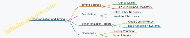
Control Software Robustness and Automation
Lesson: Automation reduces human error and increases repeatability; robust software architectures support fault tolerance and scalability.
Example: A quantum annealing testbed employed FPGA-based real-time controllers integrated with high-level orchestration software, enabling automated calibration and error recovery routines.
Mind Map:
Control Software Mind Map
Data Management and Analytics
Lesson: Efficient data pipelines and analytics tools are necessary to handle large volumes of quantum experiment data and extract meaningful insights.
Example: A photonic quantum testbed integrated machine learning algorithms for real-time qubit state discrimination, significantly speeding up data analysis.
Mind Map:
Data Management Mind Map

Cross-Disciplinary Collaboration and Documentation
Lesson: Large-scale quantum testbeds require collaboration across physics, engineering, software, and management teams, supported by thorough documentation and version control.
Example: A multi-institutional quantum network project used shared repositories and weekly cross-team reviews to ensure alignment and knowledge transfer.
Mind Map:
Collaboration Mind Map
Security and Compliance
Lesson: Protecting sensitive quantum testbed infrastructure and data is vital, especially for projects involving secure communications or proprietary technology.
Example: A quantum key distribution testbed implemented multi-factor authentication and encrypted communication channels between control nodes.
Mind Map:
Security Mind Map

Summary
Large-scale quantum testbed deployments benefit immensely from a systems engineering approach that emphasizes modularity, environmental control, precise synchronization, robust software, efficient data management, collaborative workflows, and security. By learning from past deployments and integrating these best practices, teams can accelerate the development and operational stability of quantum technologies.
For further reading, consider exploring case studies in sections 9.1, 9.2, and 9.4 which provide concrete examples of these lessons in action.
9.4 Example: End-to-End Quantum Communication System Integration
Integrating an end-to-end quantum communication system involves combining quantum hardware, classical control systems, and network infrastructure to enable secure quantum key distribution (QKD) or other quantum communication protocols. This section explores the step-by-step approach, best practices, and illustrative examples to guide systems engineers and testbed managers through the integration process.
Overview of End-to-End Quantum Communication System
An end-to-end quantum communication system typically consists of:
- Quantum Transmitters (e.g., photon sources or entangled photon pairs)
- Quantum Channels (fiber optic cables or free-space links)
- Quantum Receivers (single-photon detectors, measurement devices)
- Classical Control and Post-Processing Units
- Network Management and Security Layers
Mind Map: Components and Integration Layers
Step 1: Defining System Requirements
- Security Goals: Define the level of security required (e.g., unconditional security via QKD).
- Distance and Channel Type: Fiber length or free-space link parameters.
- Key Rate Requirements: Desired key generation rate.
- Integration Constraints: Compatibility with existing classical infrastructure.
Example: For a metropolitan QKD link, a fiber channel of 50 km with a key rate of 1 kbps is targeted.
Step 2: Hardware Selection and Integration
- Photon Source: Choose between weak coherent pulses or entangled photon sources depending on protocol.
- Detectors: Select detectors with low dark count rates and high efficiency.
- Synchronization: Implement precise timing systems to align photon transmission and detection.
Example: Using SNSPDs cooled to 2.5 K integrated with FPGA-based timing electronics for nanosecond synchronization.
Mind Map: Hardware Integration Workflow

Step 3: Classical Control and Post-Processing Integration
- Implement classical communication channels for sifting, error correction, and privacy amplification.
- Develop software modules for real-time key distillation.
- Integrate key management systems for secure storage and distribution.
Example: Deploying a classical Ethernet link parallel to the quantum channel to exchange basis information and perform error correction using LDPC codes.
Step 4: Network and Security Integration
- Integrate quantum keys into existing cryptographic protocols (e.g., AES encryption).
- Implement authentication protocols to prevent man-in-the-middle attacks.
- Ensure compliance with quantum-safe standards.
Example: Using QKD-generated keys to refresh symmetric encryption keys in a VPN tunnel.
Step 5: Testbed Setup and Validation
- Establish environmental controls (temperature, vibration isolation) to maintain hardware performance.
- Implement real-time monitoring dashboards for system health and key rate.
- Perform end-to-end testing including channel loss, error rates, and key generation.
Example: Monitoring photon count rates and quantum bit error rate (QBER) live during a 24-hour test run.
Mind Map: Testbed Monitoring and Validation
Best Practices
- Modular Design: Separate quantum and classical components for easier troubleshooting.
- Redundancy: Use backup detectors and communication channels to improve reliability.
- Automation: Automate calibration and monitoring to reduce human error.
- Documentation: Maintain detailed logs of hardware configurations and software versions.
Summary Example: Metro-Area QKD Deployment
A research team integrated a 50 km fiber-based QKD system using entangled photon pairs. They combined SNSPD detectors with FPGA-based control electronics and classical post-processing software running on a dedicated server. Environmental controls ensured stable operation, while a monitoring dashboard tracked QBER and key rates in real time. The generated keys were used to secure communications between two government offices, demonstrating practical end-to-end quantum communication integration.
This example highlights the importance of cohesive systems engineering, rigorous testing, and seamless integration of quantum and classical components to realize functional quantum communication systems.
9.5 Scaling Quantum Testbeds for Industry Applications
Scaling quantum testbeds from research prototypes to robust platforms suitable for industry applications is a critical step in advancing quantum technologies toward real-world impact. This section explores best practices, challenges, and practical examples to guide systems engineers, testbed managers, and research engineers in this endeavor.
Key Considerations for Scaling Quantum Testbeds
- Modularity: Designing testbeds with modular components allows easy upgrades and integration of new quantum hardware or classical control systems.
- Scalability of Control Systems: Control electronics and software must handle increased qubit counts without compromising latency or fidelity.
- Environmental Stability: Maintaining ultra-low temperatures, vibration isolation, and electromagnetic shielding at scale.
- Data Management: Handling exponentially growing data volumes from large-scale quantum experiments.
- Reliability and Maintenance: Ensuring uptime and ease of troubleshooting in complex setups.
- Interoperability: Supporting diverse quantum technologies and classical interfaces.
Mind Map: Scaling Quantum Testbeds
Best Practices for Scaling
-
Adopt a Layered Architecture: Separate quantum hardware, control electronics, and software into distinct layers with well-defined interfaces. This enables independent upgrades and easier troubleshooting.
-
Implement Distributed Control Systems: Use distributed FPGA or microcontroller units close to qubit modules to reduce latency and improve scalability.
-
Leverage Cloud and Edge Computing: Offload data processing and experiment orchestration to cloud or edge platforms to handle computational demands.
-
Standardize Communication Protocols: Employ industry standards (e.g., OpenQASM, QMI) to facilitate interoperability between components from different vendors.
-
Automate Calibration and Diagnostics: Use AI-driven tools to automate repetitive calibration tasks and detect anomalies early.
-
Design for Maintainability: Modular cabling, accessible components, and comprehensive documentation reduce downtime during maintenance.
Example: Scaling a Superconducting Qubit Testbed from 20 to 100 Qubits
Background: A research lab initially developed a 20-qubit superconducting testbed with custom control electronics and manual calibration.
Scaling Challenges:
- Control electronics bandwidth insufficient for 100 qubits.
- Manual calibration became impractical.
- Increased cryogenic load and thermal management complexity.
Solutions Implemented:
- Introduced modular cryostat inserts allowing incremental qubit addition.
- Upgraded to distributed FPGA-based control units placed near qubit modules.
- Developed automated calibration routines using machine learning to optimize gate fidelities.
- Enhanced vibration isolation with active damping systems.
- Integrated a centralized data pipeline with real-time visualization dashboards.
Outcome: The testbed successfully scaled to 100 qubits with improved system stability and reduced calibration time by 70%, enabling more complex quantum algorithms to be tested.
Mind Map: Example - Scaling Superconducting Qubit Testbed
Example: Industrial Quantum Sensor Testbed Expansion
Scenario: A company developing quantum sensors for precision navigation needed to scale their testbed to support multiple sensor types and environmental conditions.
Approach:
- Designed a flexible testbed platform with plug-and-play sensor modules.
- Integrated environmental chambers to simulate diverse conditions (temperature, pressure, magnetic fields).
- Developed a unified control and data acquisition system supporting heterogeneous sensors.
- Employed containerized software services for easy deployment and updates.
Benefits:
- Accelerated sensor development cycles by enabling parallel testing.
- Improved reproducibility through standardized environmental controls.
- Facilitated collaboration between hardware and software teams via shared interfaces.
Mind Map: Industrial Quantum Sensor Testbed Expansion
Summary
Scaling quantum testbeds for industry applications requires a holistic approach that balances hardware innovation, control system scalability, environmental management, and data infrastructure. By adopting modular designs, automating calibration, and leveraging modern computing paradigms, testbed managers and systems engineers can build robust platforms that accelerate quantum technology commercialization.
The examples provided illustrate practical pathways to overcome common scaling challenges, emphasizing the importance of interdisciplinary collaboration and forward-looking system architectures.
10. Future Directions and Emerging Best Practices
10.1 Advances in Quantum Hardware and Their Impact on Systems Engineering
Quantum hardware is evolving at a rapid pace, bringing transformative changes to systems engineering practices. Understanding these advances is critical for systems engineers, testbed managers, and research engineers to design, integrate, and maintain quantum-ready systems effectively.
Key Advances in Quantum Hardware
-
Qubit Technologies:
- Superconducting Qubits
- Trapped Ion Qubits
- Photonic Qubits
- Topological Qubits
- Spin Qubits
-
Control Electronics:
- Cryogenic Control Systems
- FPGA-Based Real-Time Controllers
- Integrated Quantum-Classical Chips
-
Quantum Interconnects:
- Microwave Links
- Optical Fiber Links
- Quantum Transducers
-
Error Correction Hardware:
- Surface Code Implementations
- Ancilla Qubit Architectures
Mind Map: Advances in Quantum Hardware
Impact on Systems Engineering
-
Modularity and Scalability:
- New qubit types require modular system designs to accommodate different physical constraints.
- Example: Designing a testbed that supports both superconducting and trapped ion qubits by modularizing cryogenic and vacuum components.
-
Environmental Control Complexity:
- Advances like photonic qubits reduce cryogenic requirements but increase optical alignment complexity.
- Example: Integrating vibration isolation and temperature stabilization for hybrid photonic-superconducting testbeds.
-
Control System Integration:
- Cryogenic control electronics enable closer integration but demand new thermal management strategies.
- Example: Using FPGA-based controllers operating at cryogenic temperatures to reduce latency in qubit manipulation.
-
Error Correction Implementation:
- Hardware advances enable real-time error correction, requiring systems to support fast feedback loops.
- Example: Implementing surface code error correction with ancilla qubits and integrating the control software for real-time syndrome decoding.
-
Interconnect and Networking:
- Quantum interconnects facilitate distributed quantum computing, necessitating systems engineering for network synchronization and security.
- Example: Designing a testbed that integrates microwave and optical links for hybrid quantum network experiments.
Mind Map: Impact on Systems Engineering
Example 1: Modular Testbed Supporting Multiple Qubit Technologies
A research lab designed a quantum testbed that supports both superconducting and trapped ion qubits. The systems engineering team created modular cryogenic and vacuum chambers that can be swapped or combined depending on the experiment. Control electronics were designed with flexible interfaces to accommodate different qubit control signals. This modularity allowed rapid prototyping and testing across multiple qubit platforms, accelerating research and reducing costs.
Example 2: FPGA-Based Cryogenic Control Systems
To reduce latency in qubit manipulation, a testbed integrated FPGA controllers operating at cryogenic temperatures near the qubits. This required innovative thermal management to dissipate heat without disturbing the qubit environment. The systems engineering team developed custom heat sinks and employed low-power FPGA designs. This advance improved control fidelity and enabled more complex quantum algorithms to be tested in real-time.
Example 3: Real-Time Error Correction Implementation
A quantum computing startup implemented surface code error correction using ancilla qubits. The systems engineering challenge was to integrate fast syndrome measurement hardware with control software capable of decoding errors and applying corrections within microseconds. The team employed a combination of FPGA-based processing and optimized software pipelines, demonstrating a significant improvement in qubit coherence times and system reliability.
Summary
Advances in quantum hardware are reshaping systems engineering by introducing new requirements for modularity, environmental control, control electronics, error correction, and interconnectivity. Systems engineers must adapt by designing flexible, scalable, and integrated solutions that accommodate emerging quantum technologies. Through modular architectures, innovative control systems, and real-time data processing, quantum-ready systems and testbeds can meet the demands of next-generation quantum applications.
10.2 Best Practice: Preparing Testbeds for Next-Generation Quantum Technologies
As quantum technologies rapidly evolve, preparing testbeds that can accommodate next-generation quantum devices and architectures is critical. This section outlines best practices to future-proof your quantum testbeds, ensuring they remain flexible, scalable, and capable of supporting emerging quantum hardware and software paradigms.
Key Considerations for Next-Generation Quantum Testbeds
- Modularity and Scalability: Design testbeds with modular components that can be upgraded or replaced without overhauling the entire system.
- Advanced Environmental Controls: Incorporate enhanced cryogenic, vibration isolation, and electromagnetic shielding systems to support more sensitive qubit technologies.
- Interoperability: Ensure compatibility with diverse quantum hardware types (e.g., superconducting, trapped ions, photonic) and classical control systems.
- High-Bandwidth and Low-Latency Control: Prepare for increased control complexity and faster feedback loops.
- Data Handling and Analytics: Build infrastructure capable of managing larger data volumes and integrating AI/ML-driven analytics.
Mind Map: Preparing Quantum Testbeds for Next-Generation Technologies
Example 1: Modular Cryogenic Testbed Upgrade for Scalable Qubit Arrays
A research lab initially designed a cryogenic testbed for a 5-qubit superconducting processor. To prepare for next-generation devices with 50+ qubits, they implemented a modular dilution refrigerator insert system. This allowed them to swap out qubit chips and control wiring without warming the entire system, significantly reducing downtime and enabling rapid prototyping.
Best Practices Illustrated:
- Modular hardware design
- Scalable cryogenic infrastructure
- Flexible wiring harnesses for diverse qubit layouts
Example 2: Integrating Photonic Quantum Processors into Existing Testbeds
A testbed originally built for superconducting qubits was adapted to support photonic quantum processors. The team introduced fiber-optic interfaces, upgraded environmental controls to reduce optical noise, and developed new control software modules to handle photonic pulse sequences.
Best Practices Illustrated:
- Interoperability across quantum platforms
- Software modularity for diverse control schemes
- Environmental adaptation for new qubit modalities
Example 3: AI-Driven Calibration and Error Mitigation
To handle the complexity of next-generation quantum devices, a testbed incorporated machine learning algorithms for automated calibration and error mitigation. The system continuously analyzed qubit performance data and adjusted control parameters in real-time, improving fidelity and reducing manual intervention.
Best Practices Illustrated:
- Integration of AI/ML in data analytics
- Automated calibration routines
- Real-time feedback and control
Summary Checklist for Preparing Next-Generation Quantum Testbeds
- Design modular hardware and software components
- Upgrade environmental controls for enhanced sensitivity
- Ensure interoperability with multiple quantum platforms
- Implement high-bandwidth, low-latency control systems
- Build scalable data acquisition and analytics pipelines
- Integrate AI/ML for automation and error correction
- Incorporate security and reliability best practices
By following these best practices, systems engineers and testbed managers can build quantum testbeds that not only meet current needs but also adapt seamlessly to the evolving landscape of quantum technologies.
10.3 Example: Integrating Photonic Quantum Processors into Existing Testbeds
Integrating photonic quantum processors into existing quantum testbeds represents a critical step toward harnessing the unique advantages of photonic quantum computing—such as room-temperature operation, high-speed data transmission, and ease of integration with fiber-optic networks. This section explores the practical considerations, best practices, and illustrative examples for achieving seamless integration.
Understanding Photonic Quantum Processors
Photonic quantum processors use photons as qubits, manipulated through linear optical elements, nonlinear interactions, and measurement-based protocols. Unlike superconducting or ion-trap qubits, photonic qubits are inherently compatible with optical fiber networks, enabling distributed quantum computing and communication.
Key Integration Challenges
- Interface Compatibility: Bridging electronic control systems with optical components.
- Environmental Requirements: Managing temperature stability and vibration isolation for optical setups.
- Synchronization: Aligning timing between photonic qubit generation, manipulation, and measurement.
- Data Acquisition: Capturing high-speed photon detection events with low latency.
Best Practices for Integration
- Adopt modular interface layers to decouple photonic components from classical control electronics.
- Utilize FPGA-based timing controllers for precise synchronization.
- Implement fiber-optic connectors and switches standardized for testbed compatibility.
- Design flexible software APIs that abstract photonic device control.
Mind Map: Photonic Quantum Processor Integration Workflow
Example: Integrating a Silicon Photonic Processor into a Superconducting Qubit Testbed
Scenario: A research team aims to integrate a silicon photonic quantum processor module into an existing cryogenic testbed primarily designed for superconducting qubits.
Steps Taken:
-
Interface Adaptation: Developed a custom optical fiber feedthrough compatible with the cryostat to route photons into the photonic chip inside the cryogenic environment.
-
Control Electronics: Employed FPGA-based timing controllers synchronized with the superconducting qubit control system to coordinate photon generation and qubit operations.
-
Environmental Management: Installed vibration damping mounts and temperature sensors to monitor and stabilize the photonic chip environment.
-
Software Integration: Extended the testbed’s control software with new modules to handle photonic device commands and photon detection event logging.
-
Validation: Conducted joint quantum gate operations involving both superconducting and photonic qubits, verifying coherence and entanglement fidelity.
Mind Map: Example Integration Architecture
Additional Example: Fiber-Optic Network Integration for Distributed Photonic Quantum Processors
In a distributed quantum computing testbed, multiple photonic quantum processors are connected via fiber-optic links enabling entanglement distribution and quantum communication.
Key Integration Elements:
- Standardized fiber connectors and switches for flexible routing.
- Quantum-compatible wavelength division multiplexing (WDM) to maximize channel capacity.
- Real-time synchronization protocols to coordinate photon emission and detection across nodes.
- Centralized control software managing distributed resources and data aggregation.
Summary
Integrating photonic quantum processors into existing testbeds demands a holistic approach encompassing hardware adaptation, environmental control, precise synchronization, and software interoperability. By following modular design principles and leveraging advanced control electronics, systems engineers can create versatile quantum testbeds that harness the strengths of photonic technologies alongside other quantum platforms.
10.4 Embracing Automation and AI in Quantum Systems Testing
As quantum technologies advance rapidly, the complexity and scale of quantum systems testing increase correspondingly. Automation and Artificial Intelligence (AI) have become indispensable tools to enhance efficiency, accuracy, and scalability in quantum testbeds. This section explores how automation and AI can be integrated into quantum systems testing, illustrating best practices with practical examples and conceptual mind maps.
Why Automation and AI in Quantum Testing?
- Complexity Management: Quantum systems involve numerous parameters (e.g., qubit coherence times, gate fidelities) that require precise tuning and monitoring.
- Speed and Scalability: Manual testing is time-consuming; automation accelerates repetitive tasks and enables large-scale experiments.
- Data-Driven Insights: AI algorithms can analyze complex datasets to identify patterns and optimize system performance.
Key Areas Where Automation and AI Impact Quantum Testing
Best Practices for Implementing Automation and AI
-
Modular Automation Frameworks:
- Use modular software architectures (e.g., Python-based frameworks) to automate pulse generation, experiment scheduling, and data collection.
- Example: Employing QCoDeS, an open-source Python-based data acquisition framework, to automate quantum experiments.
-
Integration of Machine Learning Models:
- Apply supervised and reinforcement learning to optimize qubit calibration and gate operations.
- Example: Using Bayesian optimization to find optimal control parameters that maximize qubit coherence.
-
Real-Time Feedback Loops:
- Implement closed-loop control where AI algorithms analyze measurement outcomes and adjust control parameters on-the-fly.
- Example: Adaptive error correction protocols that adjust based on detected error syndromes.
-
Data Management and Visualization:
- Automate data labeling, storage, and visualization to facilitate rapid decision-making.
- Example: Dashboards that display live qubit performance metrics and alert operators to anomalies.
-
Cross-Disciplinary Collaboration:
- Combine expertise from quantum physics, software engineering, and AI to build robust automated testbeds.
Example 1: Automated Qubit Calibration Using AI
A superconducting qubit testbed integrates an AI-driven calibration system:
-
Process:
- The system performs initial rough calibration using predefined pulse sequences.
- A Bayesian optimization algorithm iteratively adjusts pulse parameters to maximize gate fidelity.
- Calibration results feed into a machine learning model predicting optimal parameters for similar qubits.
-
Benefits:
- Calibration time reduced by 50% compared to manual tuning.
- Improved gate fidelities due to fine-grained parameter optimization.
Example 2: Automated Error Detection and Correction Testing
In an ion-trap quantum testbed:
-
Automation:
- Automated scripts run sequences of error correction codes.
- AI algorithms analyze syndrome measurement data to detect error patterns.
-
AI Role:
- Reinforcement learning agents adapt error correction strategies based on historical performance.
-
Outcome:
- Improved error correction efficiency.
- Reduced human intervention in iterative testing cycles.
Challenges and Considerations
- Data Quality: AI models require high-quality, labeled data; noisy quantum measurements can complicate training.
- Computational Resources: Real-time AI processing demands efficient hardware integration.
- Interpretability: Understanding AI decisions is critical for trust and debugging.
- Scalability: Automation frameworks must scale with increasing qubit counts and system complexity.
Summary
Embracing automation and AI in quantum systems testing is a transformative best practice that accelerates development cycles, enhances precision, and enables scalable quantum technologies. By combining modular automation frameworks with intelligent algorithms, quantum testbeds become more adaptive, efficient, and capable of meeting the demands of next-generation quantum engineering.
10.5 Roadmap for Quantum-Ready Systems Engineering and Testbed Evolution
As quantum technologies rapidly evolve, systems engineers and testbed managers must adopt a forward-looking roadmap to ensure their infrastructures remain quantum-ready and scalable. This section outlines a comprehensive roadmap emphasizing key milestones, best practices, and practical examples to guide the evolution of quantum systems engineering and testbeds.
Key Phases in the Roadmap
Phase 1: Foundation & Capability Building
- Develop Quantum Literacy: Train systems engineers and testbed managers on quantum fundamentals and emerging hardware.
- Establish Modular Testbeds: Build flexible testbeds that support multiple quantum platforms (e.g., superconducting, trapped ions).
- Integrate Classical-Quantum Interfaces: Design robust interfaces for seamless communication between classical control electronics and quantum processors.
Example: A university quantum lab upgraded its existing classical control system by incorporating modular FPGA boards tailored for superconducting qubit control. This enabled rapid prototyping and easy swapping of control modules without disrupting the entire setup.
Phase 2: Advanced Integration & Automation
- Implement AI-driven Control Systems: Use machine learning algorithms to optimize qubit calibration and error mitigation.
- Enhance Real-Time Data Analytics: Deploy streaming analytics to monitor qubit performance and environmental conditions.
- Scale Testbeds for Multi-Qubit Systems: Expand testbed capacity to handle tens or hundreds of qubits while maintaining low noise and latency.
Example: A national research institute integrated a reinforcement learning algorithm into their ion trap testbed control software, which dynamically adjusted laser parameters to improve qubit coherence times by 15%.
Phase 3: Industry-Grade Deployment & Standardization
- Adopt Security & Compliance Standards: Implement quantum-safe communication protocols and comply with emerging quantum engineering standards.
- Foster Cross-Industry Collaborations: Share testbed resources and best practices across academia, government, and industry.
- Deploy Robust Fault-Tolerant Systems: Incorporate error correction codes and redundancy in both hardware and software layers.
Example: A consortium of companies and universities established a shared quantum testbed network with standardized APIs and security protocols, enabling collaborative development of quantum algorithms and hardware validation.
Phase 4: Next-Gen Quantum Ecosystems
- Integrate Photonic and Topological Qubits: Prepare testbeds to support emerging qubit technologies with unique control and environmental requirements.
- Automate End-to-End Quantum Workflows: Develop fully automated pipelines from system calibration to experiment execution and data analysis.
- Enable Hybrid Quantum-Classical Cyber-Physical Systems: Seamlessly embed quantum processors into larger cyber-physical infrastructures for real-world applications.
Example: A startup developed a testbed integrating photonic quantum processors with classical edge computing devices, enabling real-time quantum-enhanced sensing in industrial environments.
Comprehensive Mind Map: Quantum-Ready Systems Engineering Roadmap
Summary
This roadmap serves as a strategic guide for systems engineers, testbed managers, and research engineers to evolve their quantum infrastructures in alignment with technological advances and industry needs. By following these phases and adopting the highlighted best practices and examples, organizations can build resilient, scalable, and future-proof quantum-ready systems and testbeds.